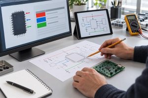
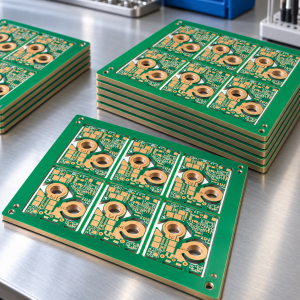
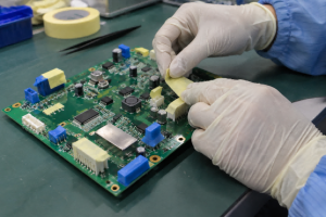
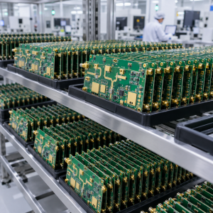
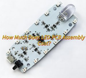
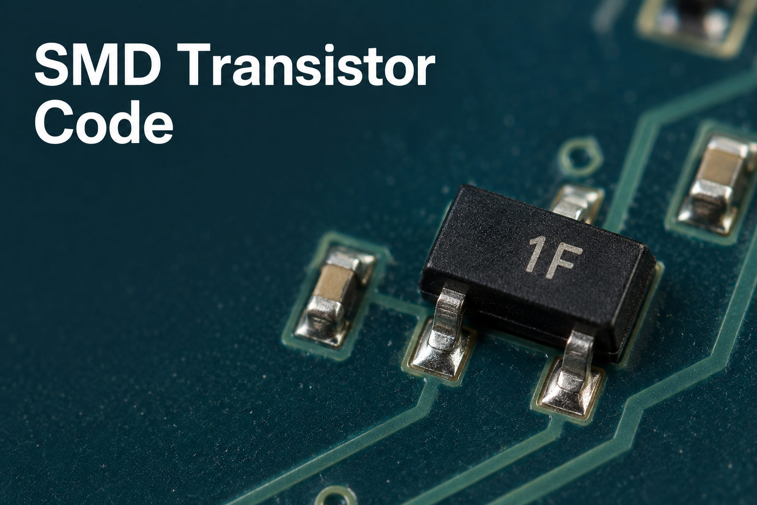
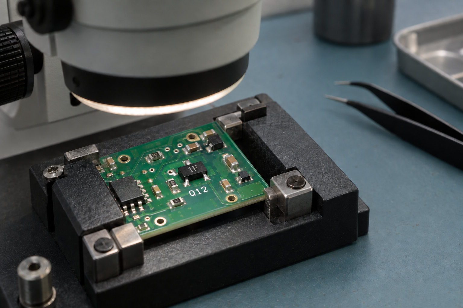
A QR code on PCB links a circuit board to production, test, repair, or warranty records. It may open a technical document or provide a unique serial number for each unit.
The finished mark must remain readable after fabrication, reflow, cleaning, coating, and assembly. Its size, contrast, placement, and marking method all matter.
Static codes often suit PCB silkscreen. Unit-level serial numbers normally require laser marking, inkjet coding, or variable-data labels. Data Matrix may be better when board space is limited.
What Is a QR Code on PCB?
A QR code on PCB is a machine-readable 2D symbol placed on a bare circuit board, assembled PCBA, production panel, or label. It can contain text, URLs, serial numbers, or a reference to an external database.
PCB QR codes generally fall into 2 categories:
Static QR code: The same information appears on every board, such as a product number, website, manual, or assembly document.
Serialized QR code: Each board receives a unique code linked to its production lot, test record, firmware version, repair history, or warranty information.
A static code can be included in the Gerber silkscreen layer. A serialized code changes from board to board, so it needs a variable-data process such as laser marking, inkjet printing, or automated label application.
A PCB-level code identifies the board, panel, or assembled product, while codes on IC packages identify individual components.
Why Are QR Codes Used on Circuit Boards?
QR codes improve identification and traceability while reducing manual data entry.
Typical applications include:
PCB part number and revision identification
Production lot and manufacturing date tracking
Panel and unit position recording
AOI, X-ray, ICT, and functional test linking
Firmware programming records
Repair and warranty history
Access to drawings, manuals, and service instructions
Anti-counterfeit verification
A bare PCB code may identify the fabrication lot, material batch, and revision. A PCBA code can also link component lots, SMT inspection results and functional tests, and firmware.
In high-volume production, each workstation can scan the code and update the same MES record. If an issue appears later, affected boards can be isolated quickly.
The code should therefore match the record structure used by the factory. A serial number that cannot be connected to material, process, and test data provides identification, but not complete traceability. Before production, confirm which fields will be stored, who can update them, and how long the records must remain available.
What Information Can a PCB QR Code Store?
A QR code can hold substantial data, but more characters create a denser symbol. Dense codes need smaller modules or more board area, both of which reduce manufacturing tolerance.
For PCB applications, it is usually better to encode a short identifier such as:
Part number
PCB revision
Serial number
Manufacturing lot
Production date
Panel and unit position
Test record ID
Firmware reference
Short database URL
For example, PCB-260722-P18-U04 could identify a production date, panel, and unit position. Detailed material, inspection, test, firmware, and repair data can remain in a linked database.
Sensitive data should not be written directly into an open QR code. Use the code as a record key and protect the linked system with access control.
How Can You Add a QR Code to a PCB?
Select the marking method according to data variability, code size, durability, board material, and production stage.
Marking method
Best suited for
Main advantages
Main limitations
PCB silkscreen
Static codes
Low additional cost and included in standard PCB artwork
Limited resolution and no unit-level variation
Laser marking
Unique serial numbers
Permanent, precise, and easy to automate
Additional process cost and parameter setup
High-temperature label
Variable data and readable text
Strong contrast and flexible format
Label and adhesive must survive assembly
Copper or solder mask pattern
Large static codes
Integrated into the PCB structure
Uses more board area and may have weak contrast
Inkjet marking
Automated variable coding
Fast and contactless
Ink durability must be validated
PCB Silkscreen
Silkscreen suits projects where the same code appears on every PCB. The symbol is added to the legend layer and printed during standard fabrication.
Use vector artwork or generate the code directly in PCB design software. Screenshots and compressed bitmaps may produce uneven modules after Gerber conversion. Fine ink areas can also spread, merge, or become incomplete.
Laser Marking
Laser marking is usually preferred for unit-level serialization. The software generates a different code for each PCB without changing the Gerber files.
It can support automatic numbering, camera alignment, scan verification, duplicate detection, and database registration. Laser parameters must match the solder mask and laminate. Excessive energy may expose copper, while insufficient energy produces weak contrast.
High-Temperature Labels
Labels can carry both a QR code and human-readable text. They are useful when information changes late in production or strong contrast is required.
The material and adhesive must survive:
Lead-free reflow
Flux and cleaning chemicals
Conformal coating
Operating temperature and humidity
General-purpose labels are not suitable for electronics assembly.
Copper or Solder Mask Patterns
A static code can also be formed with exposed copper or solder mask openings. This creates a permanent mark without ink, but it uses more board space.
Fine copper islands and narrow solder mask webs may exceed standard fabrication capability, so this method needs DFM review.
How Does Laser QR Code Marking Work on PCB?
A laser QR code on PCB creates a permanent code on the PCB surface after solder mask processing. It is suitable for variable data because every board can receive a unique serial number.
A typical process includes:
Define the serial-number format and starting value.
Position the PCB or panel using fixtures or camera alignment.
Set laser power, speed, focus, and pulse parameters.
Generate and mark the QR code.
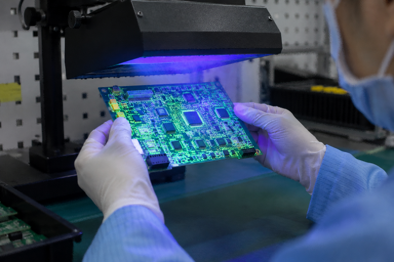
Scan and verify the finished code.
Save the result to the production database.
The laser creates contrast by removing or changing a thin surface layer without damaging the PCB structure.
The marking stage should be defined in advance. Marking before assembly provides clear surface access, but the code may later be covered by components, heat sinks, shields, connectors, or an enclosure. Marking after assembly avoids some of these risks but requires a safe area away from sensitive parts.
For quotation, specify whether the code is required on the production panel, each bare PCB, each assembled PCBA, or the final enclosure. Panel-level marking supports process tracking, but it disappears when the rail is removed.
What Size Should a QR Code on PCB Be?
There is no universal minimum size. The correct dimensions depend on:
Encoded data length
QR version
Error-correction level
Module size
Marking process
Surface contrast
Scanner type
Reading distance
A QR code is built from square modules:
Code width = total modules × module size
A Version 1 QR code contains a 21 × 21 module data area. After adding a 4-module quiet zone on each side, the total area becomes 29 × 29 modules.
With a 0.30 mm module:
29 × 0.30 mm = 8.70 mm
This is a geometric size, not a guaranteed manufacturing limit. Silkscreen ink spread, solder mask texture, reflection, and registration tolerance may require a larger code.
Do not approve the design from a screen image alone. A useful prototype check should include several finished boards, the planned scanner, normal production lighting, and the expected reading distance. The code should also be tested after any cleaning, coating, or assembly step that could change contrast or block access.
To improve scan reliability:
Keep the encoded string short.
Use the largest practical module size.
Preserve the complete quiet zone.
Avoid uneven scaling.
Use vector artwork.
Test with the intended scanner.
Approve a fabricated sample.
Laser marking can normally support smaller modules than silkscreen. When board space is limited, shorten the identifier or consider Data Matrix. Scanner capability should be confirmed early because an industrial camera may read a smaller code than a smartphone.
Where Should You Place a QR Code on a PCB?
Place the code in a flat, open area that remains visible when scanned.
A suitable location should:
Stay clear of pads, vias, test points, and exposed copper
Include enough space for the full quiet zone
Remain away from routed edges, V-scores, slots, and mounting holes
Avoid components, shields, connectors, heat sinks, and cables
Remain visible after enclosure assembly
Use a consistent orientation for automated scanning
Avoid highly reflective surfaces
Remain readable after coating and cleaning
The top side is often easier to scan; the bottom may offer more space but become inaccessible after installation.
A code on the panel rail can track fabrication and SMT, but it disappears after depanelization. Permanent traceability therefore requires a code on each PCB.
Placement should be reviewed before layout release. Late additions often cause insufficient quiet zone, fixture interference, component coverage, or poor scanner access.
QR Code vs Data Matrix: Which Is Better for PCB Traceability?
The main decision is whether smartphone readability or compact size matters more.
Selection factor
QR Code
Data Matrix
Data density
Good
Higher for compact industrial data
Smartphone compatibility
Widely supported
Less consistent
Industrial scanner support
Excellent
Excellent
Required PCB area
Usually larger
Usually smaller
Typical use
Manuals, warranty, websites, field service
Factory serialization and MES tracking
Suitability for small PCBs
Moderate
Strong
Human recognition
High
Lower
Laser marking
Suitable
Very suitable
Use QR Code for smartphone access and Data Matrix when space is limited and industrial cameras handle the reading. Confirm scanner compatibility before finalizing the symbol.
Why Does a QR Code on PCB Fail to Scan?
Most failures come from the physical marking process rather than the QR logic.
Modules Are Too Small
Fine silkscreen modules may merge, spread, or disappear.
Fix: Increase module size, shorten the encoded value, or use laser marking.
The Quiet Zone Is Blocked
Nearby text, copper, vias, solder mask openings, or board edges can interfere with detection.
Fix: Treat the quiet zone as a layout keep-out area.
Contrast Is Too Low
Glossy solder mask, reflective metal, or weak laser marks reduce readability.
Fix: Evaluate the finished board under real lighting.
The Artwork Was Distorted
Uneven resizing or bitmap conversion changes module proportions.
Fix: Keep a 1:1 aspect ratio and use vector artwork.
Too Much Data Is Encoded
Long URLs and detailed text create dense codes.
Fix: Encode a short ID or database reference.
Reflection or Contamination Interferes
ENIG, coating, flux residue, or dust can blur the code.
Fix: Adjust placement or lighting and verify the code after the final surface process.
Components Cover the Code
A code may scan on the bare PCB but become inaccessible after assembly.
Fix: Review the final 3D assembly and enclosure.
A PCB QR code scanner should be validated for the planned lighting and reading distance. For mass production, define the scanner model, scan distance, lighting, inspection stage, and whether verification is sampled or performed on every unit.
How Should You Specify PCB QR Code Requirements to a Manufacturer?
Clear specifications allow the manufacturer to select the right process and quote accurately.
Provide:
QR Code or Data Matrix
Static or variable data
Bare PCB or assembled PCBA
Silkscreen, laser, inkjet, or label
Encoded content and data format
Serial-number sequence and starting value
Code dimensions
Marking side and coordinates
Required orientation
Solder mask color
Panel-level or unit-level marking
Human-readable text
Scanner type
Verification requirement
Reflow, cleaning, coating, and temperature conditions
MES or database integration requirements
A practical specification may look like this:
Format: BT26-XXXXXX
Starting number: BT26-000001
Quantity: 2,000
Process: laser marking
Code size: 8 × 8 mm
Location: bottom side
Human-readable text: serial number below the code
Inspection: scan every unit after marking
For prototypes, scan marked samples after assembly, cleaning, and coating.
EBest Circuit can review code location, contrast, serialization, panel arrangement, and marking method during DFM and quotation. Submit the QR specification with Gerber files, BOM, assembly drawings, and test requirements.
FAQ
1. What is the minimum size for a QR code on PCB?
There is no fixed minimum size. It depends on the marking method, module size, data length, surface contrast, and scanner. A fabricated sample should be tested before mass production.
2. Is laser marking better than silkscreen for PCB QR codes?
Laser marking is better for unique serial numbers, smaller symbols, and permanent traceability. Silkscreen is more economical for larger static codes.
3. Can a QR code survive PCB reflow soldering and cleaning?
Silkscreen and properly controlled laser marks normally survive standard assembly. Labels must be rated for reflow, flux, cleaning chemicals, and operating temperature.
4. Can every PCB have a unique QR code?
Yes. Laser marking, inkjet printing, and variable-data labels can generate a different code for each board.
5. Can a smartphone scan a QR code on a circuit board?
Yes. A QR code on circuit board surfaces can be scanned when the code has sufficient size, contrast, quiet zone, and visibility. Very small industrial codes may require a dedicated scanner.
6. Should I use QR Code or Data Matrix on a small PCB?
Data Matrix is usually more space-efficient. QR Code is preferable when smartphone compatibility is important.
7. What file format should be used for a PCB QR code?
Use vector artwork or generate the code directly in PCB design software. Avoid screenshots and compressed images.
8. Why does a QR code scan on screen but fail on the finished PCB?
Common causes include small modules, silkscreen ink spread, low contrast, reflection, blocked quiet zones, coating, or distorted artwork.
Need QR Code Support for Your PCB Project?
Before requesting a quotation, define the code format, size, marking stage, serial-number rule, scanner, and verification method. EBest Circuit can review QR code placement, laser marking, panel serialization, and PCBA traceability requirements during DFM.
What Is Solder Wicking in PCB Assembly? Solder wicking in PCB assembly is the unwanted movement of molten solder away from the intended solder joint. It usually happens because of capillary action, heat imbalance, open vias, exposed copper, improper solder paste volume, or unsuitable reflow conditions. When solder leaves the pad, the result may be a weak joint, dry joint, insufficient solder, open connection, or long-term reliability risk.
For EBest Circuit (Best Technology), solder wicking is not only a soldering term. It is a real PCBA quality issue that may appear in PCB SMT assembly, through-hole soldering, BGA assembly, via-in-pad structures, connector areas, and rework. If your PCB assembly project has solder joint, BGA, via-in-pad, SMT, stencil, reflow, or inspection concerns, please feel free to send your Gerber files, BOM, assembly drawing, PCB stackup, or soldering notes to sales@bestpcbs.com. Our engineering team can review the manufacturing path before production starts.
What Is Solder Wicking in PCB Assembly?
What is solder wicking? Solder wicking means molten solder is pulled away from the place where it should form a joint.
In PCB assembly, solder should stay between the component terminal and the PCB pad. If it flows into a via, up a component lead, along exposed copper, or into stranded wire, the solder volume left at the joint may become insufficient.
Common results include:
weak solder joints
dry or dull solder joints
insufficient solder on pads
open circuits
poor mechanical strength
unstable electrical contact
difficult inspection results
higher rework risk
Solder wicking is especially important in high-density PCBA projects because small pads, fine-pitch components, via-in-pad designs, BGA areas, connectors, and compact layouts leave less process margin.
Solder Wick vs Solder Wicking
Solder wick and solder wicking sound similar, but they are not the same thing.
Term
Meaning
Solder wick
A desoldering braid used to remove solder
Solder wicking
A solder flow defect or process risk
Desoldering wick
Another name for solder wick
Wicking solder
Solder being pulled away by capillary action
A solder wick is usually a braided copper strip with flux. It is used during rework or repair to remove extra solder from pads, bridges, or component leads.
Solder wicking, however, is usually unwanted. It means solder has moved away from the joint during soldering, reflow, wave soldering, hand soldering, or repair.
For PCB assembly projects, this distinction matters because the solution is different. Solder wick is a rework tool used to remove solder, while solder wicking is a process risk that should be prevented through PCB layout review, via control, solder mask design, stencil planning, and assembly inspection.
What Is Solder Wick Used For?
Solder wick is used to remove solder from a PCB during repair, prototype adjustment, or rework.
It is often used for:
removing solder bridges
cleaning pads before replacing components
correcting excess solder
removing solder from through-hole pads
preparing pads for reassembly
repairing prototype boards
cleaning fine-pitch IC pads carefully
The basic working principle is simple. The heated solder melts, and the braided copper wick pulls the solder into itself through capillary action. Flux helps improve wetting and solder flow.
However, solder wick should be used carefully. Too much heat, too much pressure, or long contact time can damage pads, solder mask, copper traces, or nearby components. If rework is needed on a prototype or assembled PCB, the process should follow a controlled method for how to use solder wick and should be inspected after repair.
What Causes Solder Wicking on PCB Assemblies?
Solder wicking usually has more than one cause. It may come from PCB layout details, fabrication choices, assembly process settings, or repair conditions.
Cause
What Happens
Open via near pad
Solder flows into the via
Via-in-pad not filled
Solder drains away from the component pad
Exposed copper path
Solder spreads beyond the joint
No solder mask dam
Solder moves toward nearby copper
Too much heat
Solder becomes too fluid
Long heating time
Solder keeps flowing before solidifying
Wrong paste volume
Joint receives too little or too much solder
Poor pad design
Solder balance becomes unstable
Wire strands
Solder climbs into the wire
Rework error
Excessive heat pulls solder away
The core issue is usually capillary action. Molten solder is pulled into narrow spaces such as vias, gaps, copper braid, wire strands, or plated holes. If the PCB design or assembly process gives solder an easier path than the intended joint, wicking becomes more likely.
Solder Wicking in Via-in-Pad and BGA Assembly
Solder wicking is a serious concern in via-in-pad and BGA assembly.
In a BGA area, vias may be placed inside or near pads to support dense routing. If those vias are open, solder can flow into the via during reflow. This may leave too little solder between the BGA ball and the pad.
Possible problems include:
weak BGA joints
insufficient solder volume
hidden opens
poor coplanarity after reflow
unreliable thermal cycling performance
difficult X-Ray judgment
For via-in-pad designs, common manufacturing controls include resin-filled vias, plated-over vias, planarization, solder mask control, and proper pad definition. These points should be confirmed before PCB fabrication, not after SMT assembly.
For BGA-related projects, EBest Circuit can review whether the PCB fabrication process, via treatment, surface finish, solder mask opening, and assembly notes match the customer’s production requirements.
You may also refer to our guide on BGA soldering when reviewing BGA assembly risks.
Solder Wicking in Through-Hole Components and Wires
Solder wicking can also happen in through-hole components and wires.
For through-hole components, solder may climb up the lead instead of staying around the plated through hole and pad. This can happen when the lead, hole size, heating time, flux activity, and solder volume are not balanced.
For stranded wires, solder can travel up the wire strands. A small amount of solder flow may be acceptable in some cases, but too much wicking can make the wire stiff. This may create mechanical stress near the solder joint, especially when the wire bends during use.
Areas that need attention include:
connectors
terminal blocks
wire-to-board joints
power input areas
hand-soldered components
reworked pads
cable assemblies
high-vibration applications
For PCBA projects with wires or through-hole parts, the assembly notes should clearly define soldering requirements, acceptable solder height, cleaning needs, inspection standard, and packing method.
How to Prevent Solder Wicking During SMT Assembly
Solder wicking prevention should start before production.
Useful checks include:
keep vias away from pads when possible
use filled and capped vias for via-in-pad
maintain enough solder mask dam between pads and vias
confirm pad size and solder mask opening
review stencil aperture design
control solder paste volume
check reflow profile
avoid excessive heating during rework
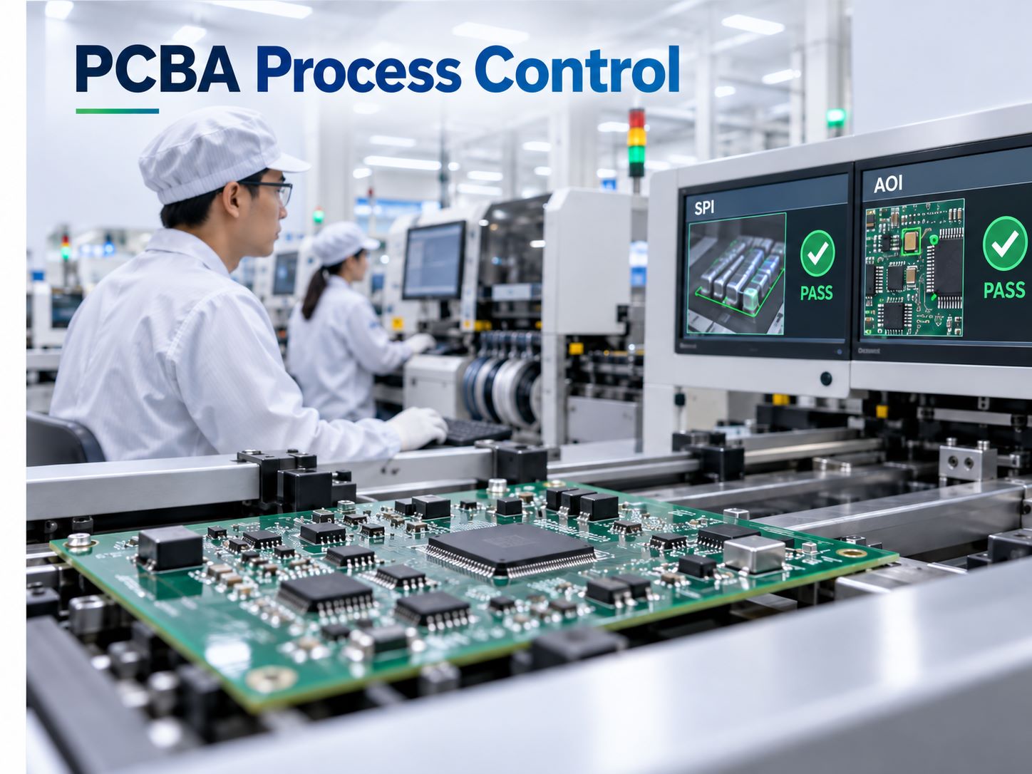
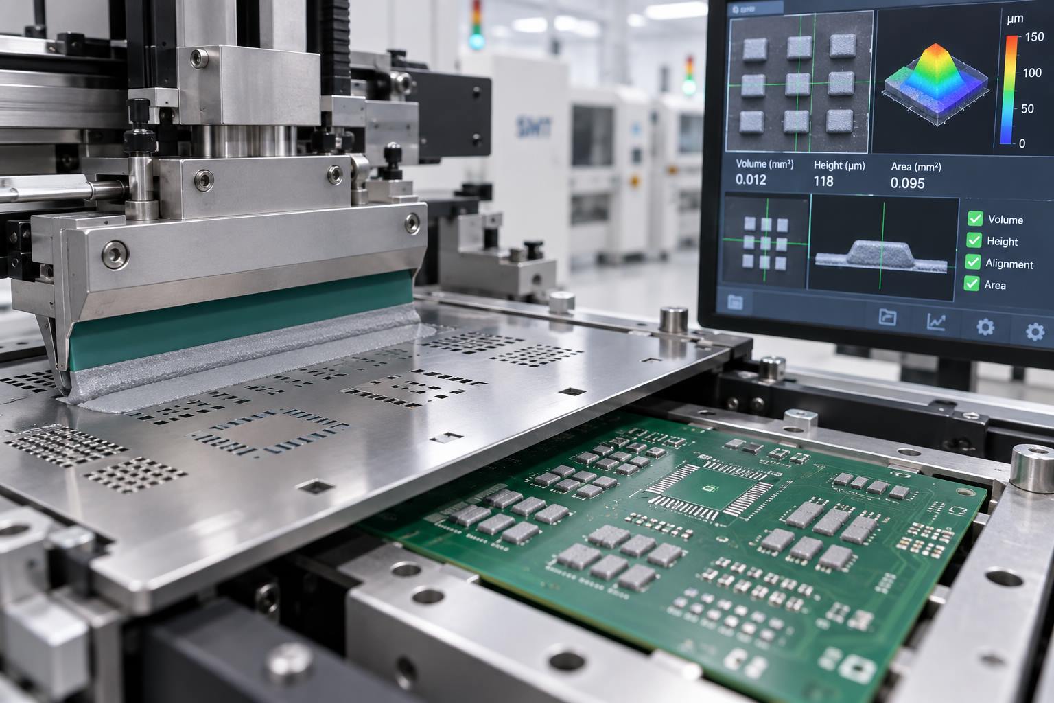
inspect solder paste printing with SPI
inspect finished solder joints with AOI or X-Ray when needed
For SMT assembly, the solder paste process is especially important. If paste volume is too low, the joint may be weak. If paste volume is too high, solder may bridge or flow into unwanted areas. The correct stencil design depends on pad size, component type, pitch, paste type, board finish, and assembly risk.
Reflow temperature also matters. A profile that is too aggressive may increase solder flow problems. A profile that is too weak may cause poor wetting. The right profile should match the solder paste, component thermal mass, PCB thickness, copper distribution, and assembly complexity.
You may also find our guide on solder temperature for PCB useful when reviewing soldering process conditions.
How to Inspect and Repair Solder Wicking Defects
Solder wicking defects should be checked at the right process stage.
Inspection methods may include:
visual inspection
SPI after solder paste printing
AOI after reflow
X-Ray for BGA, QFN, and hidden joints
electrical testing
functional testing
microscope inspection for rework areas
A solder wicking defect may not always be obvious from the surface. In BGA or via-in-pad assembly, the problem may be hidden under the component. That is why X-Ray inspection is important for selected high-risk packages.
Repair depends on the defect type. Some joints can be corrected by controlled rework. Some BGA or via-in-pad issues may require component removal and reballing or replacement. If the root cause is open via-in-pad design or insufficient via filling, repair alone may not solve the problem for future batches.
A good repair process should answer three questions:
Is the solder joint electrically reliable?
Is the solder joint mechanically reliable?
Has the root cause been corrected before the next build?
EBest Circuit PCBA Quality Control for Solder Wicking Risks
EBest Circuit controls solder wicking risks as part of the full PCB and PCBA manufacturing process.
Our support includes:
DFM review before production
PCB fabrication process review
via-in-pad and resin-filled via review
solder mask opening check
BOM and assembly file review
SMT process planning
solder paste printing control
SPI, AOI, and X-Ray support when required
through-hole and hand soldering process control
rework and inspection support
prototype and small-batch production
This is important because solder wicking is not only an operator issue. It may come from the PCB structure, via design, pad design, solder mask, stencil, paste volume, reflow profile, component type, or rework method.
EBest Circuit provides one-stop PCB fabrication, component sourcing, PCBA assembly, testing coordination, and engineering review. For projects with BGA, fine-pitch ICs, via-in-pad, connectors, wire soldering, or high-reliability requirements, this integrated workflow helps keep manufacturing details visible from file review to final delivery.
FAQs about Solder Wicking and Solder Wick
1. What is solder wicking? Solder wicking is the unwanted movement of molten solder away from the intended solder joint. In PCB assembly, it may cause insufficient solder, weak joints, dry joints, or open connections.
2. Is solder wick the same as solder wicking? No. Solder wick is a desoldering braid used to remove solder. Solder wicking is a solder flow problem or defect where solder is pulled away from the joint.
3. What is solder wick used for? Solder wick is used for removing solder bridges, cleaning pads, repairing prototype boards, and preparing pads for component replacement during rework.
4. How do you prevent solder wicking in PCB assembly? Prevention methods include proper via placement, filled via-in-pad, solder mask dams, correct stencil aperture, controlled solder paste volume, suitable reflow profile, and inspection after SMT.
5. Why is solder wicking a problem in BGA assembly? In BGA assembly, solder wicking may pull solder into open vias or away from pads. This can create weak or hidden solder joints that may require X-Ray inspection.
In summary, if your PCB or PCBA project involves BGA assembly, via-in-pad, fine-pitch SMT, through-hole soldering, connector soldering, rework, or solder joint quality concerns, please feel free to contact sales@bestpcbs.com. EBest Circuit’s engineering team can help review your files and manufacturing notes before production, so soldering risks are addressed earlier instead of discovered after assembly.
If you are comparing PCB manufacturers for a Singapore project, build the shortlist around PCB/PCBA scope, certificates, DFM response, service type, quote clarity and delivery planning. A supplier name is useful only after the company explains how it will quote, manufacture, assemble, inspect and ship your actual project.
EBest Circuit directly serves Singapore buyers that need PCB fabrication, PCBA service, BOM/CPL review, DFM feedback, component sourcing, testing support and production planning in one RFQ path.
Before choosing a PCB supplier for Singapore projects, check whether the quote covers the whole build path.
Singapore buyers often need fast engineering communication, stable PCBA support and clear delivery planning. The risk is choosing a supplier that prices the bare PCB first but leaves BOM/CPL review, components, assembly, testing and shipping unclear.
The first quote covers bare PCBs only, while assembly, component sourcing, stencil, inspection, testing and freight are added later.
The supplier says the board is manufacturable, but does not confirm stackup, material, finish, copper, hole limits, panelization or assembly clearance.
BOM/CPL problems, unavailable components, package mismatches or polarity questions are found only when assembly is already waiting.
The prototype can be built once, but nobody explains what must change before low-volume or repeat production.
The lead time is given as one number, without separating PCB fabrication, component sourcing, assembly, testing, packing and shipping.
EBest Circuit helps Singapore buyers turn supplier comparison into a checked PCB and PCBA plan before quote approval.
We review Gerber or ODB++ files, stackup, material notes, surface finish, quantity, testing needs and delivery goals before quote approval.
We connect bare-board fabrication with PCBA, BOM/CPL review, component sourcing and assembly planning.
We help catch DFM questions early, so the buyer can fix design, panel, soldering, hole, material or assembly issues before production starts.
We review sourcing risk before assembly, especially where substitutes, MOQ, package availability or long-lead components can change schedule.
We help plan prototype, low-volume and production builds with the next stage in mind, instead of treating every order as a one-time sample.
Top 12 PCB Manufacturer Options for Singapore RFQ Shortlists
Use this list to build an RFQ shortlist, then compare each supplier with the same files and the same scope questions. Exact capability, MOQ, inspection, testing and delivery should still be confirmed directly with each supplier.
1. EBest Circuit
Main Products / PCB or PCBA Type: Rigid PCB, flex PCB, HDI PCB, PCBA, DFM and BOM/CPL review
Certifications: IATF 16949, ISO 9001, ISO 13485, UL, RoHS, REACH
Service Type: Prototype, low volume, production, PCBA
Location / Service Region: Directly serves Singapore buyers
2. MPN Tech
Main Products / PCB or PCBA Type: PCB design, fabrication, assembly, component sourcing and R&D prototyping
Certifications: ISO 9001, ISO 14001, ISO 13485 listed on PCB Directory
Service Type: Prototype, no-minimum assembly, production support
Location / Service Region: Jurong East, Singapore
3. Wizlogix
Main Products / PCB or PCBA Type: PCB design, prototype, production support and technical PCB services
Certifications: AS9100D, ISO 9001:2015
Service Type: PCB design, manufacturing management, assembly support
Location / Service Region: Singapore
4. Statron Technology
Main Products / PCB or PCBA Type: Turnkey PCB assembly, rework, testing and high-mix PCBA
Certifications: ISO 9001:2015; IPC Class-3 specialists listed on PCB Directory
Service Type: Prototype, low-to-mid volume PCBA, testing
Location / Service Region: Singapore
5. Promax PCB
Main Products / PCB or PCBA Type: PCB fabrication and printed circuit board manufacturing service
Certifications: RFQ should confirm ISO, UL and IPC requirements
Service Type: Prototype and PCB fabrication support
Location / Service Region: Singapore
6. Gennex Corp
Main Products / PCB or PCBA Type: PCB manufacturing, fabrication and electronics support
Certifications: RFQ should confirm ISO, UL and IPC requirements
Service Type: Prototype and production support
Location / Service Region: Singapore service option
7. Evonix
Main Products / PCB or PCBA Type: Electronics manufacturing and PCB-related service option
Certifications: RFQ should confirm ISO and IPC program requirements
Service Type: Prototype and production support
Location / Service Region: Singapore
8. Precision Circuit Manufacturers
Main Products / PCB or PCBA Type: PCB fabrication and precision circuit manufacturing
Certifications: RFQ should confirm ISO, UL and IPC requirements
Service Type: Prototype and PCB production support
Location / Service Region: Singapore
9. SEE
Main Products / PCB or PCBA Type: PCB and electronics manufacturing service option
Certifications: RFQ should confirm ISO, UL and IPC requirements
Service Type: Prototype and production support
Location / Service Region: Singapore
10. Sunshine PCB Group
Main Products / PCB or PCBA Type: PCB manufacturing, rigid PCB, HDI PCB and assembly support
Certifications: ISO, UL and IPC requirements should be confirmed before RFQ
Service Type: Prototype and production PCB
Location / Service Region: Singapore / global service
11. AVI-TECH Electronics
Main Products / PCB or PCBA Type: Electronics manufacturing and PCB-related production services
Certifications: ISO 9001, ISO 14001, ISO 13485 listed on PCB Directory
Service Type: Prototype and production support
Location / Service Region: Serangoon, Singapore
12. Central Midori
Main Products / PCB or PCBA Type: Flexible PCB and PCB manufacturing service option
Certifications: ISO 13485, ISO 9001 listed on PCB Directory
Service Type: Prototype and production support
Location / Service Region: Singapore
How Singapore Buyers Should Use This Supplier List
Use the list like an engineering checklist: same files, same questions, same scope. A supplier that gives only a price has not answered the full manufacturing question.
Separate bare-board needs from PCBA needs. A fabricated PCB quote and an assembled-product quote are different jobs, so do not compare them as the same price.
Ask each supplier to confirm the same manufacturing assumptions. Material, stackup, finish, copper, inspection, BOM/CPL and testing must be checked against the same file package.
Compare response quality, not only unit price. A useful supplier explains what is included, what is unclear and what still needs engineering review.
Choose the supplier that explains risk before the order starts. The stronger choice shows how DFM issues, sourcing risk, assembly yield and delivery timing will be controlled after purchase order approval.
Why Singapore Buyers Should Put EBest Circuit First
EBest Circuit should be in the first RFQ batch when a Singapore buyer needs quick engineering response, DFM review, PCBA support and cost control together. We check Gerber or ODB++ files, BOM/CPL, material notes, surface finish, testing and delivery planning before the purchase decision is locked.
Buyer Need
Weak Supplier Risk
How EBest Circuit Helps
PCB and PCBA in one project
The bare board is quoted first, then assembly, BOM and testing costs appear later.
We review Gerber/ODB++, BOM, CPL, assembly notes and testing requirements together before quoting.
Engineering review before production
Stackup, spacing, hole, finish or panel issues are found after the order starts.
Our DFM review helps catch manufacturing and assembly risks before release.
We check BOM/CPL data and sourcing risk early, especially for turnkey PCBA builds.
Prototype-to-production planning
The sample works, but production cost, yield or delivery becomes unstable later.
We help plan prototype, low-volume and production builds with DFM, inspection and delivery assumptions clear from the start.
Before You Choose a Singapore PCB Supplier, Let EBest Circuit Check the Real Build Risk
Send Gerber or ODB++ files, BOM/CPL, quantity, material notes, finish and test requirements. EBest Circuit can review fabrication scope, PCBA risk, DFM issues and quote assumptions before you commit to a supplier.
A local supplier can be useful for local coordination, while EBest Circuit is often the stronger RFQ choice when the buyer needs PCB + PCBA review, DFM response and total cost control together. The buyer should compare the build plan, not only the supplier address.
Comparison Point
Local Supplier
EBest Circuit
Buyer Check
Communication
May offer local coordination or domestic preference.
Directly supports Singapore buyers with engineering review and RFQ communication.
Does the supplier answer technical questions clearly?
PCB + PCBA scope
Some suppliers focus on bare boards, prototypes or online ordering.
Reviews PCB fabrication, BOM/CPL, component sourcing, PCBA and testing together.
Is the quote complete enough to represent the final product?
Total cost
A local quote may be easier to review but may not be the best total-value path.
Helps compare total manufacturing value before approval.
Are fabrication, PCBA, components, test and shipping separated clearly?
Production planning
Prototype and production may be handled as separate jobs.
Plans prototype, low-volume and repeat production with DFM and inspection assumptions clear.
Can the supplier explain what changes when the order scales?
Singapore PCB RFQ Shortlist Path
A supplier shortlist becomes useful only when it turns into a build-ready RFQ package. The path should move from files to DFM review, supplier comparison, quote review and production planning, so the buyer can see which supplier understands the job before price negotiation starts.
Fabrication Scope to Confirm Before RFQ
Fabrication scope should be confirmed before price comparison because small technical differences can change cost, yield and delivery. A simple FR-4 board is not the same job as special material, controlled impedance, flex, rigid-flex, metal-core, HDI or assembled boards.
Item
Buyer Should Provide
Supplier Should Confirm
Material
FR-4, high Tg, metal-core, flex, high-frequency or other material note
Availability, substitution limits and cost impact
Stackup
Layer count, thickness, copper and impedance needs
Manufacturable stackup and tolerance assumptions
Finish
ENIG, OSP, immersion tin, immersion silver or other finish
Fit for soldering, storage and application
Inspection
Electrical test, AOI, X-ray or functional test needs
What is included in the quote and what is optional
PCBA, BOM/CPL and Component Sourcing Checks
If the project needs assembly, PCBA support can matter more than bare-board price. The supplier must review BOM, CPL, component sourcing, soldering method, stencil, polarity, package risk and inspection before committing to cost and lead time.
PCBA Item
What Can Go Wrong
What to Ask in the RFQ
BOM
Wrong package, unavailable part or unclear manufacturer part number
Ask for BOM review and approved substitutes before purchase.
CPL
Wrong rotation, missing polarity or placement mismatch
Ask the supplier to check CPL against assembly drawings.
Soldering
Fine-pitch, mixed technology or thermal parts need process review
Ask how SMT, THT, mixed assembly or special soldering will be handled.
Testing
The board is assembled but not checked against final product risk
Ask whether AOI, X-ray, first-article or functional test is needed.
DFM Response: What a Good Supplier Should Tell You
DFM response shows whether the supplier has actually looked at the job. A useful response points out unclear stackup, annular ring concerns, hole-to-copper spacing, panelization needs, solder mask questions, component placement risk or missing test information.
Good answer: The supplier identifies specific file, stackup, spacing, panel or assembly issues and explains the next action.
Weak answer: The supplier sends price only and leaves every manufacturing assumption open.
Buyer action: Ask for DFM comments before approving the quote, especially for PCBA, impedance, special material or repeat production.
Inspection and Testing Questions to Ask Before Supplier Approval
Inspection and testing should match the board risk, not a generic quality promise. A bare PCB order may need electrical testing and visual inspection, while an assembled board may need AOI, X-ray for hidden joints, first-article review or functional testing.
Build Type
Common Risk
Better RFQ Question
Bare PCB
Open/short, finish issue, drill shift or outline mismatch
Is electrical test included, and what inspection data can be provided?
SMT Assembly
Missing parts, polarity errors, solder bridges or fine-pitch defects
Will AOI or first-article inspection be used before shipment?
BGA or Hidden Joints
Solder defects cannot be confirmed by visual inspection alone
Is X-ray inspection recommended for this design?
Functional Product
The assembled board looks correct but fails in the end device
Can the supplier support a functional test plan or fixture requirement?
Prototype, Low-Volume and Production Fit
The best supplier for a first prototype is not always the best supplier for repeat production, so order stage must be checked early. A buyer should ask how the supplier will handle design feedback, component sourcing, inspection and repeatability when the order moves beyond the first sample.
Order Stage
Main Risk
Supplier Response to Look For
Prototype
Design files, stackup or assembly notes may still change.
Fast DFM questions and clear file feedback before fabrication.
Low Volume
Component availability, setup cost and inspection scope can change the total cost.
BOM/CPL review, sourcing notes and quote assumptions separated clearly.
Repeat Production
Yield, schedule, packing and quality records become more important.
Stable process planning, inspection method and delivery assumptions documented before PO.
What Determines Quote Differences Between Suppliers?
Quote differences usually come from scope differences, not only factory pricing. Two suppliers may look far apart because one included PCBA, sourcing, test, packing and shipping, while another priced only bare PCB fabrication.
Cost Area
Why Quotes Differ
What to Ask
Bare PCB
Layer count, finish, copper, material and panel use differ.
Ask each supplier to quote the same stackup and finish.
Assembly
Stencil, setup, soldering, AOI and rework assumptions differ.
Ask what is included in PCBA price.
Components
Availability, substitutes, MOQ and lead time differ.
Ask for BOM risk review before approval.
Delivery
Fabrication, sourcing, assembly, testing and freight are mixed together.
Ask for a schedule broken down by stage.
Check PCB + PCBA Cost Before the Supplier Decision
A low bare-board price can miss assembly, sourcing, inspection, test and delivery assumptions. EBest Circuit helps compare the full build path before purchase order approval.
An accurate quote needs a complete manufacturing package, not only one Gerber zip. The more complete the package, the less time the supplier spends guessing. For a wider RFQ preparation model, see this custom PCB manufacturer RFQ guide.
Gerber or ODB++ files and NC drill files.
Stackup, board thickness, copper weight, material and surface finish notes.
Quantity, panel requirement and target delivery date.
BOM and CPL if PCBA is needed.
Assembly drawing, polarity notes, special soldering notes and test requirements.
Any impedance, thermal, coating, packing or application requirement.
Frequently Asked Questions About PCB Manufacturers for Singapore Buyers
How should I compare PCB manufacturers serving Singapore?
Compare the same file package, not just the supplier name. Send Gerber or ODB++, stackup, BOM/CPL, quantity, finish, test needs and delivery target to every supplier, then compare how clearly they answer DFM, PCBA, inspection and schedule questions.
Why is EBest Circuit listed first?
EBest Circuit is listed first because this article is built for RFQ decision-making. We directly serve Singapore buyers and can review PCB fabrication, PCBA, BOM/CPL, DFM, component sourcing, inspection and delivery planning together before quote approval.
Is EBest Circuit a local manufacturer in Singapore?
No. EBest Circuit is not a local Singapore factory, but we directly serve Singapore PCB and PCBA buyers. The point is to compare local supplier options with a strong manufacturing partner that can control DFM, cost, PCBA and production planning together.
What files should I send for an accurate PCB quote?
Send Gerber or ODB++ files, NC drill, stackup, board drawing, quantity, material notes, copper, surface finish, BOM, CPL, assembly drawing, test requirements and target lead time. Missing files usually create slow answers and unclear quote scope.
Should I compare bare PCB and PCBA quotes separately?
Separate the numbers, but review the project together. Bare PCB, component sourcing, stencil, assembly, inspection, testing and shipping often affect each other. A supplier that reviews the full path gives a more useful quote.
What makes a PCB supplier response useful?
A useful response explains what is manufacturable, what is unclear, what may change cost, and what must be confirmed before production. A weak response only sends a price without reviewing stackup, BOM, PCBA or testing risk.
Do certificates matter when choosing a PCB supplier?
Yes, certificates matter when the project or industry requires them. Use certificates as one screening field, but still confirm whether the certificate applies to the quoted facility, board type, assembly scope and documentation needs.
How do I avoid a low quote that becomes expensive later?
Ask each supplier to separate PCB fabrication, components, PCBA, inspection, testing, packing and shipping. The low quote is risky when it leaves out assembly, BOM/CPL review, test method or delivery assumptions.
When should I involve EBest Circuit in the RFQ process?
Send files early, before approving a supplier. Early review lets EBest Circuit check DFM, BOM/CPL, PCBA scope, component sourcing, inspection and delivery assumptions while you can still fix the RFQ package.
Can one supplier handle prototype and production planning?
A strong supplier can plan both stages, but you need to ask. Prototype work needs fast DFM and file feedback; production work needs stable process control, sourcing planning, inspection and repeatable documentation.
Final RFQ Recommendation
Do not choose a PCB supplier from a list alone. Send the same file package to each candidate, compare the quality of the engineering response, and put EBest Circuit in the first RFQ batch when you need PCB fabrication, PCBA, DFM, BOM/CPL, component sourcing, inspection and delivery planning checked together. Email Gerber/ODB++, BOM, CPL, quantity, material, surface finish, test requirements and target delivery date to sales@bestpcbs.com.
If you are comparing PCB manufacturers for an Australia project, build the shortlist around PCB/PCBA scope, certificates, DFM response, service type, quote clarity and delivery planning. A supplier name is useful only after the company explains how it will quote, manufacture, assemble, inspect and ship your actual project.
EBest Circuit directly serves Australia buyers that need PCB fabrication, PCBA service, BOM/CPL review, DFM feedback, component sourcing, testing support and production planning in one RFQ path.
Before choosing a PCB supplier for Australia projects, check whether the quote explains the real build cost.
Australia buyers can find local and overseas supplier names quickly. The harder job is finding out who can review PCB fabrication, PCBA, BOM/CPL, inspection, testing, freight and repeat production as one complete project.
The first quote covers bare PCBs only, while assembly, component sourcing, stencil, inspection, testing and freight are added later.
The supplier says the board is manufacturable, but does not confirm stackup, material, finish, copper, hole limits, panelization or assembly clearance.
BOM/CPL problems, unavailable components, package mismatches or polarity questions are found only when assembly is already waiting.
The prototype can be built once, but nobody explains what must change before low-volume or repeat production.
The lead time is given as one number, without separating PCB fabrication, component sourcing, assembly, testing, packing and shipping.
EBest Circuit helps Australia buyers compare suppliers with a checked PCB and PCBA plan before quote approval.
We review Gerber or ODB++ files, stackup, material notes, surface finish, quantity, testing needs and delivery goals before quote approval.
We connect bare-board fabrication with PCBA, BOM/CPL review, component sourcing and assembly planning.
We help catch DFM questions early, so the buyer can fix design, panel, soldering, hole, material or assembly issues before production starts.
We review sourcing risk before assembly, especially where substitutes, MOQ, package availability or long-lead components can change schedule.
We help plan prototype, low-volume and production builds with the next stage in mind, instead of treating every order as a one-time sample.
Top 12 PCB Manufacturer Options for Australia RFQ Shortlists
Use this list to build an RFQ shortlist, then compare each supplier with the same files and the same scope questions. Exact capability, MOQ, inspection, testing and delivery should still be confirmed directly with each supplier.
1. EBest Circuit
Main Products / PCB or PCBA Type: Rigid PCB, flex PCB, HDI PCB, PCBA, DFM and BOM/CPL review
Certifications: IATF 16949, ISO 9001, ISO 13485, UL, RoHS, REACH
Service Type: Prototype, low volume, production, PCBA
Location / Service Region: Directly serves Australia buyers
2. OurPCB Australia
Main Products / PCB or PCBA Type: PCB fabrication, prototype PCB and assembly service
Certifications: RFQ should confirm ISO, UL and IPC requirements
Service Type: Prototype and PCB assembly support
Location / Service Region: Australia service option
3. Rush PCB Australia
Main Products / PCB or PCBA Type: PCB prototype, PCB manufacturing and assembly service
Certifications: ISO, UL and IPC requirements should be confirmed before RFQ
Service Type: Prototype, fabrication and assembly
Location / Service Region: Australia service option
4. Lintek
Main Products / PCB or PCBA Type: Bare PCB, rigid-flex PCB, high-frequency PCB and multilayer PCB
Certifications: ISO 9001:2015, AS9100D, UL approval, IPC-A-600 staff
Service Type: Prototype and production PCB manufacturing
Location / Service Region: Queanbeyan, Australia
5. Precision Electronic Technologies
Main Products / PCB or PCBA Type: PCB manufacturing, assemblies, cables, box-build and turnkey electronics
Certifications: ISO 9001
Service Type: Prototype, low-to-medium volume, turnkey production
Location / Service Region: Mitcham, Victoria, Australia
6. Alfatron
Main Products / PCB or PCBA Type: PCB assembly, electronics manufacturing and test support
Certifications: RFQ should confirm ISO, IPC and industry-specific requirements
Service Type: Prototype and production PCBA
Location / Service Region: Australia
7. Elemental Electronics
Main Products / PCB or PCBA Type: PCB design, PCB manufacturing support and electronics services
Certifications: RFQ should confirm ISO, UL and IPC requirements
Service Type: Design, prototype and manufacturing support
Location / Service Region: Australia
8. B.E.C. Manufacturing
Main Products / PCB or PCBA Type: Printed circuit board manufacturing and electronics manufacturing services
Certifications: RFQ should confirm ISO, UL and IPC requirements
Service Type: PCB manufacturing and production support
Location / Service Region: Australia
9. QualiEco Circuits
Main Products / PCB or PCBA Type: PCB manufacturing and assembly for Australia and New Zealand buyers
Certifications: ISO 9001:2015, ISO 13485:2016
Service Type: Prototype, production and assembly
Location / Service Region: Australia / New Zealand
10. ATM WA
Main Products / PCB or PCBA Type: Electronics PCB assembly and advanced manufacturing
Certifications: RFQ should confirm ISO and IPC program requirements
Service Type: PCB assembly and electronics manufacturing
Location / Service Region: Western Australia
11. Hetech
Main Products / PCB or PCBA Type: PCB assembly, engineering services and electronics manufacturing
Certifications: ISO and IPC requirements should be confirmed before RFQ
Service Type: PCB assembly and engineering services
Location / Service Region: Australia
12. Circuitwise
Main Products / PCB or PCBA Type: PCB assembly, contract electronics manufacturing and test support
Certifications: ISO 9001, ISO 13485, AS9100D
Service Type: Production PCBA and quality-controlled builds
Location / Service Region: Australia
How Australia Buyers Should Use This Supplier List
Use the list like an engineering checklist: same files, same questions, same scope. A supplier that gives only a price has not answered the full manufacturing question.
Separate bare-board needs from PCBA needs. A fabricated PCB quote and an assembled-product quote are different jobs, so do not compare them as the same price.
Ask each supplier to confirm the same manufacturing assumptions. Material, stackup, finish, copper, inspection, BOM/CPL and testing must be checked against the same file package.
Compare response quality, not only unit price. A useful supplier explains what is included, what is unclear and what still needs engineering review.
Choose the supplier that explains risk before the order starts. The stronger choice shows how DFM issues, sourcing risk, assembly yield and delivery timing will be controlled after purchase order approval.
Why Australia Buyers Should Put EBest Circuit First
EBest Circuit should be in the first RFQ batch when an Australia project needs engineering response, cost control and PCB + PCBA planning in one place. We review fabrication files, BOM/CPL, DFM issues, component sourcing risk, inspection and delivery assumptions before the buyer commits to a supplier.
Buyer Need
Weak Supplier Risk
How EBest Circuit Helps
PCB and PCBA in one project
The bare board is quoted first, then assembly, BOM and testing costs appear later.
We review Gerber/ODB++, BOM, CPL, assembly notes and testing requirements together before quoting.
Engineering review before production
Stackup, spacing, hole, finish or panel issues are found after the order starts.
Our DFM review helps catch manufacturing and assembly risks before release.
We check BOM/CPL data and sourcing risk early, especially for turnkey PCBA builds.
Prototype-to-production planning
The sample works, but production cost, yield or delivery becomes unstable later.
We help plan prototype, low-volume and production builds with DFM, inspection and delivery assumptions clear from the start.
Before You Choose an Australia PCB Supplier, Let EBest Circuit Check the Real Build Risk
Send Gerber or ODB++ files, BOM/CPL, quantity, material notes, finish and test requirements. EBest Circuit can review fabrication scope, PCBA risk, DFM issues and quote assumptions before you commit to a supplier.
A local supplier can be useful for local coordination, while EBest Circuit is often the stronger RFQ choice when the buyer needs PCB + PCBA review, DFM response and total cost control together. The buyer should compare the build plan, not only the supplier address.
Comparison Point
Local Supplier
EBest Circuit
Buyer Check
Communication
May offer local coordination or domestic preference.
Directly supports Australia buyers with engineering review and RFQ communication.
Does the supplier answer technical questions clearly?
PCB + PCBA scope
Some suppliers focus on bare boards, prototypes or online ordering.
Reviews PCB fabrication, BOM/CPL, component sourcing, PCBA and testing together.
Is the quote complete enough to represent the final product?
Total cost
A local quote may be easier to review but may not be the best total-value path.
Helps compare total manufacturing value before approval.
Are fabrication, PCBA, components, test and shipping separated clearly?
Production planning
Prototype and production may be handled as separate jobs.
Plans prototype, low-volume and repeat production with DFM and inspection assumptions clear.
Can the supplier explain what changes when the order scales?
Australia PCB RFQ Shortlist Path
A supplier shortlist becomes useful only when it turns into a build-ready RFQ package. The path should move from files to DFM review, supplier comparison, quote review and production planning, so the buyer can see which supplier understands the job before price negotiation starts.
Fabrication Scope to Confirm Before RFQ
Fabrication scope should be confirmed before price comparison because small technical differences can change cost, yield and delivery. A simple FR-4 board is not the same job as special material, controlled impedance, flex, rigid-flex, metal-core, HDI or assembled boards.
Item
Buyer Should Provide
Supplier Should Confirm
Material
FR-4, high Tg, metal-core, flex, high-frequency or other material note
Availability, substitution limits and cost impact
Stackup
Layer count, thickness, copper and impedance needs
Manufacturable stackup and tolerance assumptions
Finish
ENIG, OSP, immersion tin, immersion silver or other finish
Fit for soldering, storage and application
Inspection
Electrical test, AOI, X-ray or functional test needs
What is included in the quote and what is optional
PCBA, BOM/CPL and Component Sourcing Checks
If the project needs assembly, PCBA support can matter more than bare-board price. The supplier must review BOM, CPL, component sourcing, soldering method, stencil, polarity, package risk and inspection before committing to cost and lead time.
PCBA Item
What Can Go Wrong
What to Ask in the RFQ
BOM
Wrong package, unavailable part or unclear manufacturer part number
Ask for BOM review and approved substitutes before purchase.
CPL
Wrong rotation, missing polarity or placement mismatch
Ask the supplier to check CPL against assembly drawings.
Soldering
Fine-pitch, mixed technology or thermal parts need process review
Ask how SMT, THT, mixed assembly or special soldering will be handled.
Testing
The board is assembled but not checked against final product risk
Ask whether AOI, X-ray, first-article or functional test is needed.
DFM Response: What a Good Supplier Should Tell You
DFM response shows whether the supplier has actually looked at the job. A useful response points out unclear stackup, annular ring concerns, hole-to-copper spacing, panelization needs, solder mask questions, component placement risk or missing test information.
Good answer: The supplier identifies specific file, stackup, spacing, panel or assembly issues and explains the next action.
Weak answer: The supplier sends price only and leaves every manufacturing assumption open.
Buyer action: Ask for DFM comments before approving the quote, especially for PCBA, impedance, special material or repeat production.
Inspection and Testing Questions to Ask Before Supplier Approval
Inspection and testing should match the board risk, not a generic quality promise. A bare PCB order may need electrical testing and visual inspection, while an assembled board may need AOI, X-ray for hidden joints, first-article review or functional testing.
Build Type
Common Risk
Better RFQ Question
Bare PCB
Open/short, finish issue, drill shift or outline mismatch
Is electrical test included, and what inspection data can be provided?
SMT Assembly
Missing parts, polarity errors, solder bridges or fine-pitch defects
Will AOI or first-article inspection be used before shipment?
BGA or Hidden Joints
Solder defects cannot be confirmed by visual inspection alone
Is X-ray inspection recommended for this design?
Functional Product
The assembled board looks correct but fails in the end device
Can the supplier support a functional test plan or fixture requirement?
Prototype, Low-Volume and Production Fit
The best supplier for a first prototype is not always the best supplier for repeat production, so order stage must be checked early. A buyer should ask how the supplier will handle design feedback, component sourcing, inspection and repeatability when the order moves beyond the first sample.
Order Stage
Main Risk
Supplier Response to Look For
Prototype
Design files, stackup or assembly notes may still change.
Fast DFM questions and clear file feedback before fabrication.
Low Volume
Component availability, setup cost and inspection scope can change the total cost.
BOM/CPL review, sourcing notes and quote assumptions separated clearly.
Repeat Production
Yield, schedule, packing and quality records become more important.
Stable process planning, inspection method and delivery assumptions documented before PO.
What Determines Quote Differences Between Suppliers?
Quote differences usually come from scope differences, not only factory pricing. Two suppliers may look far apart because one included PCBA, sourcing, test, packing and shipping, while another priced only bare PCB fabrication.
Cost Area
Why Quotes Differ
What to Ask
Bare PCB
Layer count, finish, copper, material and panel use differ.
Ask each supplier to quote the same stackup and finish.
Assembly
Stencil, setup, soldering, AOI and rework assumptions differ.
Ask what is included in PCBA price.
Components
Availability, substitutes, MOQ and lead time differ.
Ask for BOM risk review before approval.
Delivery
Fabrication, sourcing, assembly, testing and freight are mixed together.
Ask for a schedule broken down by stage.
Check PCB + PCBA Cost Before the Supplier Decision
A low bare-board price can miss assembly, sourcing, inspection, test and delivery assumptions. EBest Circuit helps compare the full build path before purchase order approval.
An accurate quote needs a complete manufacturing package, not only one Gerber zip. The more complete the package, the less time the supplier spends guessing. For a wider RFQ preparation model, see this custom PCB manufacturer RFQ guide.
Gerber or ODB++ files and NC drill files.
Stackup, board thickness, copper weight, material and surface finish notes.
Quantity, panel requirement and target delivery date.
BOM and CPL if PCBA is needed.
Assembly drawing, polarity notes, special soldering notes and test requirements.
Any impedance, thermal, coating, packing or application requirement.
Frequently Asked Questions About PCB Manufacturers for Australia Buyers
How should I compare PCB manufacturers serving Australia?
Compare the same file package, not just the supplier name. Send Gerber or ODB++, stackup, BOM/CPL, quantity, finish, test needs and delivery target to every supplier, then compare how clearly they answer DFM, PCBA, inspection and schedule questions.
Why is EBest Circuit listed first?
EBest Circuit is listed first because this article is built for RFQ decision-making. We directly serve Australia buyers and can review PCB fabrication, PCBA, BOM/CPL, DFM, component sourcing, inspection and delivery planning together before quote approval.
Is EBest Circuit a local manufacturer in Australia?
No. EBest Circuit is not a local Australia factory, but we directly serve Australia PCB and PCBA buyers. The point is to compare local supplier options with a strong manufacturing partner that can control DFM, cost, PCBA and production planning together.
What files should I send for an accurate PCB quote?
Send Gerber or ODB++ files, NC drill, stackup, board drawing, quantity, material notes, copper, surface finish, BOM, CPL, assembly drawing, test requirements and target lead time. Missing files usually create slow answers and unclear quote scope.
Should I compare bare PCB and PCBA quotes separately?
Separate the numbers, but review the project together. Bare PCB, component sourcing, stencil, assembly, inspection, testing and shipping often affect each other. A supplier that reviews the full path gives a more useful quote.
What makes a PCB supplier response useful?
A useful response explains what is manufacturable, what is unclear, what may change cost, and what must be confirmed before production. A weak response only sends a price without reviewing stackup, BOM, PCBA or testing risk.
Do certificates matter when choosing a PCB supplier?
Yes, certificates matter when the project or industry requires them. Use certificates as one screening field, but still confirm whether the certificate applies to the quoted facility, board type, assembly scope and documentation needs.
How do I avoid a low quote that becomes expensive later?
Ask each supplier to separate PCB fabrication, components, PCBA, inspection, testing, packing and shipping. The low quote is risky when it leaves out assembly, BOM/CPL review, test method or delivery assumptions.
When should I involve EBest Circuit in the RFQ process?
Send files early, before approving a supplier. Early review lets EBest Circuit check DFM, BOM/CPL, PCBA scope, component sourcing, inspection and delivery assumptions while you can still fix the RFQ package.
Can one supplier handle prototype and production planning?
A strong supplier can plan both stages, but you need to ask. Prototype work needs fast DFM and file feedback; production work needs stable process control, sourcing planning, inspection and repeatable documentation.
Final RFQ Recommendation
Do not choose a PCB supplier from a list alone. Send the same file package to each candidate, compare the quality of the engineering response, and put EBest Circuit in the first RFQ batch when you need PCB fabrication, PCBA, DFM, BOM/CPL, component sourcing, inspection and delivery planning checked together. Email Gerber/ODB++, BOM, CPL, quantity, material, surface finish, test requirements and target delivery date to sales@bestpcbs.com.
If you are comparing flexible PCB manufacturers for a UK project, build the shortlist around bend-area DFM, material stackup, adhesive/copper choices, PCBA support, certifications and delivery planning. A supplier name is useful only after the company explains how it will quote, manufacture, assemble, inspect and ship your actual flexible PCB project.
EBest Circuit directly serves UK buyers that need PCB fabrication, PCBA service, BOM/CPL review, DFM feedback, component sourcing, testing support and production planning in one RFQ path.
Before choosing a flexible PCB supplier, check whether the quote covers the problems that usually appear after a quick low price.
UK buyers can usually find supplier names. The harder job is finding out who can control flexible PCB bend areas, stiffeners, coverlay openings, soldering, PCBA, inspection, testing and repeat production without hidden gaps.
The first quote covers bare PCBs only, while assembly, component sourcing, stencil, inspection, testing and freight are added later.
The supplier says the board is manufacturable, but does not confirm stackup, material, finish, copper, hole limits, panelization or assembly clearance.
BOM/CPL problems, unavailable components, package mismatches or polarity questions are found only when assembly is already waiting.
The prototype can be built once, but nobody explains what must change before low-volume or repeat production.
The lead time is given as one number, without separating PCB fabrication, component sourcing, assembly, testing, packing and shipping.
EBest Circuit helps UK buyers turn a flexible PCB supplier search into a build-ready PCB and PCBA plan.
We review Gerber or ODB++ files, stackup, material notes, surface finish, quantity, testing needs and delivery goals before quote approval.
We connect bare-board fabrication with PCBA, BOM/CPL review, component sourcing and assembly planning.
We help catch DFM questions early, so the buyer can fix design, panel, soldering, hole, material or assembly issues before production starts.
We review sourcing risk before assembly, especially where substitutes, MOQ, package availability or long-lead components can change schedule.
We help plan prototype, low-volume and production builds with the next stage in mind, instead of treating every order as a one-time sample.
Top 12 Flexible PCB Manufacturer Options for UK RFQ Shortlists
Use this list to build an RFQ shortlist, then compare each supplier with the same files and the same scope questions. Exact capability, MOQ, inspection, testing and delivery should still be confirmed directly with each supplier.
1. EBest Circuit
Main Products / PCB or PCBA Type: Flexible PCB, rigid-flex PCB, rigid PCB, PCBA and bend-area DFM review
Certifications: IATF 16949, ISO 9001, ISO 13485, UL, RoHS, REACH
Service Type: Prototype, low volume, production, PCBA
Location / Service Region: Directly serves UK buyers
2. Newbury Electronics
Main Products / PCB or PCBA Type: Flexible PCB, flex-rigid PCB, PCB fabrication and assembly
Certifications: ISO 9001; AS9100D and UL approvals listed by industry profile
Service Type: Prototype and production PCB manufacturing
Location / Service Region: Newbury, UK
3. Rush PCB UK
Main Products / PCB or PCBA Type: Flexible PCB, rigid-flex PCB, prototype PCB and assembly
Certifications: ISO certifications, RoHS and IPC standards stated by supplier
Service Type: Prototype, assembly and production support
Location / Service Region: UK service option
4. Tate Circuits
Main Products / PCB or PCBA Type: Flexible PCB, bare PCB supply, prototype PCB and production PCB
Certifications: ISO-certified, UL-approved, RoHS-compliant production
Service Type: Prototype and volume PCB supply
Location / Service Region: UK support with offshore production
5. TTM Technologies
Main Products / PCB or PCBA Type: Flexible PCB, rigid-flex PCB, HDI PCB and RF/microwave PCB
Certifications: ISO 9001, ISO 13485, UL and other quality system categories
Service Type: Prototype, time-critical and production PCB programs
Location / Service Region: Global supplier serving UK buyers
6. PCB Runner
Main Products / PCB or PCBA Type: Flex PCB, rigid-flex PCB, PCB fabrication and assembly support
Certifications: RFQ should confirm ISO, UL and IPC requirements
Service Type: Prototype and production support
Location / Service Region: UK / Europe service
7. Starteam Global UK
Main Products / PCB or PCBA Type: Flexible PCB, rigid PCB and global PCB manufacturing services
Certifications: ISO and UL program requirements should be confirmed before RFQ
Service Type: Prototype and production PCB supply
Location / Service Region: UK service
8. Cambridge Circuit
Main Products / PCB or PCBA Type: Printed circuit board manufacturing and UK PCB supply
Certifications: ISO 9001 and UL requirements should be confirmed before RFQ
Service Type: Prototype and production PCB manufacturing
Location / Service Region: Cambridge, UK
9. ABL Circuits
Main Products / PCB or PCBA Type: Rigid PCB, flexible PCB and prototype PCB manufacturing
Certifications: ISO 9001 listed on PCB Directory
Service Type: Prototype and production PCB supply
Location / Service Region: UK
10. Graphic PLC
Main Products / PCB or PCBA Type: Flex-rigid PCB, HDI PCB and high-reliability PCB manufacturing
Certifications: ISO and UL program requirements should be confirmed before RFQ
Service Type: Prototype and production PCB
Location / Service Region: UK
11. PW Circuits
Main Products / PCB or PCBA Type: PCB manufacture, assembly, design and engineering support
Certifications: RFQ should confirm ISO, UL and IPC requirements
Service Type: Prototype, assembly and production support
Location / Service Region: UK
12. Yeovil Circuits
Main Products / PCB or PCBA Type: Flexible PCB, rigid PCB manufacturing and assembly services
Certifications: RFQ should confirm ISO, UL and IPC requirements
Service Type: Prototype and PCB production support
Location / Service Region: Yeovil, UK
How UK Buyers Should Use This Supplier List
Use the list like an engineering checklist: same files, same questions, same scope. A supplier that gives only a price has not answered the full manufacturing question.
Separate bare-board needs from PCBA needs. A fabricated PCB quote and an assembled-product quote are different jobs, so do not compare them as the same price.
Ask each supplier to confirm the same manufacturing assumptions. Material, stackup, finish, copper, inspection, BOM/CPL and testing must be checked against the same file package.
Compare response quality, not only unit price. A useful supplier explains what is included, what is unclear and what still needs engineering review.
Choose the supplier that explains risk before the order starts. The stronger choice shows how DFM issues, sourcing risk, assembly yield and delivery timing will be controlled after purchase order approval.
Why UK Buyers Should Put EBest Circuit First
EBest Circuit should be in the first RFQ batch when a UK flexible PCB project needs more than a bare-board price. We review the bend area, stackup, coverlay, stiffener, panel, soldering, BOM/CPL, inspection and delivery plan together, so the buyer can compare the real build path before committing budget.
Buyer Need
Weak Supplier Risk
How EBest Circuit Helps
PCB and PCBA in one project
The bare board is quoted first, then assembly, BOM and testing costs appear later.
We review Gerber/ODB++, BOM, CPL, assembly notes and testing requirements together before quoting.
Engineering review before production
Stackup, spacing, hole, finish or panel issues are found after the order starts.
Our DFM review helps catch manufacturing and assembly risks before release.
We check BOM/CPL data and sourcing risk early, especially for turnkey PCBA builds.
Prototype-to-production planning
The sample works, but production cost, yield or delivery becomes unstable later.
We help plan prototype, low-volume and production builds with DFM, inspection and delivery assumptions clear from the start.
Before You Choose a UK Flexible PCB Supplier, Let EBest Circuit Check the Real Build Risk
Send Gerber or ODB++ files, BOM/CPL, quantity, material notes, finish and test requirements. EBest Circuit can review fabrication scope, PCBA risk, DFM issues and quote assumptions before you commit to a supplier.
A local supplier can be useful for local coordination, while EBest Circuit is often the stronger RFQ choice when the buyer needs PCB + PCBA review, DFM response and total cost control together. The buyer should compare the build plan, not only the supplier address.
Comparison Point
Local Supplier
EBest Circuit
Buyer Check
Communication
May offer local coordination or domestic preference.
Directly supports UK buyers with engineering review and RFQ communication.
Does the supplier answer technical questions clearly?
PCB + PCBA scope
Some suppliers focus on bare boards, prototypes or online ordering.
Reviews PCB fabrication, BOM/CPL, component sourcing, PCBA and testing together.
Is the quote complete enough to represent the final product?
Total cost
A local quote may be easier to review but may not be the best total-value path.
Helps compare total manufacturing value before approval.
Are fabrication, PCBA, components, test and shipping separated clearly?
Production planning
Prototype and production may be handled as separate jobs.
Plans prototype, low-volume and repeat production with DFM and inspection assumptions clear.
Can the supplier explain what changes when the order scales?
UK PCB RFQ Shortlist Path
A supplier shortlist becomes useful only when it turns into a build-ready RFQ package. The path should move from files to DFM review, supplier comparison, quote review and production planning, so the buyer can see which supplier understands the job before price negotiation starts.
Fabrication Scope to Confirm Before RFQ
Fabrication scope should be confirmed before price comparison because small technical differences can change cost, yield and delivery. A simple FR-4 board is not the same job as special material, controlled impedance, flex, rigid-flex, metal-core, HDI or assembled boards.
Item
Buyer Should Provide
Supplier Should Confirm
Material
FR-4, high Tg, metal-core, flex, high-frequency or other material note
Availability, substitution limits and cost impact
Stackup
Layer count, thickness, copper and impedance needs
Manufacturable stackup and tolerance assumptions
Finish
ENIG, OSP, immersion tin, immersion silver or other finish
Fit for soldering, storage and application
Inspection
Electrical test, AOI, X-ray or functional test needs
What is included in the quote and what is optional
PCBA, BOM/CPL and Component Sourcing Checks
If the project needs assembly, PCBA support can matter more than bare-board price. The supplier must review BOM, CPL, component sourcing, soldering method, stencil, polarity, package risk and inspection before committing to cost and lead time.
PCBA Item
What Can Go Wrong
What to Ask in the RFQ
BOM
Wrong package, unavailable part or unclear manufacturer part number
Ask for BOM review and approved substitutes before purchase.
CPL
Wrong rotation, missing polarity or placement mismatch
Ask the supplier to check CPL against assembly drawings.
Soldering
Fine-pitch, mixed technology or thermal parts need process review
Ask how SMT, THT, mixed assembly or special soldering will be handled.
Testing
The board is assembled but not checked against final product risk
Ask whether AOI, X-ray, first-article or functional test is needed.
DFM Response: What a Good Supplier Should Tell You
DFM response shows whether the supplier has actually looked at the job. A useful response points out unclear stackup, annular ring concerns, hole-to-copper spacing, panelization needs, solder mask questions, component placement risk or missing test information.
Good answer: The supplier identifies specific file, stackup, spacing, panel or assembly issues and explains the next action.
Weak answer: The supplier sends price only and leaves every manufacturing assumption open.
Buyer action: Ask for DFM comments before approving the quote, especially for PCBA, impedance, special material or repeat production.
Inspection and Testing Questions to Ask Before Supplier Approval
Inspection and testing should match the board risk, not a generic quality promise. A bare PCB order may need electrical testing and visual inspection, while an assembled board may need AOI, X-ray for hidden joints, first-article review or functional testing.
Build Type
Common Risk
Better RFQ Question
Bare PCB
Open/short, finish issue, drill shift or outline mismatch
Is electrical test included, and what inspection data can be provided?
SMT Assembly
Missing parts, polarity errors, solder bridges or fine-pitch defects
Will AOI or first-article inspection be used before shipment?
BGA or Hidden Joints
Solder defects cannot be confirmed by visual inspection alone
Is X-ray inspection recommended for this design?
Functional Product
The assembled board looks correct but fails in the end device
Can the supplier support a functional test plan or fixture requirement?
Prototype, Low-Volume and Production Fit
The best supplier for a first prototype is not always the best supplier for repeat production, so order stage must be checked early. A buyer should ask how the supplier will handle design feedback, component sourcing, inspection and repeatability when the order moves beyond the first sample.
Order Stage
Main Risk
Supplier Response to Look For
Prototype
Design files, stackup or assembly notes may still change.
Fast DFM questions and clear file feedback before fabrication.
Low Volume
Component availability, setup cost and inspection scope can change the total cost.
BOM/CPL review, sourcing notes and quote assumptions separated clearly.
Repeat Production
Yield, schedule, packing and quality records become more important.
Stable process planning, inspection method and delivery assumptions documented before PO.
What Determines Quote Differences Between Suppliers?
Quote differences usually come from scope differences, not only factory pricing. Two suppliers may look far apart because one included PCBA, sourcing, test, packing and shipping, while another priced only bare PCB fabrication.
Cost Area
Why Quotes Differ
What to Ask
Bare PCB
Layer count, finish, copper, material and panel use differ.
Ask each supplier to quote the same stackup and finish.
Assembly
Stencil, setup, soldering, AOI and rework assumptions differ.
Ask what is included in PCBA price.
Components
Availability, substitutes, MOQ and lead time differ.
Ask for BOM risk review before approval.
Delivery
Fabrication, sourcing, assembly, testing and freight are mixed together.
Ask for a schedule broken down by stage.
Check PCB + PCBA Cost Before the Supplier Decision
A low bare-board price can miss assembly, sourcing, inspection, test and delivery assumptions. EBest Circuit helps compare the full build path before purchase order approval.
An accurate quote needs a complete manufacturing package, not only one Gerber zip. The more complete the package, the less time the supplier spends guessing. For a wider RFQ preparation model, see this custom PCB manufacturer RFQ guide.
Gerber or ODB++ files and NC drill files.
Stackup, board thickness, copper weight, material and surface finish notes.
Quantity, panel requirement and target delivery date.
BOM and CPL if PCBA is needed.
Assembly drawing, polarity notes, special soldering notes and test requirements.
Any impedance, thermal, coating, packing or application requirement.
Frequently Asked Questions About Flexible PCB Manufacturers for UK Buyers
How should I compare flexible PCB manufacturers serving UK?
Compare the same file package, not just the supplier name. Send Gerber or ODB++, stackup, BOM/CPL, quantity, finish, test needs and delivery target to every supplier, then compare how clearly they answer DFM, PCBA, inspection and schedule questions.
Why is EBest Circuit listed first?
EBest Circuit is listed first because this article is built for RFQ decision-making. We directly serve UK buyers and can review PCB fabrication, PCBA, BOM/CPL, DFM, component sourcing, inspection and delivery planning together before quote approval.
Is EBest Circuit a local manufacturer in UK?
No. EBest Circuit is not a local UK factory, but we directly serve UK PCB and PCBA buyers. The point is to compare local supplier options with a strong manufacturing partner that can control DFM, cost, PCBA and production planning together.
What files should I send for an accurate PCB quote?
Send Gerber or ODB++ files, NC drill, stackup, board drawing, quantity, material notes, copper, surface finish, BOM, CPL, assembly drawing, test requirements and target lead time. Missing files usually create slow answers and unclear quote scope.
Should I compare bare PCB and PCBA quotes separately?
Separate the numbers, but review the project together. Bare PCB, component sourcing, stencil, assembly, inspection, testing and shipping often affect each other. A supplier that reviews the full path gives a more useful quote.
What makes a PCB supplier response useful?
A useful response explains what is manufacturable, what is unclear, what may change cost, and what must be confirmed before production. A weak response only sends a price without reviewing stackup, BOM, PCBA or testing risk.
Do certificates matter when choosing a PCB supplier?
Yes, certificates matter when the project or industry requires them. Use certificates as one screening field, but still confirm whether the certificate applies to the quoted facility, board type, assembly scope and documentation needs.
How do I avoid a low quote that becomes expensive later?
Ask each supplier to separate PCB fabrication, components, PCBA, inspection, testing, packing and shipping. The low quote is risky when it leaves out assembly, BOM/CPL review, test method or delivery assumptions.
When should I involve EBest Circuit in the RFQ process?
Send files early, before approving a supplier. Early review lets EBest Circuit check DFM, BOM/CPL, PCBA scope, component sourcing, inspection and delivery assumptions while you can still fix the RFQ package.
Can one supplier handle prototype and production planning?
A strong supplier can plan both stages, but you need to ask. Prototype work needs fast DFM and file feedback; production work needs stable process control, sourcing planning, inspection and repeatable documentation.
Final RFQ Recommendation
Do not choose a PCB supplier from a list alone. Send the same file package to each candidate, compare the quality of the engineering response, and put EBest Circuit in the first RFQ batch when you need PCB fabrication, PCBA, DFM, BOM/CPL, component sourcing, inspection and delivery planning checked together. Email Gerber/ODB++, BOM, CPL, quantity, material, surface finish, test requirements and target delivery date to sales@bestpcbs.com.
If you are comparing PCB prototype manufacturers for a California project, build the shortlist around file review, DFM speed, prototype-to-production planning, PCBA scope, certifications and quote clarity. A fast prototype supplier is useful only if the response also explains what must change before low-volume or repeat production.
EBest Circuit directly serves California buyers that need PCB fabrication, PCBA service, BOM/CPL review, DFM feedback, component sourcing, testing support and production planning in one RFQ path.
Before choosing a PCB prototype supplier for California projects, check whether the quote helps you avoid the second-spin trap.
California prototype buyers often need speed, but speed alone does not solve stackup errors, missing assembly notes, BOM/CPL gaps, unavailable components, weak inspection plans or unclear production assumptions.
The first quote covers bare PCBs only, while assembly, component sourcing, stencil, inspection, testing and freight are added later.
The supplier says the board is manufacturable, but does not confirm stackup, material, finish, copper, hole limits, panelization or assembly clearance.
BOM/CPL problems, unavailable components, package mismatches or polarity questions are found only when assembly is already waiting.
The prototype can be built once, but nobody explains what must change before low-volume or repeat production.
The lead time is given as one number, without separating PCB fabrication, component sourcing, assembly, testing, packing and shipping.
EBest Circuit helps California buyers turn prototype files into a checked PCB and PCBA plan before build approval.
We review Gerber or ODB++ files, stackup, material notes, surface finish, quantity, testing needs and delivery goals before quote approval.
We connect bare-board fabrication with PCBA, BOM/CPL review, component sourcing and assembly planning.
We help catch DFM questions early, so the buyer can fix design, panel, soldering, hole, material or assembly issues before production starts.
We review sourcing risk before assembly, especially where substitutes, MOQ, package availability or long-lead components can change schedule.
We help plan prototype, low-volume and production builds with the next stage in mind, instead of treating every order as a one-time sample.
Top 12 PCB Prototype Manufacturer Options for California RFQ Shortlists
Use this list to build an RFQ shortlist, then compare each supplier with the same files and the same scope questions. Exact capability, MOQ, inspection, testing and delivery should still be confirmed directly with each supplier.
1. EBest Circuit
Main Products / PCB or PCBA Type: Prototype PCB, rigid PCB, flex PCB, HDI PCB, PCBA and DFM review
Certifications: IATF 16949, ISO 9001, ISO 13485, UL, RoHS, REACH
Service Type: Prototype, small batch, PCBA, production planning
Location / Service Region: Directly serves California buyers
2. Sierra Circuits
Main Products / PCB or PCBA Type: Quick-turn prototype PCB, HDI PCB, fabrication and assembly
Certifications: ISO 9001:2015, ISO 13485:2016, AS9100D, UL
Service Type: Prototype, quick-turn PCB, assembly
Location / Service Region: Sunnyvale, California
3. Bay Area Circuits
Main Products / PCB or PCBA Type: Prototype PCBs, barebone prototypes, InstantDFM and assembly services
Certifications: ISO 9001
Service Type: 1-day barebone prototypes, custom quotes, assembly support
Location / Service Region: California
4. AdvancedPCB
Main Products / PCB or PCBA Type: PCB prototype fabrication, design tools and assembly
Certifications: ISO 9001:2015, UL
Service Type: Prototype and production PCB
Location / Service Region: US service option
5. Green Circuits
Main Products / PCB or PCBA Type: PCB assembly, prototype assembly and electronics manufacturing
Certifications: ISO 9001, ISO 13485 and AS9100 program fit should be confirmed
Service Type: Prototype and production PCBA
Location / Service Region: San Jose / California service
6. Blind Buried Circuits
Main Products / PCB or PCBA Type: Prototype PCB, HDI PCB, multilayer PCB and assembly support
Certifications: RFQ should confirm ISO, UL and IPC requirements
Service Type: Prototype and PCB manufacturing
Location / Service Region: California
7. Qual-Pro
Main Products / PCB or PCBA Type: PCB assembly, electronics manufacturing and test support
Certifications: Quality system and program certificates should be confirmed before RFQ
Service Type: Prototype to production electronics manufacturing
Location / Service Region: California
8. Rush PCB
Main Products / PCB or PCBA Type: Prototype PCB, flex/rigid-flex PCB and electronic assembly
Certifications: ISO 9001:2015, ISO 13485:2016, J-STD-001, IPC-A-610
Service Type: Prototype, assembly, box-build support
Location / Service Region: US service option
9. Technotronix
Main Products / PCB or PCBA Type: Rapid PCB prototype, turnkey PCB assembly and electronics manufacturing
Certifications: ISO 9001:2015, AS9100 Rev D
Service Type: Prototype, turnkey assembly, production
Location / Service Region: California / US service
10. Altera Flex
Main Products / PCB or PCBA Type: PCB prototype, PCB fabrication and assembly support
Certifications: RFQ should confirm ISO, UL and IPC requirements
Service Type: Prototype and fabrication support
Location / Service Region: California
11. San Francisco Circuits
Main Products / PCB or PCBA Type: PCB prototype, fabrication, assembly and engineering support
Certifications: ISO and UL requirements should be confirmed for the RFQ
Service Type: Prototype, fabrication, assembly
Location / Service Region: San Francisco Bay Area, California
12. Vinatronic
Main Products / PCB or PCBA Type: Prototype-to-production PCBA, SMT, through-hole and rework
Certifications: ISO 9001 and AS9100 FAIR support stated by supplier
Service Type: Prototype, low-volume and production PCBA
Location / Service Region: Orange County, California
How California Buyers Should Use This Supplier List
Use the list like an engineering checklist: same files, same questions, same scope. A supplier that gives only a price has not answered the full manufacturing question.
Separate bare-board needs from PCBA needs. A fabricated PCB quote and an assembled-product quote are different jobs, so do not compare them as the same price.
Ask each supplier to confirm the same manufacturing assumptions. Material, stackup, finish, copper, inspection, BOM/CPL and testing must be checked against the same file package.
Compare response quality, not only unit price. A useful supplier explains what is included, what is unclear and what still needs engineering review.
Choose the supplier that explains risk before the order starts. The stronger choice shows how DFM issues, sourcing risk, assembly yield and delivery timing will be controlled after purchase order approval.
Why California Buyers Should Put EBest Circuit First
EBest Circuit should be in the first RFQ batch when a California prototype needs fast feedback plus a realistic path to PCBA, low-volume and repeat production. We review Gerber or ODB++ files, stackup, finish, BOM/CPL, component sourcing, DFM issues and inspection needs before the prototype order locks the wrong assumptions.
Buyer Need
Weak Supplier Risk
How EBest Circuit Helps
PCB and PCBA in one project
The bare board is quoted first, then assembly, BOM and testing costs appear later.
We review Gerber/ODB++, BOM, CPL, assembly notes and testing requirements together before quoting.
Engineering review before production
Stackup, spacing, hole, finish or panel issues are found after the order starts.
Our DFM review helps catch manufacturing and assembly risks before release.
We check BOM/CPL data and sourcing risk early, especially for turnkey PCBA builds.
Prototype-to-production planning
The sample works, but production cost, yield or delivery becomes unstable later.
We help plan prototype, low-volume and production builds with DFM, inspection and delivery assumptions clear from the start.
Before You Choose a California PCB Prototype Supplier, Let EBest Circuit Check the Real Build Risk
Send Gerber or ODB++ files, BOM/CPL, quantity, material notes, finish and test requirements. EBest Circuit can review fabrication scope, PCBA risk, DFM issues and quote assumptions before you commit to a supplier.
California Prototype Supplier Options vs EBest Circuit
A local supplier can be useful for local coordination, while EBest Circuit is often the stronger RFQ choice when the buyer needs PCB + PCBA review, DFM response and total cost control together. The buyer should compare the build plan, not only the supplier address.
Comparison Point
Local Supplier
EBest Circuit
Buyer Check
Communication
May offer local coordination or domestic preference.
Directly supports California buyers with engineering review and RFQ communication.
Does the supplier answer technical questions clearly?
PCB + PCBA scope
Some suppliers focus on bare boards, prototypes or online ordering.
Reviews PCB fabrication, BOM/CPL, component sourcing, PCBA and testing together.
Is the quote complete enough to represent the final product?
Total cost
A local quote may be easier to review but may not be the best total-value path.
Helps compare total manufacturing value before approval.
Are fabrication, PCBA, components, test and shipping separated clearly?
Production planning
Prototype and production may be handled as separate jobs.
Plans prototype, low-volume and repeat production with DFM and inspection assumptions clear.
Can the supplier explain what changes when the order scales?
California PCB RFQ Shortlist Path
A supplier shortlist becomes useful only when it turns into a build-ready RFQ package. The path should move from files to DFM review, supplier comparison, quote review and production planning, so the buyer can see which supplier understands the job before price negotiation starts.
Fabrication Scope to Confirm Before RFQ
Fabrication scope should be confirmed before price comparison because small technical differences can change cost, yield and delivery. A simple FR-4 board is not the same job as special material, controlled impedance, flex, rigid-flex, metal-core, HDI or assembled boards.
Item
Buyer Should Provide
Supplier Should Confirm
Material
FR-4, high Tg, metal-core, flex, high-frequency or other material note
Availability, substitution limits and cost impact
Stackup
Layer count, thickness, copper and impedance needs
Manufacturable stackup and tolerance assumptions
Finish
ENIG, OSP, immersion tin, immersion silver or other finish
Fit for soldering, storage and application
Inspection
Electrical test, AOI, X-ray or functional test needs
What is included in the quote and what is optional
PCBA, BOM/CPL and Component Sourcing Checks
If the project needs assembly, PCBA support can matter more than bare-board price. The supplier must review BOM, CPL, component sourcing, soldering method, stencil, polarity, package risk and inspection before committing to cost and lead time.
PCBA Item
What Can Go Wrong
What to Ask in the RFQ
BOM
Wrong package, unavailable part or unclear manufacturer part number
Ask for BOM review and approved substitutes before purchase.
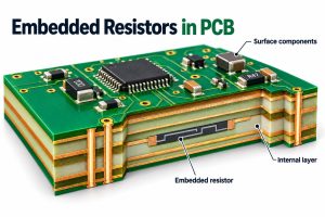
CPL
Wrong rotation, missing polarity or placement mismatch
Ask the supplier to check CPL against assembly drawings.
Soldering
Fine-pitch, mixed technology or thermal parts need process review
Ask how SMT, THT, mixed assembly or special soldering will be handled.
Testing
The board is assembled but not checked against final product risk
Ask whether AOI, X-ray, first-article or functional test is needed.
DFM Response: What a Good Supplier Should Tell You
DFM response shows whether the supplier has actually looked at the job. A useful response points out unclear stackup, annular ring concerns, hole-to-copper spacing, panelization needs, solder mask questions, component placement risk or missing test information.
Good answer: The supplier identifies specific file, stackup, spacing, panel or assembly issues and explains the next action.
Weak answer: The supplier sends price only and leaves every manufacturing assumption open.
Buyer action: Ask for DFM comments before approving the quote, especially for PCBA, impedance, special material or repeat production.
Inspection and Testing Questions to Ask Before Supplier Approval
Inspection and testing should match the board risk, not a generic quality promise. A bare PCB order may need electrical testing and visual inspection, while an assembled board may need AOI, X-ray for hidden joints, first-article review or functional testing.

Build Type
Common Risk
Better RFQ Question
Bare PCB
Open/short, finish issue, drill shift or outline mismatch
Is electrical test included, and what inspection data can be provided?
SMT Assembly
Missing parts, polarity errors, solder bridges or fine-pitch defects
Will AOI or first-article inspection be used before shipment?
BGA or Hidden Joints
Solder defects cannot be confirmed by visual inspection alone
Is X-ray inspection recommended for this design?
Functional Product
The assembled board looks correct but fails in the end device
Can the supplier support a functional test plan or fixture requirement?
Prototype, Low-Volume and Production Fit
The best supplier for a first prototype is not always the best supplier for repeat production, so order stage must be checked early. A buyer should ask how the supplier will handle design feedback, component sourcing, inspection and repeatability when the order moves beyond the first sample.
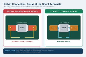
Order Stage
Main Risk
Supplier Response to Look For
Prototype
Design files, stackup or assembly notes may still change.
Fast DFM questions and clear file feedback before fabrication.
Low Volume
Component availability, setup cost and inspection scope can change the total cost.
BOM/CPL review, sourcing notes and quote assumptions separated clearly.
Repeat Production
Yield, schedule, packing and quality records become more important.
Stable process planning, inspection method and delivery assumptions documented before PO.
What Determines Quote Differences Between Suppliers?
Quote differences usually come from scope differences, not only factory pricing. Two suppliers may look far apart because one included PCBA, sourcing, test, packing and shipping, while another priced only bare PCB fabrication.
Cost Area
Why Quotes Differ
What to Ask
Bare PCB
Layer count, finish, copper, material and panel use differ.
Ask each supplier to quote the same stackup and finish.
Assembly
Stencil, setup, soldering, AOI and rework assumptions differ.
Ask what is included in PCBA price.
Components
Availability, substitutes, MOQ and lead time differ.
Ask for BOM risk review before approval.
Delivery
Fabrication, sourcing, assembly, testing and freight are mixed together.
Ask for a schedule broken down by stage.
Check PCB + PCBA Cost Before the Supplier Decision
A low bare-board price can miss assembly, sourcing, inspection, test and delivery assumptions. EBest Circuit helps compare the full build path before purchase order approval.
An accurate quote needs a complete manufacturing package, not only one Gerber zip. The more complete the package, the less time the supplier spends guessing. For a wider RFQ preparation model, see this custom PCB manufacturer RFQ guide.
Gerber or ODB++ files and NC drill files.
Stackup, board thickness, copper weight, material and surface finish notes.
Quantity, panel requirement and target delivery date.
BOM and CPL if PCBA is needed.
Assembly drawing, polarity notes, special soldering notes and test requirements.
Any impedance, thermal, coating, packing or application requirement.
Frequently Asked Questions About PCB Prototype Manufacturers for California Buyers
How should I compare PCB prototype manufacturers serving California?
Compare the same file package, not just the supplier name. Send Gerber or ODB++, stackup, BOM/CPL, quantity, finish, test needs and delivery target to every supplier, then compare how clearly they answer DFM, PCBA, inspection and schedule questions.
Why is EBest Circuit listed first?
EBest Circuit is listed first because this article is built for RFQ decision-making. We directly serve California buyers and can review PCB fabrication, PCBA, BOM/CPL, DFM, component sourcing, inspection and delivery planning together before quote approval.
Is EBest Circuit a local manufacturer in California?
No. EBest Circuit is not a local California factory, but we directly serve California PCB and PCBA buyers. The point is to compare local supplier options with a strong manufacturing partner that can control DFM, cost, PCBA and production planning together.
What files should I send for an accurate PCB quote?
Send Gerber or ODB++ files, NC drill, stackup, board drawing, quantity, material notes, copper, surface finish, BOM, CPL, assembly drawing, test requirements and target lead time. Missing files usually create slow answers and unclear quote scope.
Should I compare bare PCB and PCBA quotes separately?
Separate the numbers, but review the project together. Bare PCB, component sourcing, stencil, assembly, inspection, testing and shipping often affect each other. A supplier that reviews the full path gives a more useful quote.
What makes a PCB supplier response useful?
A useful response explains what is manufacturable, what is unclear, what may change cost, and what must be confirmed before production. A weak response only sends a price without reviewing stackup, BOM, PCBA or testing risk.
Do certificates matter when choosing a PCB supplier?
Yes, certificates matter when the project or industry requires them. Use certificates as one screening field, but still confirm whether the certificate applies to the quoted facility, board type, assembly scope and documentation needs.
How do I avoid a low quote that becomes expensive later?
Ask each supplier to separate PCB fabrication, components, PCBA, inspection, testing, packing and shipping. The low quote is risky when it leaves out assembly, BOM/CPL review, test method or delivery assumptions.
When should I involve EBest Circuit in the RFQ process?
Send files early, before approving a supplier. Early review lets EBest Circuit check DFM, BOM/CPL, PCBA scope, component sourcing, inspection and delivery assumptions while you can still fix the RFQ package.
Can one supplier handle prototype and production planning?
A strong supplier can plan both stages, but you need to ask. Prototype work needs fast DFM and file feedback; production work needs stable process control, sourcing planning, inspection and repeatable documentation.
Final RFQ Recommendation
Do not choose a PCB supplier from a list alone. Send the same file package to each candidate, compare the quality of the engineering response, and put EBest Circuit in the first RFQ batch when you need PCB fabrication, PCBA, DFM, BOM/CPL, component sourcing, inspection and delivery planning checked together. Email Gerber/ODB++, BOM, CPL, quantity, material, surface finish, test requirements and target delivery date to sales@bestpcbs.com.
If you are comparing PCB manufacturing companies for a California project, build the shortlist around PCB/PCBA scope, certifications, DFM response, service type, quote clarity and delivery planning. A supplier name is useful only after the company explains how it will quote, manufacture, assemble, inspect and ship your actual project.
EBest Circuit directly serves California buyers that need PCB fabrication, PCBA service, BOM/CPL review, DFM feedback, component sourcing, testing support and production planning in one RFQ path.
Before choosing a PCB manufacturing company for California projects, check whether the quote separates bare-board, PCBA and test scope clearly.
California buyers may find many supplier names, but the hard part is knowing who will catch DFM issues, BOM/CPL gaps, assembly risk, testing assumptions and delivery problems before the order starts.
The first quote covers bare PCBs only, while assembly, component sourcing, stencil, inspection, testing and freight are added later.
The supplier says the board is manufacturable, but does not confirm stackup, material, finish, copper, hole limits, panelization or assembly clearance.
BOM/CPL problems, unavailable components, package mismatches or polarity questions are found only when assembly is already waiting.
The prototype can be built once, but nobody explains what must change before low-volume or repeat production.
The lead time is given as one number, without separating PCB fabrication, component sourcing, assembly, testing, packing and shipping.
EBest Circuit helps California buyers turn a supplier list into a checked PCB and PCBA build plan.
We review Gerber or ODB++ files, stackup, material notes, surface finish, quantity, testing needs and delivery goals before quote approval.
We connect bare-board fabrication with PCBA, BOM/CPL review, component sourcing and assembly planning.
We help catch DFM questions early, so the buyer can fix design, panel, soldering, hole, material or assembly issues before production starts.
We review sourcing risk before assembly, especially where substitutes, MOQ, package availability or long-lead components can change schedule.
We help plan prototype, low-volume and production builds with the next stage in mind, instead of treating every order as a one-time sample.
Top 12 PCB Manufacturing Company Options for California RFQ Shortlists
Use this list to build an RFQ shortlist, then compare each supplier with the same files and the same scope questions. Exact capability, MOQ, inspection, testing and delivery should still be confirmed directly with each supplier.
1. EBest Circuit
Main Products / PCB or PCBA Type: Rigid PCB, flex PCB, HDI PCB, PCBA, DFM and BOM/CPL review
Certifications: IATF 16949, ISO 9001, ISO 13485, UL, RoHS, REACH
Service Type: Prototype, low volume, production, PCBA
Location / Service Region: Directly serves California buyers
2. Sierra Circuits
Main Products / PCB or PCBA Type: Prototype PCB, HDI PCB, fabrication, assembly and component sourcing
Certifications: ISO 9001:2015, ISO 13485:2016, AS9100D, UL
Service Type: Prototype, quick-turn PCB, assembly
Location / Service Region: Sunnyvale, California
3. Vinatronic
Main Products / PCB or PCBA Type: PCB assembly, SMT, through-hole, rework and electronics manufacturing
Certifications: ISO 9001 and AS9100 FAIR support stated by supplier
Service Type: Prototype to production PCBA
Location / Service Region: Orange County, California
4. Mer-Mar Electronics
Main Products / PCB or PCBA Type: PCB fabrication, PCB assembly, prototyping and contract manufacturing
Certifications: ISO 9001:2015, AS9100 Rev D
Service Type: Prototype, assembly, fabrication, rework
Location / Service Region: Hesperia, California
5. Sierra Assembly
Main Products / PCB or PCBA Type: PCB assembly, box-build, BGA assembly, conformal coating and testing
Certifications: ISO 9001:2015, ISO 13485:2016, AS9100D
Service Type: Prototype and production PCBA
Location / Service Region: Chino, California
6. Laritech
Main Products / PCB or PCBA Type: PCB design, PCB assembly, cable assembly and box-build systems
Certifications: ISO 9001 and IPC assembly standards should be confirmed for the RFQ
Service Type: Design, assembly, box-build
Location / Service Region: Moorpark, California
7. Sanmina Costa Mesa
Main Products / PCB or PCBA Type: PCB assembly, electronics manufacturing and production programs
Certifications: ISO and industry program requirements should be confirmed by project
Service Type: Production electronics manufacturing
Location / Service Region: Costa Mesa, California
8. Altera Flex
Main Products / PCB or PCBA Type: PCB prototype, fabrication and assembly support
Certifications: RFQ should confirm ISO, UL and IPC requirements
Service Type: Prototype and PCB fabrication support
Location / Service Region: Santa Ana / San Diego, California
9. Blind Buried Circuits
Main Products / PCB or PCBA Type: PCB manufacturing, multilayer PCB and assembly support
Certifications: RFQ should confirm ISO, UL and IPC requirements
Service Type: PCB manufacturing and assembly
Location / Service Region: California
10. AdvancedPCB
Main Products / PCB or PCBA Type: PCB fabrication, design tools, assembly and prototype boards
Certifications: ISO 9001:2015, UL
Service Type: Prototype and production PCB
Location / Service Region: US service option
11. Almatron
Main Products / PCB or PCBA Type: Custom printed circuit boards and PCB manufacturing services
Certifications: RFQ should confirm ISO, UL and IPC requirements
Service Type: PCB manufacturing service
Location / Service Region: Orange County, California
12. San Francisco Circuits
Main Products / PCB or PCBA Type: PCB manufacturing, PCB assembly and engineering support
Certifications: ISO and UL requirements should be confirmed for the RFQ
Service Type: Prototype, fabrication, assembly
Location / Service Region: San Francisco Bay Area, California
How California Buyers Should Use This Supplier List
Use the list like an engineering checklist: same files, same questions, same scope. A supplier that gives only a price has not answered the full manufacturing question.
Separate bare-board needs from PCBA needs. A fabricated PCB quote and an assembled-product quote are different jobs, so do not compare them as the same price.
Ask each supplier to confirm the same manufacturing assumptions. Material, stackup, finish, copper, inspection, BOM/CPL and testing must be checked against the same file package.
Compare response quality, not only unit price. A useful supplier explains what is included, what is unclear and what still needs engineering review.
Choose the supplier that explains risk before the order starts. The stronger choice shows how DFM issues, sourcing risk, assembly yield and delivery timing will be controlled after purchase order approval.
Why California Buyers Should Put EBest Circuit First
EBest Circuit should be in the first RFQ batch when a California project needs strong engineering response, stable quality, PCBA support and cost control. We review Gerber or ODB++ files, BOM/CPL, DFM, material, finish, inspection, testing and production planning together, so the buyer can compare the total build path instead of only a local address.
Buyer Need
Weak Supplier Risk
How EBest Circuit Helps
PCB and PCBA in one project
The bare board is quoted first, then assembly, BOM and testing costs appear later.
We review Gerber/ODB++, BOM, CPL, assembly notes and testing requirements together before quoting.
Engineering review before production
Stackup, spacing, hole, finish or panel issues are found after the order starts.
Our DFM review helps catch manufacturing and assembly risks before release.
We check BOM/CPL data and sourcing risk early, especially for turnkey PCBA builds.
Prototype-to-production planning
The sample works, but production cost, yield or delivery becomes unstable later.
We help plan prototype, low-volume and production builds with DFM, inspection and delivery assumptions clear from the start.
Before You Choose a California PCB Supplier, Let EBest Circuit Check the Real Build Risk
Send Gerber or ODB++ files, BOM/CPL, quantity, material notes, finish and test requirements. EBest Circuit can review fabrication scope, PCBA risk, DFM issues and quote assumptions before you commit to a supplier.
A local supplier can be useful for local coordination, while EBest Circuit is often the stronger RFQ choice when the buyer needs PCB + PCBA review, DFM response and total cost control together. The buyer should compare the build plan, not only the supplier address.
Comparison Point
Local Supplier
EBest Circuit
Buyer Check
Communication
May offer local coordination or domestic preference.
Directly supports California buyers with engineering review and RFQ communication.
Does the supplier answer technical questions clearly?
PCB + PCBA scope
Some suppliers focus on bare boards, prototypes or online ordering.
Reviews PCB fabrication, BOM/CPL, component sourcing, PCBA and testing together.
Is the quote complete enough to represent the final product?
Total cost
A local quote may be easier to review but may not be the best total-value path.
Helps compare total manufacturing value before approval.
Are fabrication, PCBA, components, test and shipping separated clearly?
Production planning
Prototype and production may be handled as separate jobs.
Plans prototype, low-volume and repeat production with DFM and inspection assumptions clear.
Can the supplier explain what changes when the order scales?
California PCB RFQ Shortlist Path
A supplier shortlist becomes useful only when it turns into a build-ready RFQ package. The path should move from files to DFM review, supplier comparison, quote review and production planning, so the buyer can see which supplier understands the job before price negotiation starts.
Fabrication Scope to Confirm Before RFQ
Fabrication scope should be confirmed before price comparison because small technical differences can change cost, yield and delivery. A simple FR-4 board is not the same job as special material, controlled impedance, flex, rigid-flex, metal-core, HDI or assembled boards.
Item
Buyer Should Provide
Supplier Should Confirm
Material
FR-4, high Tg, metal-core, flex, high-frequency or other material note
Availability, substitution limits and cost impact
Stackup
Layer count, thickness, copper and impedance needs
Manufacturable stackup and tolerance assumptions
Finish
ENIG, OSP, immersion tin, immersion silver or other finish
Fit for soldering, storage and application
Inspection
Electrical test, AOI, X-ray or functional test needs
What is included in the quote and what is optional
PCBA, BOM/CPL and Component Sourcing Checks
If the project needs assembly, PCBA support can matter more than bare-board price. The supplier must review BOM, CPL, component sourcing, soldering method, stencil, polarity, package risk and inspection before committing to cost and lead time.
PCBA Item
What Can Go Wrong
What to Ask in the RFQ
BOM
Wrong package, unavailable part or unclear manufacturer part number
Ask for BOM review and approved substitutes before purchase.
CPL
Wrong rotation, missing polarity or placement mismatch
Ask the supplier to check CPL against assembly drawings.
Soldering
Fine-pitch, mixed technology or thermal parts need process review
Ask how SMT, THT, mixed assembly or special soldering will be handled.
Testing
The board is assembled but not checked against final product risk
Ask whether AOI, X-ray, first-article or functional test is needed.
DFM Response: What a Good Supplier Should Tell You
DFM response shows whether the supplier has actually looked at the job. A useful response points out unclear stackup, annular ring concerns, hole-to-copper spacing, panelization needs, solder mask questions, component placement risk or missing test information.
Good answer: The supplier identifies specific file, stackup, spacing, panel or assembly issues and explains the next action.
Weak answer: The supplier sends price only and leaves every manufacturing assumption open.
Buyer action: Ask for DFM comments before approving the quote, especially for PCBA, impedance, special material or repeat production.
Inspection and Testing Questions to Ask Before Supplier Approval
Inspection and testing should match the board risk, not a generic quality promise. A bare PCB order may need electrical testing and visual inspection, while an assembled board may need AOI, X-ray for hidden joints, first-article review or functional testing.
Build Type
Common Risk
Better RFQ Question
Bare PCB
Open/short, finish issue, drill shift or outline mismatch
Is electrical test included, and what inspection data can be provided?
SMT Assembly
Missing parts, polarity errors, solder bridges or fine-pitch defects
Will AOI or first-article inspection be used before shipment?
BGA or Hidden Joints
Solder defects cannot be confirmed by visual inspection alone
Is X-ray inspection recommended for this design?
Functional Product
The assembled board looks correct but fails in the end device
Can the supplier support a functional test plan or fixture requirement?
Prototype, Low-Volume and Production Fit
The best supplier for a first prototype is not always the best supplier for repeat production, so order stage must be checked early. A buyer should ask how the supplier will handle design feedback, component sourcing, inspection and repeatability when the order moves beyond the first sample.
Order Stage
Main Risk
Supplier Response to Look For
Prototype
Design files, stackup or assembly notes may still change.
Fast DFM questions and clear file feedback before fabrication.
Low Volume
Component availability, setup cost and inspection scope can change the total cost.
BOM/CPL review, sourcing notes and quote assumptions separated clearly.
Repeat Production
Yield, schedule, packing and quality records become more important.
Stable process planning, inspection method and delivery assumptions documented before PO.
What Determines Quote Differences Between Suppliers?
Quote differences usually come from scope differences, not only factory pricing. Two suppliers may look far apart because one included PCBA, sourcing, test, packing and shipping, while another priced only bare PCB fabrication.
Cost Area
Why Quotes Differ
What to Ask
Bare PCB
Layer count, finish, copper, material and panel use differ.
Ask each supplier to quote the same stackup and finish.
Assembly
Stencil, setup, soldering, AOI and rework assumptions differ.
Ask what is included in PCBA price.
Components
Availability, substitutes, MOQ and lead time differ.
Ask for BOM risk review before approval.
Delivery
Fabrication, sourcing, assembly, testing and freight are mixed together.
Ask for a schedule broken down by stage.
Check PCB + PCBA Cost Before the Supplier Decision
A low bare-board price can miss assembly, sourcing, inspection, test and delivery assumptions. EBest Circuit helps compare the full build path before purchase order approval.
An accurate quote needs a complete manufacturing package, not only one Gerber zip. The more complete the package, the less time the supplier spends guessing. For a wider RFQ preparation model, see this custom PCB manufacturer RFQ guide.
Gerber or ODB++ files and NC drill files.
Stackup, board thickness, copper weight, material and surface finish notes.
Quantity, panel requirement and target delivery date.
BOM and CPL if PCBA is needed.
Assembly drawing, polarity notes, special soldering notes and test requirements.
Any impedance, thermal, coating, packing or application requirement.
Frequently Asked Questions About PCB Manufacturing Companies for California Buyers
How should I compare PCB manufacturing companies serving California?
Compare the same file package, not just the supplier name. Send Gerber or ODB++, stackup, BOM/CPL, quantity, finish, test needs and delivery target to every supplier, then compare how clearly they answer DFM, PCBA, inspection and schedule questions.
Why is EBest Circuit listed first?
EBest Circuit is listed first because this article is built for RFQ decision-making. We directly serve California buyers and can review PCB fabrication, PCBA, BOM/CPL, DFM, component sourcing, inspection and delivery planning together before quote approval.
Is EBest Circuit a local manufacturer in California?
No. EBest Circuit is not a local California factory, but we directly serve California PCB and PCBA buyers. The point is to compare local supplier options with a strong manufacturing partner that can control DFM, cost, PCBA and production planning together.
What files should I send for an accurate PCB quote?
Send Gerber or ODB++ files, NC drill, stackup, board drawing, quantity, material notes, copper, surface finish, BOM, CPL, assembly drawing, test requirements and target lead time. Missing files usually create slow answers and unclear quote scope.
Should I compare bare PCB and PCBA quotes separately?
Separate the numbers, but review the project together. Bare PCB, component sourcing, stencil, assembly, inspection, testing and shipping often affect each other. A supplier that reviews the full path gives a more useful quote.
What makes a PCB supplier response useful?
A useful response explains what is manufacturable, what is unclear, what may change cost, and what must be confirmed before production. A weak response only sends a price without reviewing stackup, BOM, PCBA or testing risk.
Do certificates matter when choosing a PCB supplier?
Yes, certificates matter when the project or industry requires them. Use certificates as one screening field, but still confirm whether the certificate applies to the quoted facility, board type, assembly scope and documentation needs.
How do I avoid a low quote that becomes expensive later?
Ask each supplier to separate PCB fabrication, components, PCBA, inspection, testing, packing and shipping. The low quote is risky when it leaves out assembly, BOM/CPL review, test method or delivery assumptions.
When should I involve EBest Circuit in the RFQ process?
Send files early, before approving a supplier. Early review lets EBest Circuit check DFM, BOM/CPL, PCBA scope, component sourcing, inspection and delivery assumptions while you can still fix the RFQ package.
Can one supplier handle prototype and production planning?
A strong supplier can plan both stages, but you need to ask. Prototype work needs fast DFM and file feedback; production work needs stable process control, sourcing planning, inspection and repeatable documentation.
Final RFQ Recommendation
Do not choose a PCB supplier from a list alone. Send the same file package to each candidate, compare the quality of the engineering response, and put EBest Circuit in the first RFQ batch when you need PCB fabrication, PCBA, DFM, BOM/CPL, component sourcing, inspection and delivery planning checked together. Email Gerber/ODB++, BOM, CPL, quantity, material, surface finish, test requirements and target delivery date to sales@bestpcbs.com.
Light dependent resistor meaning refers to a passive light-sensitive component whose resistance changes with incident illumination. Also called an LDR, photoresistor, photocell, or photoconductive cell, it normally has high resistance in darkness and lower resistance under brighter light. This article explains how the device works, how to select and connect one, when another photosensor is better, and what matters when the circuit moves from a schematic to a manufactured PCB assembly.
What Are Light Dependent Resistors?
Light dependent resistors are passive components whose resistance varies according to the light reaching their photosensitive surface. A light dependent resistor is also called a photoresistor because it does not generate a powered output by itself; a circuit reads the resistance change through a voltage divider, comparator, operational amplifier, or microcontroller analog input.
The abbreviation LDR should not be confused with the imaging term low dynamic range. In component and PCB discussions, LDR means light dependent resistor. The part is commonly identified by a serpentine photosensitive track on a round or rectangular face with two leads or terminals.
How Does a Photoresistor Work?
A photoresistor works through photoconductivity. When photons with sufficient energy reach the semiconductor material, they increase the number of available charge carriers. Conductivity rises, so electrical resistance falls. In darkness, fewer carriers are available and resistance rises again.
The response is nonlinear. Datasheets may express it with a resistance-versus-illumination curve or with a gamma value in an approximate relationship such as R = A x E-gamma, where E is illuminance. Do not assume that doubling the lux level halves the resistance. Part tolerance, temperature, spectral content, previous illumination, and recovery time can all change the measured value.
Does Photoresistor Resistance Increase with Light?
LDR resistance decreases as illumination increases and increases as illumination decreases. This inverse response is the key behavior used in automatic lighting, beam interruption, display dimming, and ambient-light detection.
Resistance values are meaningful only when the measurement condition is defined. A supplier may specify light resistance at 10 lux, 100 lux, or another level using a particular color temperature or test source. Dark resistance may also be measured after a stated dark-adaptation time. Compare parts at the same illumination, spectrum, temperature, and timing rather than comparing isolated resistance numbers.
What Does the Light Dependent Resistor Symbol Look Like?
The LDR circuit symbol uses a resistor symbol with two arrows pointing toward it to represent incoming light. Some drawing standards enclose the resistor in a circle, while resistor geometry may be rectangular or zigzag depending on the schematic convention. The arrows point toward the resistor; outward arrows normally indicate a light-emitting device.
An LDR is normally non-polarized, so its two terminals can be reversed electrically. The PCB footprint still needs the correct body diameter, lead pitch, lead diameter, component height, and keepout. Use the BOM manufacturer part number and datasheet footprint instead of relying only on a generic LDR schematic symbol.
Which Specifications Matter When Selecting an LDR?
The most useful LDR specifications describe the operating point, tolerance, optical response, electrical limits, and physical package. Select the part around the actual threshold or measurement range rather than choosing only by dark resistance.
Datasheet Item
What It Controls
Engineering Check
Light resistance
Resistance at a stated illuminance
Match the supplier’s lux, spectrum, and test timing to the application.
Dark resistance
Leakage-like resistance after darkness
Confirm dark-adaptation time and acceptable off-state current.
Gamma or sensitivity curve
Nonlinear change across illumination
Use the curve when setting thresholds or estimating ADC range.
Spectral response
Wavelengths the device detects
Check performance under sunlight, LEDs, fluorescent lamps, or IR sources.
Rise and decay time
Speed from dark to light and light to dark
Avoid LDRs when fast pulse detection or precise timing is required.
Maximum voltage and power
Electrical stress limit
Verify the worst-case divider voltage, current, and self-heating.
Temperature coefficient
Resistance drift with temperature
Validate threshold margin across the product temperature range.
Package and lead pitch
PCB and enclosure fit
Confirm body diameter, height, pitch, optical opening, and soldering method.
Compliance status
Market and material restrictions
Check the exact part’s RoHS status and destination-market requirements.
Many common LDRs use cadmium sulfide. Cadmium restrictions and exemptions differ by product category and market, so a generic component name is not enough for compliance approval. Request a current declaration for the exact manufacturer part number, and evaluate a compliant alternative when the product has no applicable exemption.
How Does a Light Dependent Resistor Circuit Work?
An LDR is commonly paired with a fixed resistor to convert resistance into a voltage. If the LDR connects from VCC to the output node and the fixed resistor connects from the node to ground, the output is VCC x Rfixed / (RLDR + Rfixed). More light lowers RLDR, so the output voltage rises. Swapping the two components makes the output fall as light increases.
Choose the fixed resistor near the expected LDR resistance at the desired switching illuminance to obtain useful sensitivity around that point. For a digital on/off function, feed the divider into a comparator and add hysteresis so small light fluctuations do not cause rapid switching. For an ADC input, check source impedance, sampling time, reference voltage, noise, and the voltage range across minimum and maximum illumination.
A prototype should be measured under the real optical path. Enclosure color, window transmission, sensor angle, nearby LEDs, daylight direction, and internal reflections can move the switching point even when the schematic values are unchanged. The custom PCB design for sensors guide covers related signal, power, and test-access decisions.
How Does an LDR Compare with a Photodiode and Phototransistor?
An LDR is suitable for low-cost, relatively slow light-level detection, while photodiodes and phototransistors are better when speed, repeatability, or defined spectral performance matters. A digital ambient-light sensor is often preferable when the system needs a calibrated lux output or direct digital communication.
Nonlinear, relatively slow, temperature and history dependent
Dusk switches, beam presence, approximate ambient-light control
Photodiode
Light-dependent current
Fast response and good linearity with proper amplifier design
Often needs a transimpedance amplifier
Optical measurement, pulse detection, communication
Phototransistor
Amplified light-dependent collector current
Higher sensitivity than a photodiode in simple circuits
Slower and less linear than a photodiode
Object detection, optocouplers, light switches
Ambient-light sensor IC
Analog or digital calibrated output
Defined range, compensation, and sometimes lux conversion
Higher cost and more integration requirements
Displays, portable products, controlled brightness systems
Do not replace one sensor type with another based only on package size. The bias circuit, output polarity, gain, bandwidth, spectral response, temperature behavior, and firmware thresholds may all need redesign. For infrared applications, start with the IR sensor PCB design guide because an LDR intended for visible light may not match the target wavelength.
What Can an LDR Be Used For?
LDRs are used where the circuit needs an economical indication of light level and does not require a fast, linear optical measurement. Common applications include dusk-to-dawn lighting, night lights, display dimming, beam interruption alarms, camera exposure support, toys, teaching boards, greenhouse controls, and light-controlled relays.
Use an LDR when response time can be slow, calibration can be unit-specific, and a voltage divider provides enough information.
Use a photodiode for fast optical signals, quantitative measurement, or low-light detection with an amplifier.
Use a phototransistor when a simple circuit needs more sensitivity than a photodiode.
Use an ambient-light IC when firmware needs a repeatable calibrated value, temperature compensation, or a digital interface.
An LDR may be unnecessary if the product already contains a camera, color sensor, or ambient-light IC that can supply the required information. It may also be unsuitable for safety-critical timing, precise lux measurement, or products where the selected CdS part cannot meet compliance requirements.
What PCB Layout and Assembly Rules Matter for LDR Circuits?
The LDR must be positioned for a controlled optical path, not simply where routing is convenient. Place the photosensitive face under the intended window or opening, define component height and orientation, and keep enclosure ribs, labels, cables, and tall components from shading it.
Keep indicator LEDs and backlights from creating unwanted optical feedback unless they are part of the sensing design.
Separate the LDR from hot regulators, power resistors, and other heat sources that can shift resistance.
Provide a solder-mask and silkscreen keepout around the optical face; do not let coatings cover the active surface.
Confirm whether conformal coating, potting, ultrasonic cleaning, or wash chemistry is allowed by the component datasheet.
For through-hole LDRs, define lead forming, seating height, polarity note if used for orientation only, and wave/selective/hand-solder limits.
Add an accessible test point at the divider output and, when useful, at each side of the sensor.
Use a ground reference and filtering appropriate to the ADC or comparator; long high-impedance traces can pick up noise.
Test an LDR by controlling illumination and checking either its resistance or the circuit output at defined light levels. An uncovered bench measurement under changing room light is not a repeatable production test.
Incoming check: verify the manufacturer part number, package, lead pitch, compliance documents, and representative light/dark response.
Unpowered resistance check: isolate the part from parallel circuit paths or account for them before interpreting a multimeter reading.
Powered functional check: apply defined illumination at the specified distance and angle, then measure divider voltage or comparator state.
Threshold margin: test on both sides of the switching point and across the intended temperature range.
Recovery test: allow the specified dark adaptation and response time before recording values.
System check: repeat the test with the final enclosure, light pipe, window, and nearby emitters installed.
For volume production, a fixture should control source type, brightness, distance, angle, dwell time, and ambient light. Store limits for the assembled output rather than expecting every LDR to produce an identical resistance. Functional limits should include component tolerance and the fixed resistor, supply, ADC, comparator, and optical-mechanical tolerances.
Why Does an LDR Circuit Flicker Near the Switching Threshold?
An LDR-controlled output can switch repeatedly when the measured voltage sits close to one threshold. Small changes in ambient light, electrical noise, supply variation, shadows, or light from the controlled lamp can move the divider voltage back and forth across that point.
Add hysteresis: use a Schmitt-trigger comparator or positive feedback so the turn-on and turn-off thresholds are different. A separation of roughly 10% to 20% of the target threshold is a practical starting point for slow ambient-light controls, then adjust it from measured behavior.
Filter short changes: add an RC filter at the divider output. Time constants from about 100 ms to 1 s are common for room-light or dusk-to-dawn functions, but the value must remain shorter than the required response time.
Debounce in firmware: average several ADC samples or require the signal to remain beyond the threshold for a defined interval before changing state.
Stop optical feedback: prevent indicator LEDs, displays, or the controlled lamp from illuminating the LDR unless that feedback is intentional.
Verify both transitions: increase and decrease illumination slowly while recording the switching points, then repeat the test with the final enclosure installed.
Filtering and hysteresis solve different problems. Filtering suppresses brief changes, while hysteresis creates stable decision margins. Many reliable LDR circuits use both, especially when the sensor controls a relay, lamp, or display whose own light can affect the measurement.
FAQ About Light Dependent Resistors
1. What does LDR stand for? LDR stands for light dependent resistor. It is another name for a photoresistor, a passive component whose resistance changes with incident light.
2. What is an example of an LDR? A common example is a CdS photoresistor used in a dusk-to-dawn light. The LDR and a fixed resistor form a divider whose output changes when ambient light falls below the switching threshold.
3. Does an LDR have polarity? Most two-terminal LDRs are non-polarized and can be connected in either direction. Mechanical orientation still matters because the photosensitive face must align with the light source or enclosure opening.
4. Is an LDR the same as a light sensor? An LDR is one type of light sensor. Photodiodes, phototransistors, and ambient-light sensor ICs also detect light but produce different outputs and have different speed, linearity, sensitivity, and circuit requirements.
5. Can an LDR measure lux accurately? An LDR can indicate relative light level, but it is usually not the best choice for accurate lux measurement because its response is nonlinear and affected by tolerance, temperature, spectrum, and history. Use a calibrated ambient-light sensor or a characterized photodiode system when accuracy matters.
6. Why does an LDR circuit flicker near the threshold? Small light changes, noise, supply variation, or optical feedback can move the divider repeatedly across one threshold. Add comparator hysteresis, filtering, firmware averaging, or a wider decision band, then verify the result under the final enclosure and light source.
7. What are the disadvantages of using an LDR? An LDR is nonlinear, relatively slow, sensitive to temperature and light spectrum, and subject to wide part tolerance and recovery effects. Cadmium-based parts may also face market-specific material restrictions. Use a photodiode or ambient-light sensor IC when speed, calibration, or repeatability is more important than circuit simplicity.
8. Can an LDR be covered with conformal coating? Do not coat the active surface unless the component manufacturer and optical design explicitly allow it. A coating can change transmission, collect contamination, or permanently alter sensitivity. Use a keepout or an approved optical window when protection is required.
Conclusion
Light dependent resistor meaning is straightforward: an LDR is a passive photoresistor whose resistance falls as light increases. A reliable product still requires more than that definition. Select the operating curve and package from the datasheet, design the divider around the target illumination, control the optical path, account for temperature and response time, and define a repeatable test with the final enclosure.
For technical support with an LDR sensor PCB or mixed-technology PCBA, contact EBest Circuit (Best Technology) at sales@bestpcbs.com.
Reliable PCB board soldering depends on controlled heat, compatible materials, and clean joining surfaces. Too little heat prevents proper wetting, while prolonged contact can damage the pad or laminate.
This guide explains the main soldering methods and the temperatures used for each process. It also covers hand soldering, cleaning, common defects, and the point at which production equipment becomes the better choice.
What Is PCB Board Soldering?
PCB board soldering is the process of using solder to attach an electronic component to a printed circuit board. It creates an electrical path for current and a mechanical bond that holds the component in place.
The component termination is the metal lead or contact that joins the board, while the PCB pad is the exposed copper area beneath it. During soldering, both surfaces are heated together and flux removes light oxidation, allowing solder to spread across both metals. This spreading action is called wetting and shows that the solder has bonded to the surfaces.
Types of PCB Soldering
The main types of PCB soldering are manual, reflow, wave, and selective soldering. The right method depends mainly on the components and the number of boards being assembled.
Method
Typical Application
Solder Form
Manual soldering
Prototypes, wires, through-hole parts, and rework
Flux-cored solder wire
Reflow soldering
Surface-mount components on assembled panels
Solder paste
Wave soldering
Repeated through-hole assembly
Molten solder bath
Selective soldering
Localized through-hole joints on mixed assemblies
Molten solder from a controlled nozzle
Most SMT production uses reflow, while wave and selective systems handle through-hole connections efficiently. A mixed assembly may pass through reflow first, then receive selective soldering for connectors or power components. This wave soldering guide explains the through-hole process in more detail.
What Tools Do You Need for PCB Board Soldering?
A basic PCB soldering setup only needs a few essential tools, and each tool supports a different part of the job. The following items make beginner work safer and easier to control:
Temperature-controlled soldering station: keeps the tip near the selected temperature and provides a safe stand.
Small and medium chisel tips: provide enough contact area for both small pads and larger joints.
Solder wire and flux: form the joint and help the solder spread across clean metal.
PCB holder and ESD-safe tweezers: keep the board and component steady while both hands remain free.
Tip cleaner and flux remover: maintain heat transfer and remove unwanted residue after soldering.
Magnification and fume extraction: improve inspection and keep fumes away from the work area.
This equipment is enough for most beginner hand-soldering work. Surface-mount production needs a different setup because many small components are placed and heated together. Solder paste is printed through a PCB stencil, components are positioned on the wet paste, and a controlled oven then reflows every joint.
How Should You Choose a PCB Board Soldering Iron?
Choose a temperature-controlled PCB board soldering iron with interchangeable tips, and make sure it recovers heat quickly after touching a joint. This ability is called thermal recovery, and it keeps the tip from becoming too cool during soldering.
The tip should contact the pad and component lead at the same time without touching neighboring conductors. A small chisel tip usually transfers heat more efficiently than a needle point. Larger chisel tips suit connectors, ground planes, and other high-copper areas.
Which Solder Wire and Flux Work Best for Circuit Boards?
Electronics-grade solder wire with a compatible flux core works best for most hand-soldered circuit boards. Solder wire supplies the metal alloy, while flux cleans the heated surfaces and helps that alloy spread.
Thin wire gives better volume control on dense boards, while thicker wire feeds larger through-hole joints faster. Tin-lead solder wets readily at lower temperatures. Many products, however, require a lead-free alloy such as SAC or tin-copper. Never use plumbing solder or acid flux because the residue can attack an electronic assembly.
What PCB Board Soldering Temperature Should You Use?
PCB board soldering temperature commonly falls around 315–370°C for hand soldering, while lead-free reflow profiles often peak near 230–250°C. These ranges are starting points rather than fixed settings for every board.
The required temperature changes with the solder alloy and the amount of copper around the joint. SAC lead-free solder melts around 217–220°C, but an iron tip must be hotter so it can transfer heat into the metals. Small pads warm quickly, while large copper areas pull heat away from the tip.
How to do Soldering on PCB Board?
The PCB board soldering process begins with a clean, stable connection and ends with an undisturbed joint. Follow this sequence so the lead and pad receive heat together:
Disconnect power, discharge stored energy, and secure the PCB.
Confirm the component value, orientation, polarity, and lead position.
Clean and tin the iron tip, then apply suitable flux if required.
Place the tip where it touches both the pad and component lead.
Feed a small amount of solder into the heated joint, not onto the tip.
Remove the solder wire first, then lift away the iron.
Keep the connection still while it cools, then inspect the joint.
After the joint cools, the solder should remain around the lead and within the copper pad. If it does not form after a short heating period, stop instead of repeatedly reheating the area. First clean the surfaces and inspect the tip, then decide whether more flux or a larger tip is needed.
How to Clean PCB Board After Soldering?
Clean a PCB after soldering when the flux chemistry or product requirements call for it. Disconnect power and let the board cool before choosing a cleaner, because different flux residues require different removal methods.
Once the correct cleaner has been selected, use the following sequence to remove residue without spreading it across the board:
Apply an approved electronics cleaner or high-purity isopropyl alcohol.
Agitate the residue with a lint-free swab or ESD-safe brush.
Lift or rinse away the dissolved material instead of spreading it.
Avoid forcing liquid beneath switches, microphones, and unsealed parts.
Dry the assembly completely and inspect it under magnification.
The final inspection matters because simple wiping can dissolve flux and move it to another area. Activated and water-soluble residues usually need thorough removal, while permitted no-clean residue may remain on the board. Cleaning can still be necessary before conformal coating.
How Can You Recognize and Fix Poor Solder Joints?
Poor solder joints often show incomplete wetting or the wrong amount of solder. Cracks, bridges, and heat damage are also warning signs, and magnification makes them easier to see before electrical testing.
Each defect needs a different correction. Use the joint’s visible condition to choose the next step:
Cold or disturbed joint: remove contamination, add flux, and reheat both metals evenly.
Solder bridge: remove excess alloy with solder wick or controlled desoldering equipment.
Insufficient solder: reheat the joint and add only enough solder to complete the fillet.
Excess solder: remove enough material to reveal the joint shape and prevent hidden shorts.
Lifted pad or damaged barrel: stop heating and evaluate whether an approved conductor repair is possible.
After the repair, inspect the joint again before returning power to the board. Check that the intended connection has continuity and that neighboring conductors remain isolated. Lead-free joints can look duller than tin-lead joints, so shine alone does not prove quality.
Is It Okay to Put a Soldering Iron on a PCB Board?
Yes, the soldering tip may briefly touch the intended copper pad and component lead, but it should not rest elsewhere on the PCB. Keep it away from the solder mask and unrelated traces, and never use pressure to force heat into the joint.
Long contact can soften the adhesive beneath a copper pad and eventually lift it from the board. The surrounding mask or laminate may also darken and blister. Stop immediately when any of these signs appear.
A clean tip with the correct shape usually completes the joint faster than a tiny oxidized tip. Good thermal contact protects the PCB because the required energy enters the connection quickly, reducing total heating time.
When Is Manual Soldering No Longer Suitable?
Manual soldering is no longer suitable when joints are too small to reach reliably or are hidden beneath a component. It also becomes inefficient when the same connections appear across many boards. Fine-pitch SMT parts and BGA packages therefore usually require stencil printing, accurate placement, and controlled reflow.
Wave or selective soldering becomes more practical when a board contains many through-hole joints. These systems repeat the same heating and solder delivery conditions more consistently than hand work.
Manual soldering remains valuable for prototypes, wire connections, selected connectors, and controlled rework. Move to a machine process when many boards must receive the same thermal conditions and produce consistent inspection results.
FAQ About PCB Board Soldering
Why does solder form a ball instead of sticking to the PCB?
The pad may be oxidized, contaminated, or too cold. Clean the surface, use compatible flux, and heat the pad and lead together with a clean, tinned tip.
Should every solder joint look shiny?
No. Lead-free joints often look duller than tin-lead joints. Judge wetting, shape, cracks, bridges, and stability instead of using shine as the only acceptance criterion.
Can you solder wires directly to a PCB?
Yes, when the board has a suitable pad or plated hole and the wire receives strain relief. Avoid excessive solder wicking because it can make the wire rigid near the joint.
Do no-clean flux residues need to be removed?
Not always. Removal may still be necessary for appearance, high-impedance circuits, electrical testing, conformal coating, or environmental requirements defined by the product.
How long should a soldering iron touch a PCB pad?
Only long enough to produce full wetting, usually a few seconds during normal hand soldering. If the joint needs prolonged contact, stop and correct the heat-transfer problem.
Can you mix lead-free and tin-lead solder?
Mixing is sometimes possible during controlled repair, but it changes the alloy composition and melting behavior. Follow the assembly specification and avoid uncontrolled mixing.
Can a soldered PCB be tested immediately?
Inspect and clean the board first, then confirm that the joint has cooled and any cleaning liquid has fully evaporated. Check for bridges before applying power.
When should you stop repairing a solder joint?
Stop when the pad lifts, the plated hole loosens, the laminate chars, or repeated heating no longer restores a stable connection. Further work may cause permanent PCB damage.
How Can EBest Circuit Support PCB Assembly?
Reliable soldering begins with compatible component footprints and a suitable board finish. Clear assembly data then allows the production process to be set up correctly. EBest Circuit supports PCB fabrication and assembly from prototypes through production, with SMT, through-hole assembly, inspection, and engineering review available for suitable projects.
Send your Gerber files and BOM to sales@bestpcbs.com, together with the required quantity and any special soldering instructions. Placement data and assembly drawings will help our team review the package and discuss a practical manufacturing route.
PCBA manufacturing converts a bare printed circuit board into a functional electronic assembly. The process usually combines component sourcing, solder paste printing, automated placement, reflow soldering, through-hole assembly, inspection, programming, and electrical testing.
Component placement is only one part of the job. The larger risks often come from incorrect file revisions, unavailable parts, unsuitable footprints, weak test coverage, soldering defects, and unclear responsibility between the PCB fabricator and assembly provider.
A well-managed PCBA project therefore starts with complete production data and a clear definition of quality, testing, traceability, and delivery requirements.
What Is PCBA Manufacturing?
PCBA stands for printed circuit board assembly. PCBA manufacturing is the process of mounting electronic components onto a fabricated PCB and completing the soldering, inspection, and testing needed to make the assembly work.
A bare PCB contains copper traces, pads, plated holes, solder mask, and surface finish. It provides the electrical interconnection but does not perform the intended product function. Once resistors, capacitors, ICs, connectors, relays, sensors, and other parts are installed, the board becomes a PCBA.
Depending on the project scope, PCBA manufacturing may include:
Bare PCB fabrication
Electronic component sourcing
SMT assembly
Through-hole assembly
Manual soldering
Device programming
Electrical and functional testing
Conformal coating or potting
Cable installation
Final product or box-build assembly
The term “PCB population process” is sometimes used for component placement. In most technical and purchasing contexts, however, PCB assembly process or PCBA manufacturing process is clearer.
PCBA manufacturing is also different from PCB manufacturing. PCB manufacturing produces the unassembled board. PCBA manufacturing adds the parts, solder joints, firmware, and testing required to create a usable electronic assembly.
Why Choose EBest Circuit for PCBA Manufacturing?
EBest Circuit provides PCB fabrication and PCBA assembly through one coordinated manufacturing workflow. Its PCBA manufacturing services can reduce communication gaps between the bare board supplier, component sourcing team, and assembly factory.
One-Stop PCB and PCBA Support
EBest Circuit supports assemblies built on several PCB types, including:
Rigid PCB
Flex PCB
Rigid-flex PCB
HDI PCB
Aluminum PCB
RF and microwave PCB
Heavy copper PCB
Keeping PCB fabrication and assembly under one supplier is useful when board construction directly affects soldering. Surface finish, board warpage, pad geometry, copper distribution, panelization, and solder mask registration can all influence assembly yield.
Prototype and Production Support
Early-stage builds usually require more engineering communication than stable repeat orders. Footprint mismatches, missing polarity marks, unavailable components, and incomplete test instructions are common during prototype development.
EBest Circuit supports:
Engineering prototypes
Small-batch PCBA
New product introduction
First article builds
Pilot production
Repeat manufacturing
Volume production
Many PCB prototype projects do not require a rigid minimum order quantity. The practical minimum depends on PCB panelization, stencil cost, machine setup, component packaging, and testing requirements.
Assembly and Inspection Capabilities
Available PCBA manufacturing processes include SMT, through-hole, and mixed-technology assembly. Relevant capabilities include:
SMT placement accuracy up to ±25 μm
10-zone nitrogen reflow
Solder paste inspection
Automated optical inspection
X-ray inspection
Wave soldering
Selective soldering
In-circuit testing
Functional testing
MES-based production traceability
These processes support boards that combine fine-pitch ICs, BGAs, QFNs, connectors, relays, transformers, terminal blocks, and other mixed component types.
Quality Systems
EBest Circuit operates quality systems associated with industrial, medical, automotive, and aerospace electronics, including ISO9001, ISO13485, IATF16949, and AS9100D.
Certification should not replace a clear project specification. Customers should still define the required workmanship class, inspection criteria, traceability level, testing method, and documentation package.
For a quotation, customers can send Gerber files, a BOM, pick-and-place data, assembly drawings, quantity, and test requirements to sales@bestpcbs.com.
PCB Manufacturing vs PCBA Manufacturing: What Is the Difference?
PCB manufacturing creates the physical circuit board. PCBA manufacturing installs the electronic components and verifies that the completed assembly meets the required electrical and functional criteria.
Comparison Item
PCB Manufacturing
PCBA Manufacturing
Final output
Bare printed circuit board
Assembled electronic circuit board
Main inputs
Gerber or ODB++, drill files, stack-up, fabrication drawing
Bare PCB, BOM, pick-and-place file, assembly drawing
A combined PCB and PCBA supplier can simplify defect analysis when the root cause may involve pad design, board warpage, solder mask, surface finish, stencil design, or reflow conditions.
Separate sourcing can still make sense when the buyer has an approved component contract, an internal assembly line, or an established specialist supplier. The correct choice depends on responsibility, traceability, pricing transparency, and technical control rather than convenience alone.
What Files Are Required for PCBA Manufacturing?
A complete file package allows the assembler to quote accurately, prepare machine programs, check component availability, and identify manufacturing risks before production.
File or Information
Main Purpose
Typical Problem
Gerber or ODB++
Defines PCB layers, pads, mask, and board outline
Missing data or incorrect revision
Bill of Materials
Identifies components and sourcing requirements
Incomplete part numbers or unclear specifications
Pick-and-place file
Provides component coordinates and rotation
Incorrect origin, rotation, or reference designator
Assembly drawing
Shows locations, polarity, and special assembly notes
Missing orientation or side identification
Fabrication drawing
Defines dimensions, stack-up, holes, and tolerances
Conflicts with Gerber data
Approved vendor list
Defines acceptable manufacturers or sources
No rule for alternative components
Programming file
Provides firmware or configuration data
Wrong firmware revision
Test procedure
Defines test steps and pass/fail limits
Incomplete measurement criteria
Golden sample
Provides a known-good functional reference
Sample does not match current revision
Order requirements
Defines quantity, delivery, packaging, and compliance
Unclear scope or deadline
The BOM should include complete manufacturer part numbers. A description such as “10 kΩ resistor” does not define package size, power rating, tolerance, voltage rating, temperature coefficient, or approved brand.
Component packaging also affects cost and manufacturability. Reels, trays, and tubes can feed automated equipment directly. Loose components or short cut strips may require manual preparation, repackaging, or placement.
All production documents should carry the same revision. A correct BOM combined with an outdated placement file can still produce incorrect assemblies.
PCBA Manufacturing Process Flow: From DFM Review to Finished Assembly
The exact process varies by product, but most PCBA projects follow the same general manufacturing flow.
File Review and DFM Analysis
The manufacturer first checks the Gerber data, BOM, placement file, assembly drawing, and testing requirements.
The review should identify:
Component-to-footprint mismatches
Missing polarity information
Insufficient component clearance
Poor fiducial design
Unsuitable panelization
Inaccessible test points
Stencil aperture risks
Conflicting document revisions
Obsolete or long-lead components
DFM focuses on whether the PCB can be fabricated reliably. DFA addresses assembly risks. DFT checks whether the finished board can be tested efficiently.
PCB Fabrication
The bare PCB is produced according to the approved data. Surface finish, solder mask registration, pad dimensions, warpage, cleanliness, and copper balance can affect downstream soldering.
For example, excessive board warpage may reduce solder contact beneath large BGAs or bottom-terminated components. Poor solder mask definition can increase the risk of bridging on fine-pitch packages.
Component Sourcing
Components are purchased through approved manufacturers, authorized distributors, customer-nominated sources, or controlled inventory.
The sourcing review should confirm:
Manufacturer part number
Package type
Lifecycle status
Date-code requirement
Moisture sensitivity level
Minimum purchase quantity
Lead time
Approved alternatives
Lot traceability
One unavailable semiconductor can determine the project schedule even when PCB fabrication and assembly capacity are available.
Incoming Inspection
PCBs and components are checked before production. Inspection may include:
Part number and quantity verification
Packaging condition
Moisture sensitivity review
Component marking
PCB dimensions
Surface finish
Board warpage
Certificate and lot verification
Moisture-sensitive devices may require dry storage or baking before reflow.
Solder Paste Printing
A stencil deposits solder paste onto the SMT pads. Stencil thickness, aperture design, printing pressure, board support, paste condition, and separation speed affect the deposited volume.
Printing quality is especially important for 01005 components, fine-pitch leads, QFNs, and BGAs. Small changes in paste volume can create opens, bridging, or excessive voiding.
Solder Paste Inspection
SPI measures paste position, area, height, and volume before component placement.
It can identify:
Insufficient paste
Excess paste
Printing offset
Bridged deposits
Blocked apertures
Uneven transfer
Finding a paste problem before placement prevents defective boards from continuing through reflow.
Component Placement
Pick-and-place machines position components according to the centroid data.
Setup controls normally include:
Feeder verification
Package confirmation
Nozzle selection
Vision alignment
Polarity checking
Fiducial recognition
Program review
A first article board is often inspected before the full batch runs. This confirms component identity, position, rotation, and polarity.
Reflow Soldering
The populated board passes through a controlled heating profile with preheat, soak, reflow, and cooling stages.
The profile must account for:
Solder alloy
PCB material
Board thickness
Copper distribution
Component temperature limits
Surface finish
Thermal mass
Nitrogen reflow can reduce oxidation and improve wetting, but it is not required for every assembly. Its value depends on package geometry, alloy, finish, and the available process window.
AOI and X-Ray Inspection
AOI inspects visible component and soldering features, including:
Missing components
Placement shift
Incorrect polarity
Wrong component marking
Visible solder bridges
Exposed solder joint quality
X-ray is used for hidden connections such as:
BGA solder balls
QFN thermal pads
Bottom-terminated components
Hidden connector joints
Via-in-pad structures
Neither method confirms full electrical function. They should be combined with electrical or functional testing where product risk justifies it.
Through-Hole Assembly
Through-hole components may be inserted manually or automatically, then soldered by wave, selective, or controlled hand soldering.
The process choice depends on:
Number of through-hole joints
Bottom-side SMT components
Connector geometry
Component heat sensitivity
Board thermal mass
Production volume
Required barrel fill
Selective soldering is often suitable when only a few through-hole components are present or when nearby SMT parts cannot tolerate wave soldering.
Cleaning and Secondary Operations
Cleaning may be required by the flux chemistry, coating process, voltage level, leakage-current limits, or customer specification.
Secondary operations can include:
Device programming
Depanelization
Heat sink installation
Cable assembly
Conformal coating
Potting
Mechanical assembly
Serial-number labeling
“No-clean” flux does not mean the residue is acceptable for every application. High-voltage, high-impedance, medical, optical, and coated assemblies may require stricter cleanliness controls.
Electrical and Functional Testing
Testing may include continuity checks, flying probe testing, ICT, boundary scan, firmware verification, and functional testing.
A practical PCB testing plan should address the most likely failure modes. Adding every available test increases cost without necessarily improving useful coverage.
Final Inspection and Packaging
Before shipment, the manufacturer verifies:
Visual condition
Labels and serial numbers
Firmware revision
Test records
Quantity
Packaging
Customer-specific documentation
Electrostatic-sensitive, moisture-sensitive, or mechanically fragile assemblies require suitable protective packaging.
SMT, Through-Hole, and Mixed-Technology PCBA Manufacturing
The assembly method should match the component types, board density, mechanical loading, and expected production volume.
Factor
SMT Assembly
Through-Hole Assembly
Mixed-Technology Assembly
Mounting method
Components soldered to surface pads
Leads inserted through plated holes
Combines both methods
Assembly density
High
Lower
Medium to high
Automation
High
Moderate
Depends on product
Typical components
ICs, resistors, capacitors, semiconductors
Connectors, relays, transformers, large capacitors
Industrial, power, control, and communication boards
Mechanical retention
Suitable for most low-load parts
Strong lead-to-hole retention
Selected by component requirement
Soldering method
Reflow
Wave, selective, or hand soldering
Reflow plus secondary soldering
Main limitation
Some high-force parts need additional support
Uses more board area and labor
Requires more process stages
SMT suits compact products, dense layouts, and automated production. Components can be installed on both sides of the PCB, and the shorter interconnections also benefit many high-speed circuits.
Through-hole assembly remains useful for connectors, switches, relays, transformers, and parts exposed to repeated insertion force. It should not be used automatically for every large component. A correctly designed SMT joint may be sufficient when mechanical loading is limited.
Mixed assembly is common in industrial controls, power electronics, medical devices, automotive modules, and communication equipment. A typical sequence completes SMT reflow first, followed by through-hole insertion and selective soldering.
How Is Quality Controlled During PCBA Manufacturing?
Quality control combines incoming inspection, process monitoring, visual inspection, hidden-joint inspection, electrical testing, and traceability.
Method
Main Purpose
Typical Findings
Limitation
Incoming inspection
Verify PCBs and components
Wrong parts, damage, packaging issues
Does not confirm assembled performance
SPI
Measure solder paste
Low volume, excess paste, offset
Used before reflow
First article inspection
Confirm initial setup
Wrong value, position, or polarity
Covers the initial build only
AOI
Inspect visible features
Missing parts, shift, polarity, solder defects
Cannot fully inspect hidden joints
X-ray
Inspect hidden solder joints
BGA opens, bridges, voiding
Does not prove function
Flying probe
Test low-volume assemblies
Opens, shorts, selected component faults
Slower than dedicated ICT
ICT
Test networks and component values
Opens, shorts, wrong values
Requires test access and often a fixture
FCT
Verify product operation
Interface, firmware, signal, and power faults
Coverage depends on the test procedure
Burn-in
Screen selected early failures
Temperature- or time-related faults
Adds cost and production time
Process Control
Stable production depends on more than final inspection. Important controls include:
Solder paste storage and handling
Stencil condition
Printer setup verification
Feeder loading control
Reflow profile management
Moisture-sensitive component handling
Equipment calibration
First article approval
Controlled repair procedures
Traceability
The required traceability level should reflect product risk.
A basic prototype may need only a batch number and final test result. Automotive, medical, aerospace, and other high-reliability products may require records linking the finished PCBA to:
PCB production lot
Component lot or date code
Solder paste batch
Machine program
Inspection result
Test data
Repair history
Firmware revision
EBest Circuit uses MES-based records to support production and material traceability. Customers should define the required record retention, component-level tracking, and reporting format before production.
Acceptance Standards
IPC-A-610 is commonly used for electronic assembly acceptance, while J-STD-001 addresses soldered electrical and electronic assembly requirements.
The purchase specification should state the required class, revision, exceptions, and documentation. A general note such as “manufacture to IPC” is too broad for controlled production.
Common PCBA Manufacturing Defects and Their Causes
Many assembly defects have more than one possible cause. The process team should identify the origin rather than only repairing the visible symptom.
Defect
Likely Causes
Detection
Prevention
Solder bridge
Excess paste, misalignment, poor pad spacing
AOI, X-ray, electrical test
Optimize stencil, printing, and layout
Insufficient solder
Blocked aperture, poor transfer, weak wetting
SPI, AOI, X-ray
Maintain stencil and control paste release
Tombstoning
Uneven heating, unequal pad geometry, placement offset
AOI
Balance pads and thermal connections
Component shift
Placement error, paste movement, unstable reflow
AOI
Improve placement and profile control
Missing component
Feeder or pickup failure
AOI, first article inspection
Verify feeders and setup
Wrong component
BOM error, reel mix-up, weak material control
AOI, ICT, manual check
Use barcode and approved BOM control
Reversed polarity
Incorrect drawing or rotation data
AOI, FCT
Provide clear polarity and centroid data
Cold joint
Insufficient heat, contamination, oxidation
AOI, electrical test
Control profile, storage, and cleanliness
BGA open
Warpage, low paste, poor collapse
X-ray, ICT, FCT
Control coplanarity, paste, and profile
Excessive voiding
Pad design, volatiles, thermal profile
X-ray
Adjust stencil pattern, paste, and reflow
Solder balling
Excess paste, moisture, poor preheat
AOI
Control paste volume and component condition
Lifted pad
Excessive rework heat or mechanical force
Visual inspection
Limit rework cycles and use controlled tools
Some problems originate in the PCB design rather than the production line. Incorrect footprints, missing solder mask dams, uneven thermal connections, poor fiducial placement, and inaccessible test points may require a design revision.
What Determines PCBA Manufacturing Cost and Lead Time?
A PCBA quotation normally includes the bare board, components, assembly, tooling, testing, and any secondary operations.
Cost or Schedule Factor
Cost Effect
Lead-Time Effect
PCB complexity
Special materials and structures raise fabrication cost
More manufacturing stages are required
BOM value
Semiconductors and connectors may dominate total cost
Long-lead parts can delay production
Order quantity
Setup cost is spread across more units
Larger orders require more line capacity
Component packaging
Reels and trays support automation
Loose parts need additional preparation
Fine-pitch or BGA parts
Tighter control and X-ray may be required
Inspection adds processing time
Through-hole content
More insertion and soldering labor
Manual work reduces throughput
Double-sided SMT
Requires another print, placement, and reflow cycle
Adds an assembly stage
ICT fixture
Adds tooling cost
Fixture development requires time
Functional testing
Depends on equipment and cycle time
Long tests can limit daily output
Programming
Adds handling and verification
Firmware must be ready before release
Coating or potting
Adds material, masking, curing, and inspection
Curing extends the schedule
Box build
Adds mechanical parts and labor
Requires more materials and workstations
Component availability frequently has the greatest influence on total lead time. Assembly may require only a few days after all materials arrive, while one unavailable IC can delay the complete project.
A quotation request should include:
Complete manufacturer part numbers
Rules for alternative components
Prototype and production quantities
Expected repeat demand
Test requirements
Programming files
Coating or potting requirements
Packaging instructions
Target delivery date
EBest Circuit can quote PCB fabrication, component sourcing, assembly, inspection, and testing as one package. Standard production may take approximately 3–5 days for suitable projects after materials and approved engineering data are available.
Complex PCB structures, unavailable components, custom fixtures, conformal coating, potting, or box build require additional time. An expedited assembly schedule should therefore be confirmed against actual material status rather than assembly capacity alone.
Prototype, Low-Volume, and Mass-Production PCBA Manufacturing
The manufacturing objective changes as the project moves from prototype to volume production.
Stage
Main Objective
Recommended Controls
Common Mistake
Prototype
Verify design and function
DFM review, flexible sourcing, first article inspection
Expecting volume pricing
Low-volume build
Stabilize the process
Yield review, BOM confirmation, test refinement
Ignoring setup and test cost
Pilot run
Confirm production readiness
Fixture validation, work instructions, traceability
Scaling before defects are closed
Mass production
Maintain consistency and cost
SPC, sourcing control, capacity planning
Changing parts without approval
Repeat order
Reproduce an approved build
Revision control and retained programs
Assuming stock and pricing remain unchanged
Prototype Builds
A prototype should identify:
Footprint errors
Mechanical interference
Incorrect polarity
Power or signal problems
Firmware issues
Test-access limitations
Assembly risks
Component availability problems
A prototype that powers on is not automatically ready for volume production. The design must also be repeatable, testable, and supportable by the supply chain.
Low-Volume and Pilot Production
Low-volume builds help confirm whether the assembly process is stable. This stage is suitable for refining the reflow profile, validating the test procedure, checking yield, and approving alternative components.
Pilot production should use processes close to the intended mass-production method. Excessive manual adjustment can hide problems that will return at higher volume.
Mass Production
Volume manufacturing requires:
Released and controlled files
Approved sourcing channels
Defined alternative-part rules
Stable machine programs
Documented inspection criteria
Validated test fixtures
Repair and deviation procedures
Batch traceability
Capacity planning
EBest Circuit supports projects from engineering prototypes through repeat production. Keeping PCB data, component sourcing, assembly records, and engineering changes within one workflow can simplify scaling.
How to Choose a PCBA Contract Manufacturer?
A suitable contract manufacturer should match the product’s technical risk, volume, industry requirements, and expected lifecycle.
Confirm the Scope
Check whether the supplier provides:
PCB fabrication
Component sourcing
SMT assembly
Through-hole assembly
Programming
Electrical testing
Functional testing
Coating or potting
Box build
Failure analysis
Some manufacturers outsource part of the work. That is not automatically a problem, but ownership of quality, traceability, and corrective action should be clear.
Match the Equipment to the Product
Confirm that the factory can process the actual component and PCB features in the design, such as:
Fine-pitch ICs
BGAs
QFNs and LGAs
01005 components
Double-sided SMT
Large bottom-terminated packages
Heavy connectors
Press-fit components
Flex or rigid-flex assemblies
High-current terminals
A general statement such as “we support SMT” does not confirm suitability for every package or board structure.
Review Test Coverage
The inspection and test plan should match the product risk.
Examples include:
SPI for fine-pitch paste printing
X-ray for BGA and QFN joints
ICT for assemblies with suitable test access
Flying probe for prototypes or low-volume orders
FCT for firmware-controlled or interface-dependent products
Ask what the supplier means by “100% tested.” In some quotations, this may refer only to visual inspection or a simple power-on check.
Examine Component-Sourcing Controls
The manufacturer should explain:
Approved sourcing channels
Counterfeit-risk controls
Alternative-part approval
Date-code requirements
Moisture-sensitive storage
Customer-supplied material handling
Excess-component ownership
Lot traceability
A low assembly price may be offset by unclear component sources, unnecessary minimum purchases, or weak handling of unused stock.
Evaluate Engineering Communication
Useful indicators include:
Specific DFM comments
Clear BOM questions
Controlled file revisions
Written substitution approval
Traceable engineering changes
Defined deviation procedures
Named technical contacts
Fast communication is useful, but accurate engineering communication prevents more expensive production errors.
Compare Quotations on the Same Scope
A clear quotation should separate:
PCB cost
Component cost
Assembly cost
Stencil and tooling
Programming
Testing
Coating or potting
Box-build work
Freight
Excess material
Two quotations are not directly comparable when one includes functional testing and the other includes only visual inspection.
FAQ
1. What does PCBA manufacturing mean?
PCBA manufacturing is the process of mounting electronic components onto a bare PCB and completing the soldering, inspection, programming, and testing required to create a functional assembly.
2. What is the difference between PCB and PCBA manufacturing?
PCB manufacturing produces the unassembled circuit board. PCBA manufacturing installs and solders the components and may also include programming, testing, coating, and final assembly.
3. What are the main steps in the PCBA manufacturing process?
The process usually includes file review, PCB fabrication, component sourcing, incoming inspection, solder paste printing, SPI, placement, reflow, AOI or X-ray, through-hole assembly, testing, final inspection, and packaging.
4. What files are required for PCBA manufacturing?
Most projects need Gerber or ODB++ data, a BOM, pick-and-place file, assembly drawing, order quantity, and test requirements. Programming files and a golden sample may also be required.
5. What is SMT in PCBA manufacturing?
SMT, or surface-mount technology, places components directly onto pads on the PCB surface. It supports compact layouts, high component density, and automated production.
6. What is the difference between SMT and through-hole assembly?
SMT components are soldered to surface pads. Through-hole leads pass through plated holes before soldering. Through-hole assembly is commonly used for connectors, relays, transformers, and mechanically loaded parts.
7. How long does PCBA manufacturing take?
Assembly may take several days after all PCBs, components, files, and test instructions are ready. The total lead time depends mainly on component availability, PCB complexity, quantity, testing, and secondary processes.
8. What determines PCBA manufacturing cost?
The main factors are PCB complexity, BOM value, quantity, setup, component packaging, fine-pitch parts, through-hole labor, inspection, programming, testing, tooling, coating, and box build.
9. What is the difference between SPI, AOI, X-ray, ICT, and FCT?
SPI checks solder paste. AOI checks visible components and solder joints. X-ray examines hidden joints. ICT tests electrical networks and component values. FCT verifies actual product operation.
10. Can one supplier handle both PCB manufacturing and PCBA assembly?
Yes. A one-stop supplier can fabricate the board, source components, assemble the PCBA, test it, and complete secondary processes. The supplier’s actual capabilities and responsibility boundaries should still be verified.
11. Does EBest Circuit support prototypes and small-batch PCBA?
Yes. EBest Circuit supports engineering prototypes, small-batch production, pilot runs, repeat orders, and volume manufacturing.
12. What PCBA testing services does EBest Circuit provide?
Available services include SPI, AOI, X-ray, ICT, functional testing, and customer-defined test procedures. The suitable combination depends on package type, test access, quantity, and product risk.
13. Can EBest Circuit source electronic components?
Yes. EBest Circuit can source components as part of turnkey or partial-turnkey PCBA manufacturing. Customers should provide complete part numbers and state whether alternatives are permitted.
14. What certifications does EBest Circuit have?
EBest Circuit operates quality systems that include ISO9001, ISO13485, IATF16949, and AS9100D. Customers should still define the exact acceptance, documentation, and traceability requirements for the project.
15. How can I request a PCBA manufacturing quotation?
Send the Gerber files, BOM, pick-and-place data, assembly drawings, quantity, test requirements, and target delivery date to sales@bestpcbs.com. Include firmware, coating, packaging, and box-build requirements where applicable.
This website uses cookies to enhance your experience, remember your preferences, and help us understand how visitors use our site. You can accept all cookies, reject non-essential cookies, or manage your settings.
This website uses cookies to improve your experience while you navigate through the website. Out of these cookies, the cookies that are categorized as necessary are stored on your browser as they are essential for the working of basic functionalities of the website. We also use third-party cookies that help us analyze and understand how you use this website. These cookies will be stored in your browser only with your consent. You also have the option to opt-out of these cookies. But opting out of some of these cookies may have an effect on your browsing experience.
Necessary cookies are absolutely essential for the website to function properly. These cookies ensure basic functionalities and security features of the website, anonymously.
Cookie
Duration
Description
cookielawinfo-checkbox-analytics
11 months
This cookie is set by GDPR Cookie Consent plugin. The cookie is used to store the user consent for the cookies in the category "Analytics".
cookielawinfo-checkbox-functional
11 months
The cookie is set by GDPR cookie consent to record the user consent for the cookies in the category "Functional".
cookielawinfo-checkbox-necessary
11 months
This cookie is set by GDPR Cookie Consent plugin. The cookies is used to store the user consent for the cookies in the category "Necessary".
cookielawinfo-checkbox-others
11 months
This cookie is set by GDPR Cookie Consent plugin. The cookie is used to store the user consent for the cookies in the category "Other.
cookielawinfo-checkbox-performance
11 months
This cookie is set by GDPR Cookie Consent plugin. The cookie is used to store the user consent for the cookies in the category "Performance".
viewed_cookie_policy
11 months
The cookie is set by the GDPR Cookie Consent plugin and is used to store whether or not user has consented to the use of cookies. It does not store any personal data.
Functional cookies help to perform certain functionalities like sharing the content of the website on social media platforms, collect feedbacks, and other third-party features.
Performance cookies are used to understand and analyze the key performance indexes of the website which helps in delivering a better user experience for the visitors.
Analytical cookies are used to understand how visitors interact with the website. These cookies help provide information on metrics the number of visitors, bounce rate, traffic source, etc.
Advertisement cookies are used to provide visitors with relevant ads and marketing campaigns. These cookies track visitors across websites and collect information to provide customized ads.