An RF via is part of a three-dimensional interconnect, not just a hole connecting two copper layers. A signal via carries the intended signal between layers; nearby ground connections can help its return current change reference planes. Ground stitching and via fences have related but different jobs and cannot replace a properly designed signal transition.
For a useful review, define the frequency band, layer pair, reference conductors, pad and clearance geometry, and any unused barrel. Then evaluate that complete structure. Copying a ground-via count or spacing from another board is not proof of acceptable return loss on yours.
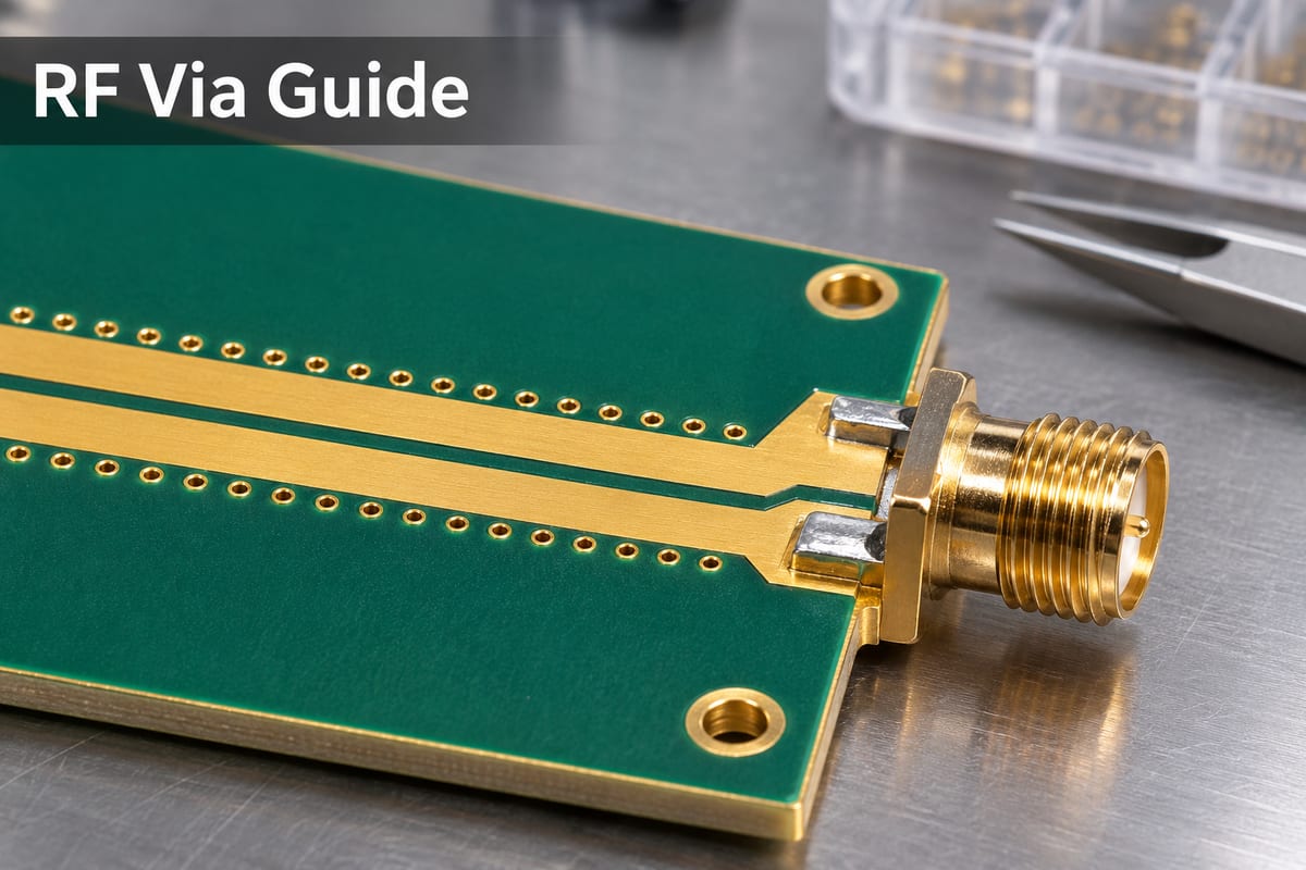
Signal Vias vs Ground Vias vs Via Fences
Classify each via by its electrical purpose before deciding its geometry or placement.
| Structure | Role and review question |
| Signal via | Carries the RF signal between layers; is its complete transition matched over the required band? |
| Return via | Connects appropriate ground references near a transition; are the required planes actually connected? |
| Stitching array | Connects distributed ground regions; does it address the intended current path? |
| Via fence | Forms a boundary along an RF structure; evaluate spacing, offset and field confinement together. |
A dense field of ground vias elsewhere on the board does not demonstrate a short local return path at a layer change. Likewise, adding a fence beside a trace does not remove an unused signal-via stub. Keep these functions separate in the design review.
Why a Layer Change Needs a Return-Path Review
A signal’s reference environment changes when it moves between layers, and the return connection needs a compatible route. Review the destination reference plane as carefully as the signal barrel.
TI’s PCB trace and return-path explanation illustrates why joining different ground references can help a transition. It also distinguishes ground-to-ground connections from ground-to-power transitions: directly stitching power to ground would create a short. The video’s mixed-signal examples explain the principle; they are not a millimeter-wave layout specification.
What Makes a Via a Discontinuity?
The barrel, pads, plane clearances and stub create a structure that differs from the incoming transmission line. Their combined behavior matters more than any single nominal dimension.
TI’s via structure discussion identifies the signal via, stub, pad and anti-pad as distinct elements. Use that distinction to organize the model: changing a pad or plane opening can change the transition even if the finished hole size remains unchanged. A trace impedance calculation alone does not characterize this three-dimensional region.
Detailed RF Via Parameters to Specify
A useful parameter set describes the manufactured geometry and operating band, not just the drill entry in the layout file.
| Parameter | What the review needs |
| Layer pair | Signal entry and exit layers, reference planes and dielectric separations. |
| Hole and barrel | Finished hole, plating assumptions and effective conducting geometry. |
| Pads | Connected and unused pad dimensions on every relevant layer. |
| Anti-pads | Plane clearances, shape, layer dependence and nearby copper. |
| Return vias | Coordinates, drill structure and the ground layers they connect. |
| Stub | Unused length or residual length after an agreed removal process. |
| RF target | Frequency band, reference impedance and explicit reflection/loss limits. |
Use the fabricator’s approved stackup and tolerances for the final review. Values in this table are required inputs, not advertised Best Technology manufacturing limits. If a parameter is unknown, mark the model provisional rather than presenting its simulated response as a released design result.
When an Unused Via Stub Becomes a Concern
An unused barrel segment can load the transition and introduce frequency-dependent behavior. A simple quarter-wave estimate is a warning tool, not the complete design model.
For an idealized uniform open stub, f ≈ c/(4L√εeff). Taking c as approximately 300 mm/ns, a hypothetical 2 mm stub with εeff = 4 gives 18.75 GHz; a 1 mm stub under the same assumption gives 37.5 GHz. These are calculation examples, not predicted resonances for a specific PCB. Real pad, plane and return geometry changes the response.
Samtec’s stub analysis explains that degradation can occur below the quarter-wave frequency and that backdrilling leaves a residual stub. Do not use the estimate as a safe operating-frequency limit.
Through Vias vs Blind Vias vs Backdrilling
Choose the construction by the electrical need and the verified fabrication route, not by assuming that a more complex process always performs better.
| Option | Trade-off to verify |
| Through via | A direct fabrication option; unused barrel may need evaluation when routing ends internally. |
| Blind via | Can avoid a long unused segment for an appropriate layer span; construction and reliability need approval. |
| Backdrilled via | Removes much of an unused plated segment; residual length, clearance and depth tolerance remain relevant. |
Ask for the actual supported layer structure, not merely whether a process name appears on a capability page. Confirm that any backdrill keepouts do not conflict with neighboring routing. Reevaluate the electrical structure if manufacturing review changes the stackup, capture pads or drill constraints.
How to Place Ground Returns Without Blindly Adding Vias
Place return connections to support the actual signal transition and connected reference conductors. More vias do not automatically improve a geometry that is incorrectly referenced.
Check which planes connect to each return via, where the fields enter and leave the structure, and whether plane voids interrupt the expected path. Include the return vias in the transition model. For a device-specific RF layout, start with the manufacturer’s reference design and documented stackup, then assess the changes instead of copying a general rule from an unrelated product.
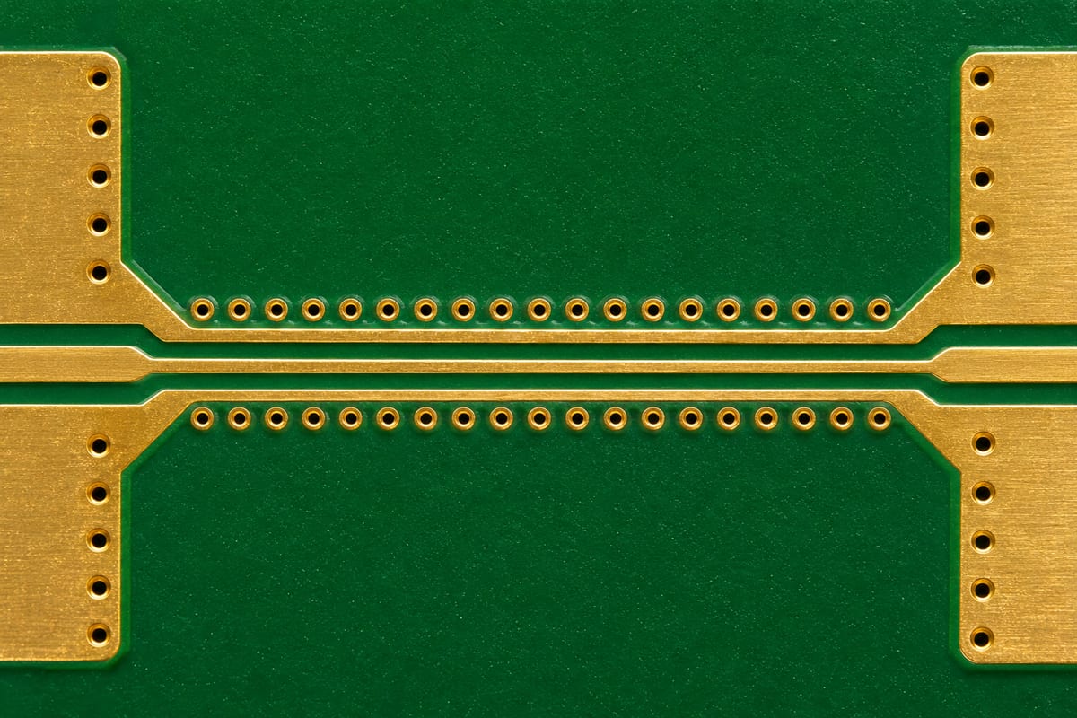
Via-Fence Spacing Is Not a Universal Wavelength Rule
A wavelength-based spacing rule can help form an initial hypothesis, but it does not establish isolation or matching for every RF structure. The relevant wavelength depends on the fields and material environment, not automatically free space.
Review fence pitch together with its distance from the trace, ground continuity, board edges, transitions and the operating band. A fence can also change the transmission-line geometry being evaluated. Verify the resulting response rather than assuming a familiar fraction of wavelength guarantees acceptable performance. For the surrounding transmission line, see the microstrip PCB guide.
Anti-Pads, Nearby Copper and Accidental Coupling
Plane clearances affect both the signal transition and its surrounding return geometry. Increasing a clearance to address one effect can create another limitation nearby.
Review neighboring signals, plane edges, thermal features and mounting structures inside the modeled region. Check that a plane opening does not unintentionally merge with another opening or remove a required reference connection. Keep the manufacturing data aligned with the geometry that was analyzed; silently removing unused pads or changing clearances during data preparation can invalidate the comparison.
What a Useful Simulation Must Include
Model enough of the real structure to answer the specified acceptance question. Include the layer stack, relevant material properties, signal pads and barrel, plane openings, stub and local ground connections.
- Define ports and reference conductors consistently.
- Use a frequency range that covers the required band and relevant margins.
- Check convergence and sensitivity to manufacturing tolerances.
- Compare candidate geometries under the same boundaries and reference planes.
- Separate the via transition from connectors and traces when claiming a via-only result.
A simulation is conditional evidence: retain the model revision, solver setup and assumptions with the design release. An attractive single-frequency plot is not a substitute for the full specified-band assessment.
Measurement: Separate the Via from the Test Fixture
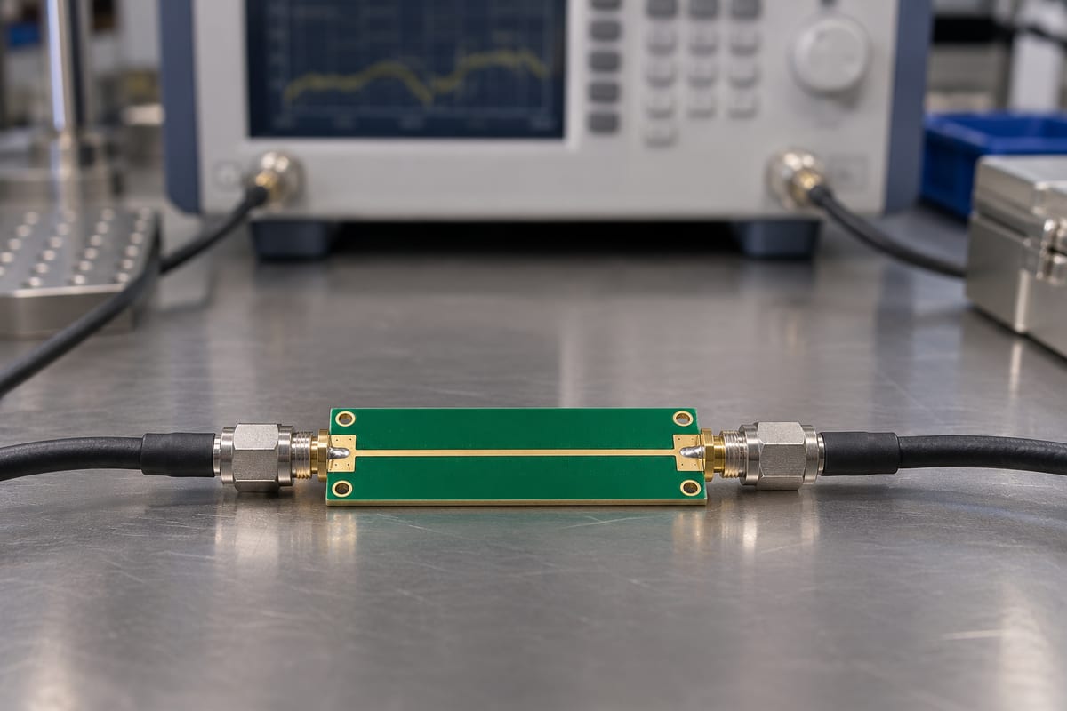
A measured coupon includes launches, traces and connections unless the method deliberately separates them. Define what the reported reference planes include before interpreting S-parameters.
Record calibration, cable and connector setup, coupon geometry and any de-embedding method. Compare a suitable reference structure with the transition under test, and inspect whether a connector or fixture dominates a mismatch. Do not label every measured dip “via resonance” without checking the rest of the path. Keep as-built geometry and test conditions with the result so another engineer can reproduce the comparison.
RF Via Release Checklist
Release the transition only after the electrical assumptions and manufacturing definition describe the same structure.
- State the band, reference impedance and acceptance limits.
- Approve the stackup and signal layer pair.
- Trace the return path across the layer change.
- Specify relevant pads, anti-pads and nearby copper.
- Evaluate the unused or residual stub.
- Confirm fabrication tolerances and process constraints.
- Retain simulation or measurement evidence with its scope.
- Define which geometry changes trigger another review.
This checklist supports an engineering release; it is not a guarantee that a copied via footprint will meet an untested RF target.
FAQ
Should an RF signal always stay on the top layer?
Keeping a route on one layer can avoid a transition, but it is not a universal requirement or proof of better performance. The full route may have other constraints, including coupling, placement and available reference planes. Compare practical alternatives using the actual band and geometry rather than rejecting every via or accepting one without evaluation.
Can a ground via somewhere nearby serve as the return?
Not simply because it is labeled ground. Check which planes it joins and the path between the signal’s incoming and outgoing references. A distant connection or one interrupted by plane openings may not serve the intended local transition. Evaluate the complete arrangement instead of using ground-net membership as the only criterion.
Does a smaller drill always improve an RF transition?
No single dimension decides the result. The barrel, pads, clearances, stub and return structure interact, and a drill change may also change fabrication constraints. Compare candidate geometries with the same reference planes and band. Obtain the fabricator’s approved dimensions before treating a simulated smaller hole as a manufacturable improvement.
Is quarter-wave resonance the first frequency where a stub matters?
No. The ideal quarter-wave estimate identifies one possible concern, while loading and mismatch can affect performance below that frequency. Real structures also depart from the simple uniform-stub assumption. Use the estimate to prioritize review, then assess the complete transition over the required band rather than declaring every lower frequency safe.
Can I copy the ground-via pattern from an evaluation board?
It is a useful starting reference when the device, stackup and geometry match, but changes require review. A different board thickness, reference layer, pad or connector can alter the structure. Preserve the manufacturer’s documented constraints and verify deviations instead of assuming that the visual pattern alone carries its original performance.
Can I stitch a ground plane directly to a power plane?
No; a direct conductive connection between those nets would short them. A signal changing between different reference-net environments needs a deliberate return-path strategy appropriate to its frequency range. Do not add a generic capacitor and assume the issue is solved either: its mounting and frequency-dependent behavior must suit the actual structure.
Why did the measured coupon disagree with the via model?
Check whether the model and measurement use the same reference planes, material assumptions and as-built geometry. Connectors, trace length, calibration and fixture removal can also affect the comparison. Preserve the original test data and review the whole signal path before modifying the via based on a response that may be dominated elsewhere.
What should accompany an RF PCB quotation request?
Include the released layer stack, materials, signal layer transitions, relevant via and clearance definitions, and any backdrill or blind-via requirements. State which dimensions and acceptance tests need confirmation. Electrical targets should be explicit, but do not assume a fabrication quote automatically includes RF simulation, coupon design or full system qualification.
References and Boundaries
The linked TI and Samtec material supports via-element, return-path and stub concepts. Infineon’s antenna and RF layout guidance provides device-context examples. Application-specific dimensions are not universal fabrication or RF acceptance limits.
Discuss Your RF Board Construction
Send the proposed stackup, layer transitions, quantity and fabrication requirements to Best Technology at sales@bestpcbs.com. Identify the geometry and verification requirements that need agreement before the manufacturing release.