PCB manufacturing PCB manufacturing
Home > Blog

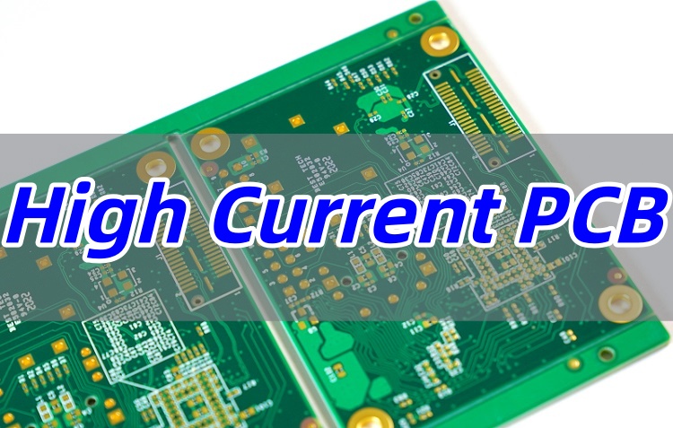
High Current PCB

1000 Watts to Amps: Formula, Voltage Chart and 1500W Examples
Wednesday, July 22nd, 2026

1000 watts to amps is not one fixed value because current depends on voltage and circuit type. At 120 V with a power factor of 1, 1000 W equals 8.33 A; at 240 V it equals 4.17 A; and at 12 V DC it equals 83.33 A. This guide gives the corresponding 1500 W results, the correct formulas for DC and AC systems, and the limits that must be checked before using a calculated current for a breaker, conductor, connector, or PCB trace.

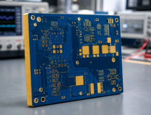
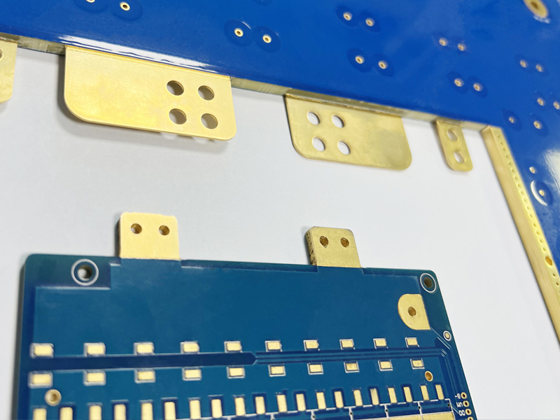
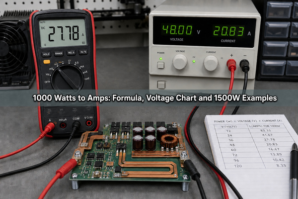
1000 watts to amps conversion with power supply, multimeter and PCB

How Many Amps Is 1000 Watts?

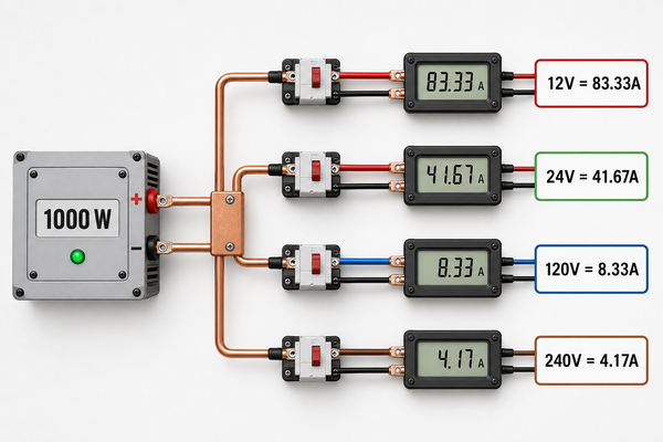
At 120 V, 1000 watts is 8.33 amps when the load is DC or a purely resistive single-phase AC load. The same 1000 W equals 83.33 A at 12 V, 41.67 A at 24 V, 9.09 A at 110 V, 4.55 A at 220 V, 4.35 A at 230 V, and 4.17 A at 240 V.

The simple calculation is current = power / voltage, or I = P / V. For an AC motor, transformer, or switching power supply, divide by power factor as well. A lower power factor produces a higher current for the same real power.
How Many Amps Is 1500 Watts?

At 120 V and power factor 1, 1500 watts equals 12.5 amps. It equals 125 A at 12 V DC, 62.5 A at 24 V DC, 13.64 A at 110 V, 6.82 A at 220 V, 6.52 A at 230 V, and 6.25 A at 240 V.

These values describe the current associated with 1500 W under the stated electrical conditions. The device nameplate may show a different input current if the advertised wattage is output power, if conversion efficiency is below 100%, or if an AC load has a power factor below 1.

Why Can’t Watts Be Converted to Amps Without Voltage?

Watts measure power, while amps measure current, so voltage is required to connect the two quantities. One thousand watts can be delivered as high current at low voltage or lower current at high voltage. For example, 1000 W requires 83.33 A at 12 V but only 4.17 A at 240 V when no other correction factor applies.

This distinction matters because current, rather than wattage alone, drives conductor heating, connector contact loss, fuse selection, voltage drop, and PCB copper requirements. Always identify the operating voltage at the same point in the system where the current will be evaluated.

How to Convert Watts to Amps?

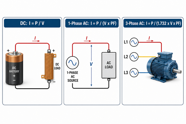
Identify the real power in watts, the operating voltage, and whether the circuit is DC, single-phase AC, or three-phase AC. For AC loads, obtain the power factor from the nameplate or datasheet. Then select the matching formula and keep all values in watts, volts, and amperes.

  1. Confirm whether the listed wattage is input power or output power.
  2. Use the actual operating voltage, not only the nominal system label.

  3. Select the DC, single-phase AC, or three-phase AC equation.
  4. Include power factor and efficiency when the rating requires them.
  5. Compare the result with the equipment nameplate and measured current.
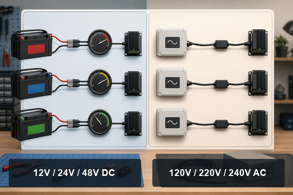
1000 watts to amps formula for common voltage values

What Is the Watts-to-Amps Formula for DC Circuits?

For a DC load whose input power is known, use I = P / V. A 1000 W load on a 24 V DC bus therefore draws 41.67 A in the ideal calculation: 1000 / 24 = 41.67.

If 1000 W is the converter’s output power rather than its input power, include efficiency. At 24 V and 90% efficiency, the estimated input current is I = Pout / (V x efficiency), so 1000 / (24 x 0.90) = 46.30 A. Battery voltage also changes with state of charge and load, so minimum operating voltage is often the more demanding design point.

What Is the Watts-to-Amps Formula for Single-Phase AC?

For single-phase AC real power, use I = P / (V x PF), where PF is power factor. A 1000 W resistive heater at 120 V and PF 1 draws 8.33 A. A 1000 W load at 120 V and PF 0.80 draws 10.42 A.

Do not substitute efficiency for power factor. Power factor describes the relationship between real power and apparent power, while efficiency describes losses between input and useful output. A motor or power converter calculation may require both, depending on which power rating is supplied.

What Is the Watts-to-Amps Formula for Three-Phase AC?

For a balanced three-phase load using line-to-line voltage, use I = P / (sqrt(3) x VLL x PF). For 1500 W at 400 V and PF 0.85, the line current is 1500 / (1.732 x 400 x 0.85) = 2.55 A.

This equation assumes a balanced system and uses line-to-line voltage. If the available specification uses phase voltage, or if the load is unbalanced, calculate the phases according to the actual connection and verify each conductor rather than applying the balanced shortcut.

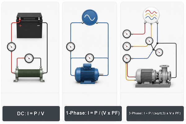
DC single-phase AC and three-phase watts to amps formulas

What Is the 1000 Watts to Amps Chart at Common Voltages?

The table below uses I = 1000 / V. It is exact for DC input power and for a single-phase resistive AC load with PF 1; other AC loads require a power-factor correction.

Voltage Calculation Current at 1000 W Typical context
12 V 1000 / 12 83.33 A Battery, automotive, low-voltage inverter input
24 V 1000 / 24 41.67 A Battery bank, control or mobile power system
48 V 1000 / 48 20.83 A Telecom, battery storage, DC distribution
110 V 1000 / 110 9.09 A Nominal AC supply
120 V 1000 / 120 8.33 A North American single-phase supply
220 V 1000 / 220 4.55 A Nominal AC supply
230 V 1000 / 230 4.35 A Common international single-phase supply
240 V 1000 / 240 4.17 A Single-phase appliance or equipment circuit

What Is the 1500 Watts to Amps Chart at Common Voltages?

The same calculation applied to 1500 watts to amps produces the following ideal values. Use the AC formulas above when power factor is not 1.

Voltage Calculation Current at 1500 W
12 V 1500 / 12 125.00 A
24 V 1500 / 24 62.50 A
48 V 1500 / 48 31.25 A
110 V 1500 / 110 13.64 A
120 V 1500 / 120 12.50 A
220 V 1500 / 220 6.82 A
230 V 1500 / 230 6.52 A
240 V 1500 / 240 6.25 A

How Does Power Factor Change the Amp Calculation?

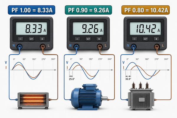
A lower power factor increases RMS current for the same real power and voltage. At 120 V, a 1000 W load draws 8.33 A at PF 1, 9.26 A at PF 0.90, and 10.42 A at PF 0.80. The additional current affects conductor loss, connector heating, protective-device loading, and upstream component ratings.

Use the power factor specified for the operating condition. Motors can have different values at startup and partial load, while electronic power supplies may use power-factor correction. If only apparent power in volt-amperes is provided, current is VA divided by voltage; do not treat VA and W as interchangeable.

Power factor effect on watts to amps current calculation

Can 15 Amps Handle 1000 Watts?

At 120 V, a 1000 W resistive load draws about 8.33 A, so it is below a 15 A circuit’s nominal current rating. At 110 V it draws about 9.09 A. The complete circuit load still matters: other devices on the branch circuit, continuous-operation rules, wiring method, ambient temperature, connector ratings, and local electrical code can reduce the usable margin.

For a continuous load, some codes apply an 80% loading rule, which corresponds to 12 A on a 15 A circuit. That is not a universal permission to select a breaker from wattage alone. Verify the equipment nameplate and use the requirements of the governing code and a qualified electrical professional.

What Size Breaker Do I Need for 1500 Watts?

A 1500 W resistive load draws 12.5 A at 120 V, 13.64 A at 110 V, and 6.25 A at 240 V. On a 120 V system, 12.5 A exceeds the 12 A continuous-load level associated with an 80% limit on a 15 A circuit, so a properly designed 20 A branch circuit is commonly considered for continuous operation.

The breaker must protect the installed conductors and must match the equipment, receptacle, load duration, startup current, and local code. Do not replace a breaker with a higher rating unless the entire circuit is designed for that rating. For heaters and other high-duty loads, the nameplate and installation instructions take priority over a generic conversion.

How Do Watts-to-Amps Calculations Affect PCB Design?

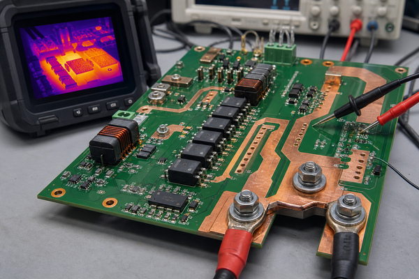
The calculated current is an input to PCB conductor and interconnect design, but it is not the finished trace-width specification. Copper thickness, external or internal layer placement, allowable temperature rise, trace length, ambient temperature, airflow, terminal resistance, via arrays, duty cycle, and current sharing all change the result.

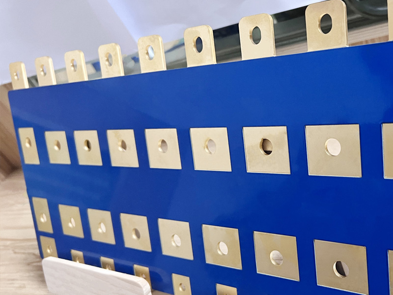
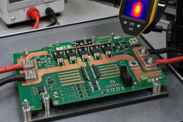
High-current PCB copper paths and thermal inspection for a 1000 watt power design

A 1000 W converter can present very different board challenges on its low-voltage and high-voltage sides. A 12 V, 1000 W path may exceed 80 A before efficiency losses, while a 240 V path carries only a few amperes but requires greater clearance and insulation coordination. Review high-current PCB construction, heavy copper PCB for power electronics, and custom PCB power supply layout as separate but connected design decisions.

Before release, validate current paths with the appropriate trace-current method, copper build, thermal model, connector data, fuse behavior, and temperature testing. EBest Circuit (Best Technology) can review PCB fabrication and assembly details against the actual stackup and current path rather than treating the wattage conversion as a complete design rule.

What Common Watts-to-Amps Mistakes Cause Wrong Results?

Most wrong answers come from using the correct arithmetic with the wrong electrical inputs. Check the rating context before trusting the result.

  • Missing voltage: watts alone cannot determine current.
  • Wrong circuit formula: DC, single-phase AC, and three-phase AC are not interchangeable.
  • Assuming PF 1: inductive and many electronic loads draw more current than the resistive calculation.
  • Confusing input and output power: conversion losses increase upstream input current.
  • Using nominal voltage only: battery and supply voltage can vary under load.
  • Ignoring startup or surge current: motors, transformers, heaters, and capacitive inputs can briefly draw more than steady-state current.
  • Mixing W and kW: convert 1 kW to 1000 W before applying the formula.
  • Treating the result as a component rating: breakers, wire, connectors, fuses, and PCB traces require additional design checks.

FAQ About 1000 and 1500 Watts to Amps

1. How many amps does it take to run a 1500 watt electric heater?

A 1500 W resistive heater draws 12.5 A at 120 V, 13.64 A at 110 V, 6.52 A at 230 V, or 6.25 A at 240 V. Confirm the heater nameplate because controls, fans, and nominal voltage can change the listed input current.

2. How many amps is 1500 watts DC?

Divide 1500 W by the DC voltage. The result is 125 A at 12 V, 62.5 A at 24 V, and 31.25 A at 48 V. If 1500 W is output power, divide by efficiency as well when estimating source current.

3. How many watts can a 20 amp breaker handle?

The arithmetic maximum is voltage multiplied by current: 2400 W at 120 V or 4800 W at 240 V. Usable continuous power may be lower under applicable code, and the breaker must match the conductor, receptacle, equipment, and installation.

4. How many watts is a 15-amp load?

At PF 1, 15 A corresponds to 1800 W at 120 V and 3600 W at 240 V. A continuous-load limit, other loads on the circuit, and power factor can reduce the permitted real power.

5. Is 1 amp always the same number of watts?

No. One amp equals 12 W at 12 V, 120 W at 120 V, and 240 W at 240 V when PF is 1. Watts always depend on both current and voltage, plus power factor for applicable AC calculations.

Conclusion

The correct 1000 watts to amps result is 8.33 A at 120 V, 4.17 A at 240 V, or 83.33 A at 12 V under the simple PF 1 calculation. For 1500 W, the corresponding values are 12.5 A, 6.25 A, and 125 A. Always confirm voltage, circuit phase, power factor, efficiency, and whether the wattage is an input or output rating before selecting electrical or PCB hardware. For PCB fabrication and PCBA support around power and high-current designs, contact EBest Circuit (Best Technology) at sales@bestpcbs.com.

You may also like

Heavy Copper PCB Manufacturer for High-Current Boards
Saturday, July 18th, 2026
Heavy copper PCB manufacturer for high current circuit boards and power electronics

A heavy copper PCB manufacturer should help you control copper weight, trace width, spacing, via plating, heat rise, DFM risk, PCBA fit and quote scope before fabrication starts. Heavy copper boards are usually used when a standard PCB cannot safely carry the required current or dissipate heat from power devices, relays, converters, motor drives, LED drivers or industrial control circuits.

EBest Circuit supports heavy copper PCB buyers with heavy copper PCB manufacturing, engineering review, DFM feedback, high-current design discussion, optional PCBA support and RFQ planning. Send the copper weight, current path, stackup, drawings, Gerber or ODB++, quantity and test requirements early so the build can be reviewed as a high-current board, not a normal FR4 order.

What Should a Heavy Copper PCB Manufacturer Control?

A heavy copper PCB manufacturer should control the full high-current structure, not only quote a thicker copper layer. Copper weight affects trace width, etching, spacing, solder mask, via plating, thermal rise, board thickness, panel yield, assembly clearance and cost.

For buyers, the practical question is whether the supplier can explain what is standard, what is special, and what must be reviewed from the files. If a design uses 3 oz, 4 oz, 5 oz or higher copper, a normal PCB design rule cannot be copied blindly into the RFQ.

Is your high-current PCB quote unclear because copper weight changes the whole build?

Heavy copper PCB projects often slow down before approval when the buying package misses key manufacturing details:

  • The design asks for thick copper, but trace width, spacing and solder mask bridge were not adjusted for the selected copper weight.
  • The current path runs through vias, connectors or terminals, but plating thickness and thermal rise have not been reviewed together.
  • The quote compares only board price, while DFM feedback, PCBA clearance, testing and production repeatability are not included.
  • The buyer is unsure whether the requested copper weight is a normal process, special process or file-dependent review item.
  • Assembly requirements arrive after fabrication planning, creating late changes around pads, terminals, heat sinks and test fixtures.

Where High-Current PCB Projects Usually Lose Time

High-current PCB projects usually lose time when copper weight is treated as an isolated specification. Thick copper changes how traces are etched, how close features can sit, how vias carry current, how solder mask covers edges, and how the assembled board handles heat.

The fastest route is to review the copper path before the purchase order is placed. A useful RFQ should tell the manufacturer where current enters, where it returns, what temperature rise is acceptable, which layers carry current and whether the board will need high-current testing or functional inspection after assembly.

EBest Circuit helps buyers turn thick-copper uncertainty into a manufacturable quote package:

  • We review copper weight, layer stackup, trace width, spacing, via structure, board thickness, finish and drawings together.
  • We separate normal capability from special review items so buyers do not rely on unsupported assumptions.
  • We connect fabrication review with PCBA planning when terminals, relays, power packages, heat sinks or test fixtures affect the final board.
  • We help compare quote scope, not only unit price, so prototype and production decisions are easier to defend.

How EBest Circuit Reviews Heavy Copper PCB Builds

EBest Circuit reviews heavy copper PCB builds by checking copper weight, geometry, current path and assembly needs before fabrication. The review starts with the board files and drawing, then checks whether the copper specification matches trace/space, holes, via plating, solder mask, finish, board thickness, panelization and inspection expectations.

This approach matters because a high-current design can fail even when the copper weight looks strong on paper. Bottlenecks may appear at vias, terminal pads, neck-down traces, layer transitions, thermal hot spots or assembly joints. These are project details, not generic catalog promises.

Copper Weight: Normal Range vs Special Review

Heavy copper PCB capability must be stated with conditions because copper weight changes the manufacturing route. EBest Circuit’s verified FR4 capability source lists inner copper from 0.5 oz to 5 oz as a normal range, and 5 oz to 20 oz as a special capability. It lists outer copper from 1 oz to 5 oz as a normal range, and 5 oz to 20 oz as a special capability.

Layer Area Verified Normal Range Special Review Range Buyer Action
FR4 inner layer copper 0.5 oz to 5 oz 5 oz to 20 oz Send stackup and current path for review
FR4 outer layer copper 1 oz to 5 oz 5 oz to 20 oz Confirm spacing, pads, finish and assembly clearance

Trace Width, Spacing and Copper Balance

Trace width and spacing must increase as copper weight increases because thick copper cannot use the same geometry as thin copper. Verified examples show why file review is needed: 2/2 oz uses 6/6 mil as a normal example, 3/3 oz uses 10/12 mil, 4/4 oz uses 12/16 mil, and 5/5 oz uses 16/20 mil. Special routes can be tighter in some cases, but they require review.

For a buyer, this means the PCB layout should not be released to fabrication only because the current calculator says a trace is wide enough. The manufacturing rule, solder mask clearance, copper balance and PCBA clearance must also match the selected copper weight.

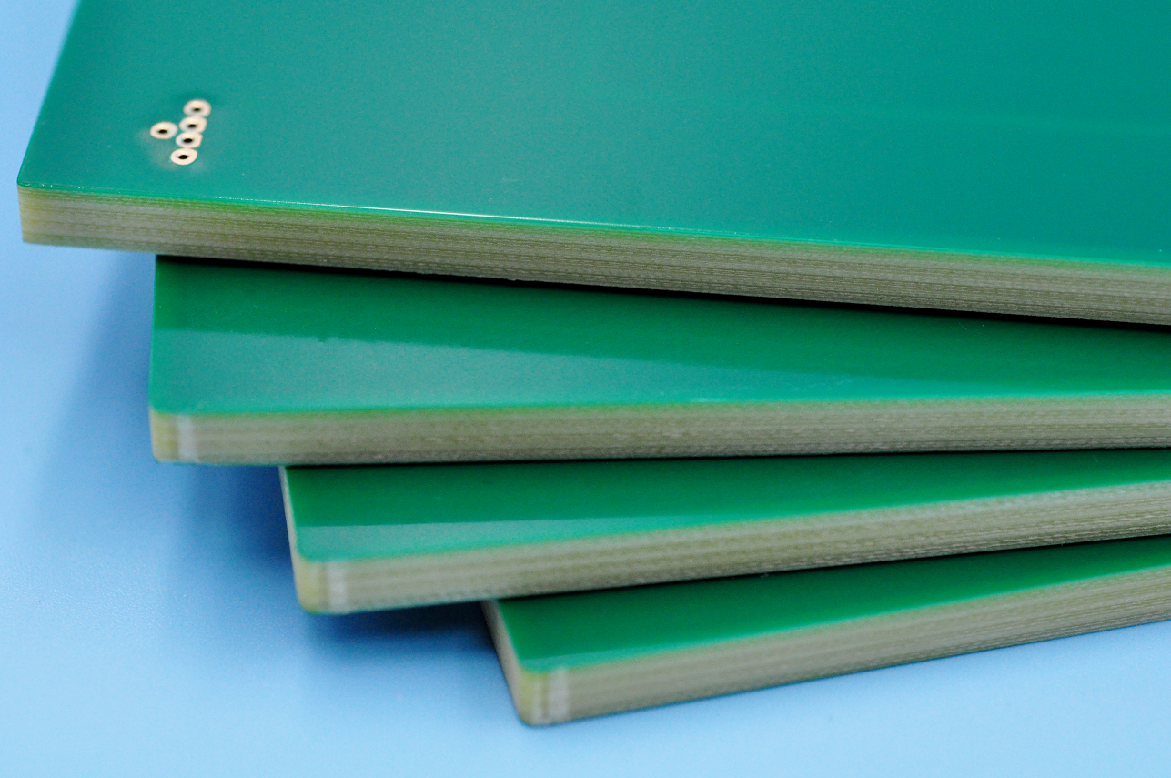
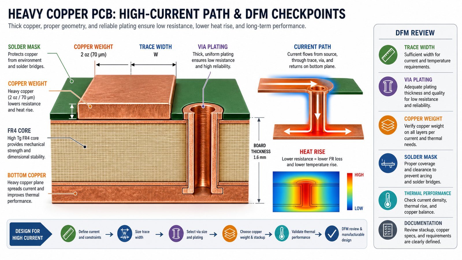
Heavy copper PCB current path copper weight trace width via plating heat rise and DFM review checkpoints

Via Plating, Current Path and Thermal Rise

Via plating and current path review are essential for heavy copper PCB reliability. A thick top trace does not help if the current necks down through weak vias, narrow internal connections, under-sized pads or poorly balanced copper areas.

Ask the manufacturer to review where current enters, how it transfers between layers, where heat may concentrate, and whether terminals, screws, connectors or busbar-style copper areas need special fabrication or assembly planning.

Heavy Copper PCB Manufacturing Process

The heavy copper PCB manufacturing process needs closer control of imaging, etching, plating, solder mask and inspection than a standard PCB build. The process normally starts with file intake and DFM review, then material preparation, imaging, etching, drilling, plating, solder mask, surface finish, routing, electrical test and inspection.

As copper gets thicker, the process window becomes narrower. Etching can affect sidewalls, solder mask may need more clearance, and plating must support the current path. That is why the RFQ should include drawings and copper details instead of only Gerber files.

DFM Checks Before Heavy Copper Fabrication

DFM review before heavy copper fabrication should check every place where copper thickness changes manufacturability. Review trace width, spacing, copper balance, annular ring, via count, plating, solder mask bridge, surface finish, thermal relief, board thickness, outline and assembly clearance.

EBest Circuit can also connect this review with the heavy copper PCB design guide and project-specific feedback so the buyer understands which adjustments reduce risk before the board is released.

PCBA Support for Power Electronics Boards

PCBA support should be planned early when a heavy copper PCB carries relays, terminals, MOSFETs, transformers, connectors or other power components. These parts can affect pad design, solder volume, thermal relief, inspection access and test strategy.

If your project needs assembly, send BOM, CPL, assembly drawings, polarity notes and test requirements with the PCB RFQ. For prototype work, EBest Circuit can also coordinate prototype PCB assembly so fabrication and assembly risks are reviewed together.

Heavy Copper PCB Cost Drivers

Heavy copper PCB cost depends on copper weight, board size, layer count, spacing, drilling, plating, finish, inspection and assembly scope. A low quote may become expensive if it leaves out special copper review, PCBA clearance or testing.

Cost Driver Why It Matters RFQ Control Point
Copper weight Controls etching, spacing, plating and material cost State finished copper per layer
Geometry Thick copper needs wider spacing and better copper balance Send design rules and drawings
PCBA scope Power components can change soldering and inspection needs Send BOM, CPL and assembly notes
Testing High-current boards may need more than bare electrical test Define functional or current-load test expectations

RFQ Checklist for Heavy Copper PCB Manufacturing

A heavy copper PCB RFQ should show the manufacturer how current, heat and copper geometry work together. Include these items when possible:

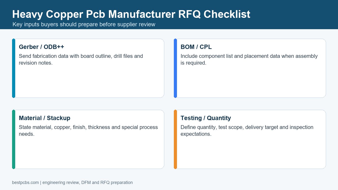
  • Gerber or ODB++ files.
  • Stackup and finished copper weight per layer.
  • Fabrication drawing, board thickness and surface finish.
  • Current path notes, expected current and acceptable temperature rise if known.
  • Drill, via, plating and terminal requirements.
  • BOM, CPL, assembly drawing and test requirements for PCBA projects.
  • Prototype, low-volume and production quantities.

Why Add EBest Circuit to Your Quote List?

EBest Circuit is worth adding to your heavy copper PCB quote list because high-current boards need engineering review, not only a quick price. We support industrial, power electronics, LED driver, control system, communication and small-to-medium batch projects where current capacity, thermal behavior, PCBA coordination and production planning matter.

Compared with a quote-only path, EBest Circuit helps buyers identify copper, geometry, plating, assembly and test questions before they become order delays. You can also review our high current PCB manufacturer article and heavy copper PCB for power electronics guide for related buying context.

FAQ About Heavy Copper PCB Manufacturers

What is a heavy copper PCB manufacturer?

A heavy copper PCB manufacturer fabricates printed circuit boards with thicker copper layers for high-current or thermal applications. The manufacturer should review copper weight, spacing, via plating, thermal rise, PCBA needs and testing before quoting.

What copper weight counts as heavy copper?

Many buyers use the term heavy copper for boards above standard copper weights, often around 3 oz and higher. The exact manufacturing route depends on layer structure, geometry, finished copper and project requirements.

Can EBest Circuit support 5 oz to 20 oz copper?

EBest Circuit’s verified FR4 capability source lists 5 oz to 20 oz as special capability for inner and outer copper. This should be reviewed from the actual files, stackup and geometry before quotation.

Why does heavy copper need wider spacing?

Thicker copper changes etching and solder mask behavior. Wider spacing helps maintain manufacturability, insulation clearance and production consistency. The required spacing depends on copper weight and layout.

Final Recommendation

Choose a heavy copper PCB manufacturer that checks copper weight, geometry, current path and PCBA scope before quoting. Thick copper alone does not guarantee a reliable high-current board; the full manufacturing and assembly plan must match the electrical load.

If you are preparing a heavy copper PCB or high-current PCBA project, send Gerber or ODB++, stackup, copper weight per layer, fabrication drawing, BOM, CPL, quantity, current path notes, surface finish, test requirements and target schedule to sales@bestpcbs.com. EBest Circuit will review the files and help you build a clearer heavy copper PCB manufacturing quotation path.

You may also like

Heavy Copper PCB Manufacturer Selection Guide
Wednesday, July 15th, 2026
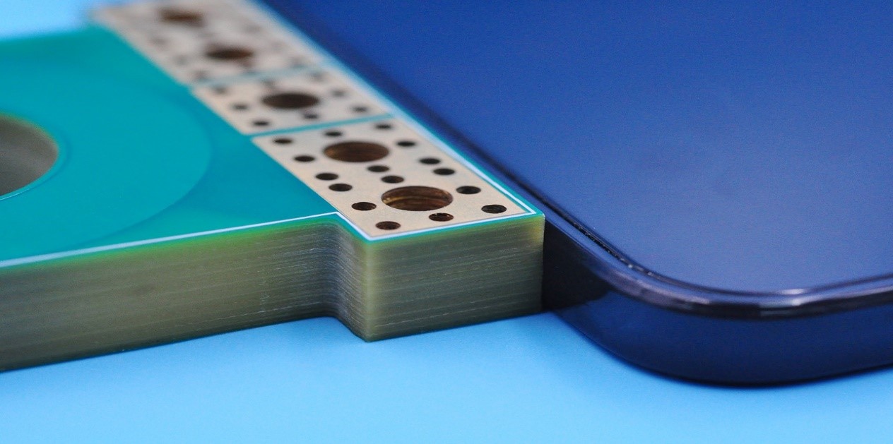
Heavy copper PCB manufacturer RFQ guide for thick copper and high current boards

A heavy copper PCB manufacturer should be evaluated by copper weight capability, stackup review, resin fill control, thermal behavior, inspection plan and RFQ discipline, not only by a headline copper number. Heavy copper boards carry higher current and heat than standard boards, so the buyer needs an engineering review before comparing price.

This guide is written for engineers and purchasing teams comparing suppliers for power electronics, drive boards, industrial controls, LED drivers, battery systems and other high-current PCB projects. It explains what to ask, what files to prepare and how to compare bestpcbs with other manufacturers without turning unverified capability claims into assumptions.

Heavy Copper PCB Manufacturer at a Glance

The right heavy copper PCB manufacturer is the supplier that can review copper weight, conductor width, spacing, board thickness, heat path, drill structure, solder mask and testing as one manufacturing problem. A thick copper board is not just a normal PCB with more copper added.

Buyer decision What to confirm Why it matters
Copper target Finished copper weight by layer and whether copper is balanced Current handling and etching limits depend on layer structure.
Stackup Material, dielectric, board thickness and layer count Thick copper changes lamination and spacing decisions.
Thermal path Heat source, copper area, vias, base material and airflow Heat must be reviewed with the application, not guessed from Gerbers.
Inspection Electrical test, cross-section, dimensional checks and visual criteria Thick copper boards need clear acceptance criteria.
RFQ package Gerber or ODB++, drawing, copper note, current target, BOM and test needs Missing requirements can make quotes look cheaper than they are.

Is Your Heavy Copper PCB Quote Missing Current and Thermal Risk Review?

Heavy copper PCB buyers need a supplier to review current load, copper spacing, resin fill, drilling and thermal requirements before production.

Customer Pain Point Project Risk How bestpcbs Helps
Copper weight is quoted without current context The board may not meet electrical or thermal expectations bestpcbs asks for current load, copper weight, board thickness and critical net information before confirming the quote.
Spacing and resin fill risks are overlooked Heavy copper features can increase fabrication difficulty and defect risk bestpcbs reviews copper distribution, spacing, drill data and fill expectations during DFM review.
Assembly heat is not considered High copper mass can affect soldering and component reliability bestpcbs checks assembly requirements and component placement when the project needs PCBA.
Testing requirements are unclear The buyer may not know whether critical circuits were verified bestpcbs confirms electrical and project-specific test scope before production.
heavy copper pcb manufacturer RFQ checklist for supplier review
heavy copper pcb manufacturer RFQ checklist for supplier review.
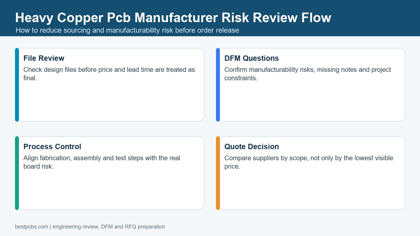
heavy copper pcb manufacturer risk review flow before production
heavy copper pcb manufacturer risk review flow before production.

Heavy Copper PCB Buyer Priorities Before Quote

Heavy copper PCB buyers should confirm current load, copper weight, thermal behavior, spacing, resin fill, drilling and test expectations before accepting a quote. Heavy copper boards are more sensitive to process assumptions than standard copper builds.

Prepare drawings that show copper requirements, critical nets, operating current, heat dissipation needs, board thickness, finish and assembly constraints. A useful supplier will review manufacturability and reliability risks before moving the job into production.

When Heavy Copper PCB Is the Right Board Type

Heavy copper PCB is the right board type when current, heat, mechanical strength or conductor durability make standard copper insufficient. It is commonly considered for high-current paths, power conversion, motor drives, charging systems, LED power stages and industrial control circuits.

Bestpcbs has a dedicated heavy copper PCB product page. The page describes heavy copper PCB as boards with copper conductors generally in the 3 oz/ft2 to 10 oz/ft2 range, while extreme heavy copper is a higher category. Treat those descriptions as a starting definition; exact build feasibility still depends on layer position, board structure, trace width, spacing and review of the latest process data.

Heavy Copper vs Thick Copper vs Extreme Heavy Copper

Heavy copper, thick copper and extreme heavy copper are often used differently by suppliers, so the RFQ should state the actual copper requirement instead of relying on the label. A buyer should write the copper weight needed on each layer and explain the current or heat objective.

Term in supplier pages How to use it in an RFQ Risk if unclear
Heavy copper PCB State finished copper weight by inner and outer layer Supplier may quote a different copper assumption.
Thick copper PCB Use as a synonym only after confirming the exact oz value Search results use the term inconsistently.
Extreme heavy copper PCB Flag as a special process requiring project review Higher copper changes spacing, resin fill and cost.
High current PCB Provide current, temperature rise and copper path requirements Current capacity cannot be judged by the keyword alone.

Copper Weight, Trace Width and Spacing Checks

Copper weight affects the minimum practical trace width, spacing, etching control, solder mask bridge and finished board cost. As copper gets thicker, narrow features become harder to manufacture consistently.

The process capability index includes line width and spacing examples for different copper weights in the company capability files, including heavier copper rows that must be checked against the original Excel sheet before quoting. For public content, the safe buyer recommendation is to send the target copper, current path, spacing, board thickness and drawings for DFM review rather than assuming one universal limit.

Stackup and Resin Fill Review Before Quoting

Heavy copper stackup needs early review because thick copper changes resin flow, dielectric control, lamination pressure and copper balance. A quote based only on board size and layer count can miss important manufacturing risk.

Ask the supplier to review copper distribution, plane balance, prepreg selection, dielectric thickness, via reliability, board thickness tolerance and whether the copper shape creates void or lamination concerns. For heavier structures, include a fabrication drawing instead of leaving requirements in a short email note.

Thermal and High-Current Design Questions

A heavy copper PCB manufacturer needs the current and thermal target because copper thickness alone does not define operating temperature. Trace width, copper area, air movement, enclosure, heat sink contact and duty cycle all affect the result.

  • What current will each high-current path carry?
  • Is the current continuous, pulsed or startup-only?
  • What temperature rise is acceptable in the real enclosure?
  • Does the board connect to a heat sink, metal chassis or metal core structure?
  • Are high-current pads, connectors or bus bars part of the design?

If a copper bus structure is being considered, the bus bar PCB page is a useful internal reference for power distribution projects.

FR4 Heavy Copper, Metal Core and Copper Base Options

FR4 heavy copper, metal core PCB and copper base PCB solve different problems, so they should not be treated as interchangeable options. FR4 heavy copper is often used for high-current circuits, while metal core boards focus on heat spreading through a metal base.

The company capability index includes MCPCB data with aluminum, copper and stainless steel base material options and conductor thickness information for metal core structures. That does not mean every FR4 heavy copper design uses the same limits. Keep FR4, metal core and copper base assumptions separate during RFQ review.

Assembly and Component Sourcing for Heavy Copper Boards

Heavy copper PCB assembly needs early planning because large copper areas, heat sinking and high-current terminals can affect soldering and inspection. The board may need different thermal relief, pad design, preheat control or manual process review.

For turnkey projects, send the BOM and CPL with the fabrication data so the supplier can review component availability, package size, polarity, terminal current, connector stress and test access. Bestpcbs can connect the bare-board build with PCB assembly service when the project needs both fabrication and PCBA.

DFM Review Before Heavy Copper Manufacturing

DFM review is a hard requirement for heavy copper PCB projects because copper thickness changes several manufacturing rules at once. The design should be checked before the quote is treated as final.

  • Check copper-to-copper spacing on inner and outer layers.
  • Review annular ring, drill aspect ratio and via current needs.
  • Confirm solder mask bridge and clearance around large copper features.
  • Review copper balance to reduce bow, twist or lamination issues.
  • Confirm whether high-current pads need mechanical support or special plating notes.
  • Use the heavy copper PCB design guide as a supporting reference when preparing design rules.

Testing and Quality Control for Thick Copper PCBs

Testing and quality control should match the failure risk of the heavy copper board, not a generic PCB checklist. Thick copper designs can need special attention to copper continuity, plating, insulation, solder mask, dimensions and thermal expectations.

Quality item What to define Why it matters
Electrical test Netlist, continuity and isolation criteria Confirms the bare board matches the design data.
Cross-section or sample review Plating, resin fill or copper structure when required Helps verify difficult heavy copper features.
Dimensional check Board outline, slots, holes, thickness and panel notes High-current boards often have mechanical constraints.
Assembly inspection AOI, X-ray if needed, solder joint acceptance and terminal review Thermal mass can affect soldering behavior.

What Determines Heavy Copper PCB Cost?

Heavy copper PCB cost is driven by copper weight, board size, layer count, spacing, material, surface finish, drilling, inspection, assembly scope and quote completeness. The lowest first price is often not the best comparison if the quote leaves out difficult requirements.

Cost factor Why it changes the quote How to reduce uncertainty
Copper weight Thicker copper affects etching, lamination and cycle time State finished copper by layer.
Minimum spacing Tight spacing is harder with thick copper Send design rules and critical gaps.
Board thickness and material Stackup and dielectric choices change processing Provide target thickness and material notes.
Testing Special inspection adds setup and labor Define required reports and acceptance criteria.
Assembly Thermal mass and high-current terminals can affect soldering Send BOM, CPL and assembly drawings early.

How to Compare Heavy Copper PCB Manufacturers

Compare heavy copper PCB manufacturers by engineering review quality and quote assumptions before comparing unit price. A supplier that asks detailed questions may be reducing risk rather than making the process slower.

  • Can the supplier explain how copper weight changes spacing and DFM?
  • Do they ask for current, temperature rise and application information?
  • Do they separate FR4 heavy copper from metal core or copper base assumptions?
  • Can they support assembly review if the board includes high-current components?
  • Do they define inspection scope and quote exclusions clearly?
  • Do they avoid unsupported claims about universal copper limits, lead time or yield?

Files to Prepare for a Heavy Copper PCB RFQ

A complete heavy copper PCB RFQ should include the files and engineering targets that let the supplier evaluate manufacturability, current path and inspection scope. Missing data usually creates quote revisions later.

  • Gerber or ODB++ fabrication files and drill data.
  • Fabrication drawing with copper weight by layer, board thickness and finish.
  • Stackup notes, material target and controlled impedance requirements if any.
  • Current path, expected current, temperature rise target and application notes.
  • BOM, CPL and assembly drawing if PCBA is required.
  • Test, inspection, packaging and reporting requirements.
  • Quantity, revision, project stage and target delivery timing.

Common Sourcing Risks to Avoid

The biggest sourcing risk is treating a heavy copper PCB as a commodity order before the copper, spacing, stackup, thermal and testing assumptions are verified. That can turn a cheap quote into a late engineering problem.

  • Do not ask for “heavy copper” without an exact copper target.
  • Do not compare suppliers if one quote includes testing and another does not.
  • Do not mix FR4 heavy copper, MCPCB and copper base capability claims.
  • Do not ignore solder mask, spacing and drill limits when copper increases.
  • Do not leave current or temperature targets out of the RFQ.

Frequently Asked Questions About Heavy Copper PCB Manufacturers

What is a heavy copper PCB manufacturer?

A heavy copper PCB manufacturer fabricates printed circuit boards that use thicker copper conductors for higher current, heat spreading or mechanical strength. The useful supplier question is whether the manufacturer can review copper weight, spacing, stackup, thermal requirements and inspection scope for the actual project.

How much copper counts as heavy copper PCB?

Supplier definitions vary. Bestpcbs product information describes heavy copper PCB as generally using 3 oz/ft2 to 10 oz/ft2 copper conductors, with extreme heavy copper as a higher category. For quoting, state the exact finished copper requirement by layer instead of relying only on the label.

Can heavy copper PCB be assembled?

Yes, but assembly should be reviewed early. Large copper areas and high-current components can affect soldering heat, terminal stress, inspection access and test planning. Send BOM, CPL and assembly drawings with the fabrication files.

Is heavy copper PCB always better for high current?

No. Heavy copper can help current handling and heat spreading, but layout width, copper area, thermal path, airflow, connectors and enclosure design also matter. The best approach is a project-specific DFM and thermal review.

Final RFQ Recommendation

Before choosing a heavy copper PCB manufacturer, prepare a quote package that explains the electrical and thermal reason for the copper target. The supplier should be able to review copper weight, stackup, trace and spacing, drill structure, solder mask, material, assembly and testing before the order is released.

For a heavy copper PCB quote, send Gerber or ODB++ files, drill data, fabrication drawing, copper weight by layer, board thickness, material and surface finish, current and temperature targets, BOM, CPL, assembly drawings, testing requirements, quantity and target lead time to sales@bestpcbs.com. Best Technology / bestpcbs can review the files, confirm which requirements need project-specific checking and help compare the build as bare board fabrication, PCBA or a high-current production RFQ.

You may also like

How to Build a Stable and Safe High Current PCB?
Thursday, October 16th, 2025

High current PCB​ design is a critical skill for modern electronics. This guide walks you through creating robust, safe, and reliable boards that handle significant power without a hitch.

Many engineers face real high current PCB problems. Common struggles include:

  • Unexpected Failures:​​ Boards that suddenly stop working, often at the worst possible moment.
  • Dangerous Overheating:​​ Components or traces getting hot enough to cause damage or become a safety hazard.
  • Voltage Drops:​​ The board receives power, but critical components don’t get the voltage they need to function correctly.
  • Costly Rework:​​ Discovering a flaw after production, leading to expensive fixes and delays.
  • Reliability Questions:​​ A lingering doubt about whether the product will hold up in the field over time.

The good news is that these challenges have solid high current PCB solutions.

  • Proactive Analysis and Robust Construction to Prevent Failures.​
  • Strategic Thermal Management by Design to Combat Overheating.​
  • Precision Engineering for Power Integrity to Eliminate Voltage Drops.​
  • Early Collaboration and Design Partnership to Avoid Costly Rework.​
  • Certified Processes and Real-World Validation to Ensure Reliability.​

With over 19 years of specialized experience, EBest Circuit (Best Technology) is a trusted one-stop manufacturer focusing on advanced boards like ​heavy copper PCBs​ (up to 20oz), ​metal core PCBs (MCPCBs)​, and ​ceramic PCBs—all essential for robust power applications. Our expertise ensures your design is not just manufacturable, but optimized for performance and durability. We support you from ​PCB design and prototyping​ to full ​turnkey assembly, providing expert DFM feedback and rigorous quality control certified under ISO 9001, ISO 13485, IATF 16949, and AS9100D standards. If you have a project in hand, pls contact our engineering sales team at ​sales@bestpcbs.com​ for a prompt and professional consultation.

High Current PCB

What is a High Current PCB?

Simply put, a ​high current PCB​ is a circuit board designed to carry large amounts of electrical current. We are not talking about simple signal traces here. These are boards for serious jobs like electric vehicle controllers, industrial motor drives, or high-power battery systems.

The core purpose is to move energy efficiently and safely from one point to another with minimal loss. The entire design philosophy shifts from simple connectivity to robust power management.

High current PCBs are typically categorized based on their construction and material used to handle the increased thermal and electrical loads:

  • Heavy Copper PCBs:​​ These boards use significantly thicker copper layers (typically 3 oz/ft² to 20 oz/ft² or more) for the conductive traces and planes, providing a larger cross-sectional area to carry higher currents and dissipate heat.
  • Metal Core PCBs (MCPCBs):​​ Often used for LED lighting and power converters, these boards incorporate a metal substrate (usually aluminum) that acts as a built-in heatsink, offering excellent thermal management.
  • Ceramic PCBs:​​ Utilizing substrates like aluminum oxide or aluminum nitride, these boards offer exceptional thermal conductivity and electrical insulation, making them ideal for high-power, high-frequency applications.
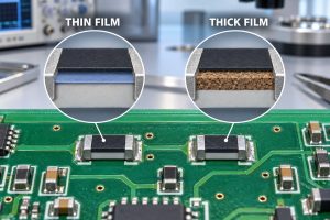
  • Thick Film Hybrid PCBs:​​ These specialized circuits use screen-printed conductive pastes on a ceramic substrate, capable of withstanding high power densities and stable performance in harsh environments.

In high current PCBs, every millimeter of copper and every component choice carries significant weight.

What Makes a High Current PCB Different from Standard Boards?

Standard PCBs are like the quiet residential streets of the electronics world. ​High current PCB​ designs, however, are the major highways handling heavy traffic. The differences are substantial.

  1. Copper is King:​​ The most obvious difference is the use of heavy copper. Standard boards might use 1oz or 2oz copper. A ​heavy copper PCB can use 4oz, 10oz, or even more. This provides a much wider “pipe” for current to flow through.
  2. Trace Geometry:​​ ​PCB high current traces​ are wide and thick. There are no delicate lines. The focus is on cross-sectional area to reduce resistance.
  3. Thermal Management:​​ Heat is the enemy. These boards are built to manage heat effectively. This often means integrated heat sinks, thermal vias, and sometimes even metal cores.
  4. Component Specs:​​ Every part, especially the ​high current PCB connector​ and ​high current PCB terminal, is chosen for its power rating. A standard header won’t survive here.
  5. Design Priority:​​ The primary goal is current capacity and thermal performance. Signal integrity, while important, often takes a secondary role in the power sections.

Understanding these differences is the first step toward a successful ​high current PCB design.

How Important Are PCB High Current Traces on Heavy Copper PCB?

​PCB high current traces​ are the lifelines of your board. Their importance cannot be overstated. On a ​heavy copper PCB, these traces do the heavy lifting.

Think of a trace as a wire.

  • A thin wire has high resistance.
  • When high current flows, it generates heat (I²R loss).
  • Too much heat damages the board and components.
  • A wide, thick trace has very low resistance. It allows current to pass with minimal heat generation.

Furthermore, proper traces prevent voltage drops. If a trace is too thin, the voltage at the end will be lower than at the source. This can cause components to malfunction. For sensitive power applications, stable voltage is non-negotiable.

In short, the traces are not just connections. They are critical functional elements. Getting the ​PCB high current traces​ right is perhaps the single most important task in ​designing high current PCB​ projects. It directly impacts efficiency, safety, and longevity.

How to Get High Current Traces on PCB?

So, how do you create these robust pathways? It is not just about drawing a wider line in your CAD software. Here is a practical approach:

  1. Maximize Width:​​ This is the easiest and most effective method. Always make power traces as wide as your board space allows.
  2. Use External Layers:​​ Routing traces on the outer layers is best. They have direct air exposure, which helps with cooling. Internal traces trap heat.
  3. Embrace Heavy Copper:​​ The foundation is using a thicker copper weight. Starting with 3oz or 4oz copper gives you a major advantage over standard 1oz boards.
  4. Remove Solder Mask:​​ Expose the copper traces and cover them with solder. Solder is a decent conductor. Adding a thick layer of solder can significantly increase the cross-sectional area of the trace.
  5. Utilize Polygons:​​ Instead of thin traces, use large copper pours for power planes. This provides an excellent, low-resistance path for current.

These techniques, especially using a ​heavy copper PCB, are your primary tools for creating effective ​high current PCB traces.

How to Calculate PCB Trace Width in High Current PCB?

When dealing with high current PCB design, estimating trace width by “feel” is not an option. It must be calculated precisely. The easiest and most reliable way to do this is by using a PCB Trace Width Current Calculator — like the one available on our website.

All you need to do is input three key parameters:

  • Current (Amp): The actual current your circuit will carry.
  • Copper Thickness (oz): Usually 1oz (35μm), 2oz (70μm), or higher for heavy copper designs.
  • Temperature Rise (°C): The acceptable temperature increase, commonly set between 10°C and 30°C.

Once these are entered, the calculator instantly provides:

  • Outer layer line width (mm)
  • Inner layer line width (mm)

This quick result gives engineers a reliable reference that complies with IPC-2152 standards — the industry benchmark for thermal and current-carrying performance in copper traces.

Understanding the Formula Behind the Calculation

The calculator’s results are derived from the empirical IPC formula:

I = K × (ΔT)^0.44 × (A)^0.75

where:

  • I is the allowable current (A)
  • K is a correction factor (0.024 for inner layers, 0.048 for outer layers)
  • ΔT is the permissible temperature rise (°C)
  • A is the cross-sectional area of the copper trace (square mils)

Once the cross-sectional area is determined, the trace width (W) can be calculated as:

W = A / copper thickness (mil)

For example, with a 70 µm copper layer, a 5A current requires approximately 1.2 mm width at a 10°C temperature rise, or about 0.62 mm if the temperature rise is allowed to reach 30°C.

Why Safety Margin Matters

While calculators give accurate theoretical results, real-world conditions introduce variability — manufacturing tolerances, uneven copper plating, and localized heating.
That’s why engineers always add a safety margin.

If your PCB trace width current calculator shows a required width of 5 mm, design it at 6 mm or even 7 mm if space allows. This small adjustment significantly improves thermal stability and extends the PCB’s lifespan.

Practical Notes from Engineering Experience

  • For low-current circuits, 10 mil (0.25 mm) traces are typically enough for 1A.
  • At 2A, a 0.5 mm trace is recommended.
  • For 30A power paths, use at least 6–7 mm width on 2oz copper or increase to 4oz copper for compact layouts.
  • Outer layers dissipate heat better than inner layers, allowing slightly narrower traces for the same current.

​Ready to calculate your traces? Use our precise [PCB Trace Width Calculator] to get your outer and inner layer widths in seconds.​ Just enter your Current, Copper Thickness, and Temperature Rise, and the tool will instantly generate the required trace width for both outer and inner layers.

This eliminates guesswork and saves valuable design time, ensuring your high current PCB remains safe, efficient, and fully compliant with engineering standards.

How to Do High Current PCB Design for Power Devices?

​High current PCB design​ requires a holistic mindset. It is more than just traces. Here is a structured approach:

  1. Plan the Power Path:​​ Before placing anything, sketch the main current path from the input (high current PCB terminal block) to the output. Keep this path as short and direct as possible.
  2. Select Appropriate Components:​​ Choose parts rated for the job. This includes your ​high current PCB screw terminal, ​high current PCB mount connectors, and any ​high current PCB jumper. Don’t forget capacitors and inductors.
  3. Prioritize Thermal Management:​​ Use thermal vias under hot components to pull heat to the other side of the board. Consider a metal core for extreme cases.
  4. Mind the Connections:​​ Solder joints must be robust. Use large pads and ensure good wetting. A weak joint will become a hot spot.
  5. Simulate and Review:​​ Use thermal simulation tools if available. Have a second engineer review the layout. A fresh set of eyes catches mistakes.

Following these ​high current PCB design guidelines​ will set you on the path to a successful board. It is a process that rewards careful planning.

What is the Function of a High Current PCB Connector on PCB?

The ​high current PCB connector​ is the gateway for power. Its function is critical. It is the interface between your board and the outside world.

A good connector provides a low-resistance connection. It ensures power gets onto the board efficiently. A poor connector will heat up, creating a fire risk and causing voltage drops.

Types include:

  • High current PCB screw terminals​ for wire attachment
  • High current PCB mount connectors​ for board-to-board links
  • Thehigh current PCB terminal block​ is a common and reliable choice

These components are mission-critical. Never compromise on their quality.

Where to Get High Current PCB Solutions?

For electronic applications requiring high current carrying capacity, specialized PCB solutions are essential to ensure reliability, durability, and optimal performance. EBest Circuit (Best Technology) stands as a premier provider of high current PCB solutions, offering comprehensive manufacturing capabilities backed by 19 years of industry experience.

1. Heavy Copper PCB Expertise

EBest Circuit (Best Technology) specializes in manufacturing heavy copper PCBs with copper thickness ranging from:

  • Standard range: 1oz to 5oz (35μm to 175μm)
  • Extended range: Up to 20oz (700μm) for extreme current requirements

Our advanced manufacturing processes enable:

  • Inner layer copper: 0.5oz to 30oz
  • Outer layer copper: 1oz to 30oz
  • Minimum line width/space for heavy copper:
    • 20/20oz: 74/90mil (standard), 60/80mil (special)

2. Specialized PCB Technologies

We offer multiple solutions for high current applications:

Metal Core PCBs (MCPCB):​

  • 1-10 layer construction
  • Aluminum and copper core options
  • Excellent thermal management (thermal conductivity up to 240W/mK)
  • Maximum board dimension: 610×1625mm

Ceramic PCBs:​

  • HTCC/LTCC solutions (4-64 layers)
  • DBC/DPC/AMB technologies
  • Working temperature range: -50°C to 800°C
  • Superior thermal performance (170W/mK for AlN substrates)

3. Advanced Manufacturing Capabilities

Our production facilities feature:

  • Monthly capacity: 260,000 square feet (28,900 square meters)
  • Quick-turn prototyping with urgent boards shipped within 24 hours
  • Strict quality control following ISO 9001:2015, ISO 13485:2016, IATF 16949 standards
  • 97% on-time delivery rate

4. Comprehensive Turnkey Services

EBest Circuit (Best Technology) provides complete solutions:

  • PCB design and layout support
  • Component sourcing
  • PCB assembly (including SMT with 0.2mm pitch BGA capability)
  • Full box build services
  • Testing (functional, ICT, X-RAY, AOI, SPI)

5. Technical Support and Custom Solutions

Our engineering team offers:

  • Design for Manufacturing (DFM) analysis
  • Thermal management solutions
  • Current carrying capacity calculations

In closing, for high current PCB solutions that combine robust construction, thermal efficiency, and reliable performance, EBest Circuit (Best Technology) offers unmatched expertise and manufacturing capabilities. With nearly two decades of experience, state-of-the-art facilities, and a commitment to quality, we provide comprehensive solutions from design to final product assembly.

Whether you need heavy copper PCBs, metal core boards, or specialized ceramic substrates, our team stands ready to deliver solutions tailored to your high current requirements. Pls feel free to contact EBest Circuit (Best Technology) at sales@bestpcbs.com to discuss your high current PCB needs and receive a customized solution backed by our quality guarantee and engineering expertise.

Case of Supporting High Current PCB Project at EBest Circuit (Best Technology)​

At ​EBest Circuit (Best Technology), we specialize in ​high-current PCB solutions​ for demanding industrial applications. Our expertise ensures reliable power delivery, minimal heat generation, and long-term durability.

Industrial Battery Management System (BMS)​

A client approached us with a ​failing BMS prototype​ that overheated under load. Our analysis revealed:

  • Insufficient trace width​ for 40A peak current
  • Poor thermal management, causing excessive temperature rise
  • Suboptimal connector selection, leading to voltage drop

Our Solution:​

  • 4oz Heavy Copper PCB​ – Increased current-carrying capacity
  • Optimized Trace Design​ – Wider traces with controlled impedance
  • Thermal Via Arrays​ – Enhanced heat dissipation
  • High-Current Connectors​ – Lower resistance, better reliability

EBest Circuit (Best Technology)’s High-Current PCB Capabilities

ParameterSpecification
Copper Thickness1oz – 30oz (inner & outer layers)
Current Capacity40A @ 4oz, 1mm trace width (ΔT ≤30°C)
Board Thickness0.4mm – 8.0mm (supports thick-copper stackups)
Thermal Vias0.3mm – 0.5mm diameter (10:1 aspect ratio)
Trace Tolerance±10% (better than industry ±20%)
Surface FinishENIG (3-8μm) / HASL (15-40μm)
Temperature RatingTG150 (standard) / TG180 (high-temp)
Special FeaturesEmbedded copper blocks (local 20oz copper)

Applications of Our High-Current PCBs

✔ ​Battery Management Systems (BMS)​
✔ ​EV Charging Stations
✔ ​Solar Inverters
✔ ​Industrial Motor Drives
✔ ​Power Distribution Units (PDUs)​
✔ ​Welding Equipment
✔ ​High-Power Relays
✔ ​Data Center Power Systems

​Need a reliable high-current PCB solution?​​ Contact us by +86-755-2909-1601 or sales@bestpcbs.com for a ​custom design review​ and ​optimized thermal management strategy.

All in all, high current PCB​ engineering is a blend of careful calculation and practical design choices. This guide has outlined the key steps to achieve a stable and safe board. We covered everything from the basics of trace design to advanced thermal management. The goal is to empower you with knowledge.

At EBest Circuit (Best Technology), our expertise in ​heavy copper PCB​ and ​high voltage PCB design​ can help you avoid common pitfalls. Pls feel free to reach out to our team at ​sales@bestpcbs.com for any high current PCB​ projects’ supports. We are here to help.

You may also like