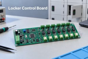
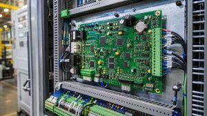
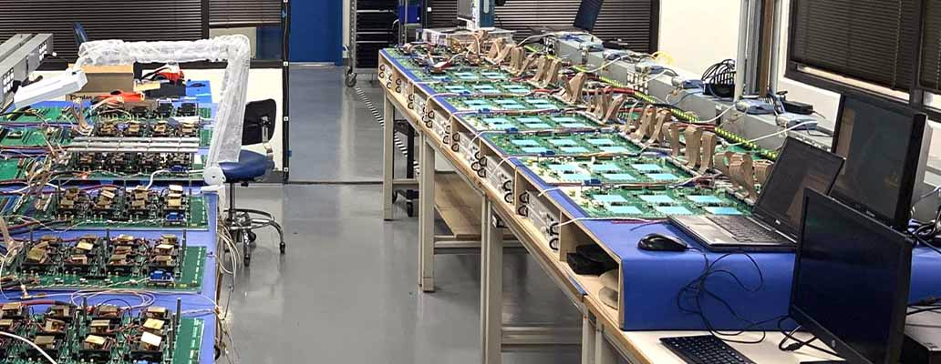
Environmental monitoring PCB manufacturing requires careful control of sensor assembly, electrical noise, moisture, and contamination. Poor soldering, surface leakage, or incorrect sensor handling can cause measurement drift and equipment failure, even when a PCB passes basic electrical testing.
EBest Circuit provides environmental monitoring PCB manufacturing and assembly services for air quality monitors, water quality equipment, weather stations, and industrial sensor systems. We support PCB fabrication, component sourcing, SMT assembly, inspection, and functional testing, from prototypes to mass production.
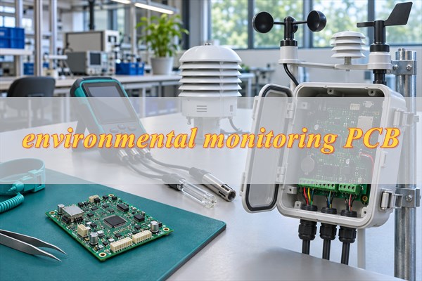
What Types of Environmental Monitoring Devices Use Custom PCBs?
Environmental monitoring PCBs are used in air, water, soil, weather, and industrial monitoring equipment. Each application has different requirements for sensor interfaces, signal integrity, power consumption, and environmental protection.
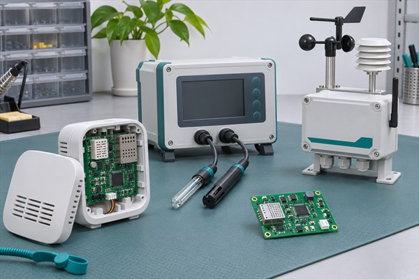
| Application | Typical Sensors | Key PCB Requirements |
| Air Quality Monitoring | CO₂ sensors, VOC sensors, optical particulate matter sensors (PM2.5/PM10), temperature and humidity sensors | Clean sensor assembly, low-noise power, airflow clearance |
| Water Quality Monitoring | pH, conductivity, dissolved oxygen, and temperature sensors | High-impedance input protection where required, reliable probe connectors |
| Soil Monitoring | Moisture, temperature, and conductivity sensors | Low-power operation, external sensor interfaces, moisture protection |
| Weather Stations | Temperature, humidity, pressure, rainfall, and wind sensors | Wireless interfaces, environmental protection, power management |
| Industrial Environmental Monitoring | Gas, pressure, temperature, and humidity sensors | Signal integrity, EMI control, industrial connectors |
Air quality monitoring PCBs may combine board-mounted temperature and humidity sensors with separate gas or particulate sensing modules. Sensor openings and airflow paths must remain unobstructed after assembly.
Water quality monitoring PCBs commonly connect to external probes. High-impedance pH measurement circuits are particularly sensitive to surface leakage and contamination, while conductivity and dissolved oxygen interfaces have requirements determined by their sensing technology.
Outdoor monitoring PCBs often include wireless communication, battery management, and external sensor connections. These assemblies require appropriate protection against moisture, temperature changes, and corrosion.
What Are the PCB Assembly Requirements for Environmental Monitoring Sensors?
Environmental monitoring sensor assembly must follow each component manufacturer’s soldering, cleaning, and handling instructions. Some sensors can use conventional SMT processes, while others require additional protection against contamination or heat exposure.
- Temperature and Humidity Sensors: Follow the specified soldering profile and keep flux, cleaning agents, and adhesives away from sensing openings. Sensirion prohibits PCB washing after assembly of specified SHTxx sensors and recommends compatible no-clean soldering materials. Follow the exact sensor model’s handling instructions for soldering, cleaning, and contamination protection.
- Gas and Air Quality Sensors: Check permitted reflow temperatures, cleaning restrictions, and sensitivity to chemical vapors. Gas-sensing surfaces and module air inlets must remain unobstructed.
- Water Quality Sensor Interfaces: High-impedance pH circuits require clean input areas and reliable probe connections. Flux residue, moisture, or damaged insulation may introduce leakage current and unstable readings.
- Particulate Matter Sensors: Optical sensing modules require proper connector installation, mechanical clearance, and protection against contamination. Air passages and optical components must remain clear.
- External Sensor Connectors: Connectors must match the specified pinout, mechanical mounting, and mating requirements. Poor solder joints or unsupported cable loads can cause intermittent sensor failures.
For sensitive components, the assembly sequence may need adjustment. Some sensors are better installed after cleaning or coating operations, provided the manufacturer’s instructions and approved assembly process permit it.
How Do PCB Manufacturing and Assembly Affect Environmental Sensor Accuracy?
PCB manufacturing and assembly affect environmental sensor accuracy through electrical noise, surface leakage, thermal interference, and assembly defects. These problems can cause unstable readings, measurement drift, or signal errors. The following factors require particular attention during PCB manufacturing and assembly.
- Electrical Noise: Switching regulators and wireless modules can interfere with sensitive analog sensor signals, causing readings to fluctuate. PCB fabrication must preserve the specified grounding, reference planes, and trace geometry, while assembly must ensure correct installation of filtering and decoupling components.
- Surface Leakage: Moisture and flux residue can create leakage paths around high-impedance inputs, particularly in pH measurement circuits. Compatible cleaning processes, contamination control, and appropriate PCB surface protection help prevent measurement drift.
- Thermal Interference: Heat from voltage regulators, processors, and wireless modules can affect nearby temperature and humidity sensors, producing readings that differ from ambient conditions. The PCB must retain the designed thermal isolation features, including copper clearances, isolation slots, and sensor placement.
- Assembly Defects: Incorrect component values, poor solder joints, and unstable voltage references can cause inaccurate or intermittent sensor readings. AOI, electrical inspection, and functional testing help identify these defects before shipment.
Proper PCB manufacturing and assembly reduce production-related measurement errors. Final measurement accuracy must still be verified through the specified sensor calibration and system-level testing.
Which PCB Materials and Layer Counts Are Suitable for Environmental Monitoring Equipment?
FR-4 is suitable for most environmental monitoring PCBs. Layer count should be selected according to circuit complexity, signal sensitivity, routing density, and communication requirements.
| PCB Structure | Suitable Applications | When to Choose It |
| 2-Layer FR-4 | Simple temperature, humidity, and soil monitoring boards | Digital sensors, limited components, straightforward routing |
| 4-Layer FR-4 | Air quality monitors, wireless data loggers, multi-sensor controllers | Mixed analog/digital circuits, RF modules, dedicated reference planes |
| 6-Layer or More | Compact industrial monitors and complex sensor controllers | Dense routing, multiple interfaces, limited PCB space, complex stackup requirements |
Other material and construction decisions include:
- Standard FR-4: Suitable for most indoor and enclosure-protected environmental monitoring equipment.
- High-Tg FR-4: Consider when the specified stackup or thermal reliability requirements call for a higher glass transition temperature. Review Tg together with thermal expansion, decomposition temperature, and the intended operating conditions.
- Flexible PCB: Useful when sensors must be mounted in confined spaces or positioned away from heat-generating components on the main PCB.
- ENIG Surface Finish: Provides a flat solderable surface suitable for many fine-pitch components. It does not replace protection against moisture or corrosion.
For a simple digital sensor board, a 2-layer PCB may be sufficient. A compact monitoring device combining sensitive analog inputs and wireless communication may benefit from a 4-layer structure.
The final material, stackup, board thickness, and copper specifications should follow the approved design and operating requirements.
How Can Environmental Monitoring PCB Assemblies Remain Reliable in Harsh Environments?
Environmental monitoring PCB assemblies need protection against moisture, condensation, corrosion, and temperature changes without obstructing the sensors they support.
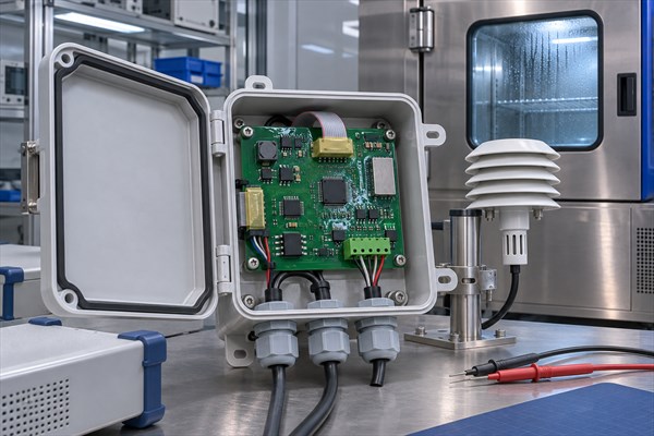
The appropriate protection depends on the actual installation environment.
- High Humidity and Condensation: Use suitable conformal coating, cleanliness controls, and enclosure protection. Moisture and surface contamination can create leakage paths and promote corrosion.
- Corrosive Environments: Protect exposed contacts and select compatible connectors and coating materials. Equipment installed near wastewater, industrial chemicals, or corrosive gases may require additional protection.
- Selective Conformal Coating: Mask sensor openings, connectors, and specified electrical contacts. Humidity and gas sensors must retain access to the measured environment, and coating materials must not enter their sensing cavities.
- Temperature Cycling: Check component temperature ratings, solder-joint quality, mechanical support, and material compatibility. Repeated thermal expansion and contraction can stress connections and solder joints.
- Outdoor Installation: Combine PCB-level protection with appropriate enclosure sealing, cable interfaces, and condensation management. Conformal coating alone does not make an assembly waterproof.
For products requiring demonstrated environmental reliability, temperature cycling, humidity exposure, or other qualification tests should be defined in the project specifications.
What Environmental Monitoring PCB Manufacturing and Assembly Services Does EBest Circuit Offer?
EBest Circuit provides custom PCB fabrication, component sourcing, SMT/THT assembly, inspection, and functional testing for environmental monitoring electronics.
Our manufacturing services include:
PCB Fabrication
- Single-sided, double-sided, and multilayer FR-4 PCB manufacturing.
- HDI, flexible, and rigid-flex PCB manufacturing when required.
- Custom PCB thickness, copper weight, stackup, and surface finish.
- Bare PCB electrical testing and dimensional inspection.
- Prototype, small-batch, and mass-production manufacturing.
PCB Assembly
- SMT assembly of sensor ICs, microcontrollers, analog front-end components, and wireless modules.
- Through-hole assembly of connectors, terminals, and other leaded components.
- Double-sided SMT and mixed-technology assembly.
- Turnkey and customer-supplied component assembly.
- Firmware programming and functional testing according to agreed requirements.
Manufacturing Review
Before production, EBest Circuit reviews the supplied Gerber files, BOM, and assembly documents.
For environmental monitoring PCBs, particular attention is given to:
- Sensor soldering profiles and cleaning restrictions.
- Component package and placement compatibility.
- Conformal coating and masking requirements, where specified.
- Approved component substitutions.
- Required inspection and functional testing procedures.
These checks help identify manufacturing conflicts before production while keeping the customer’s approved electrical design and component specifications unchanged.
How Are Environmental Monitoring PCB Assemblies Inspected and Tested?
Environmental monitoring PCB testing must verify both manufacturing quality and specified electrical functions. A PCB that passes visual inspection may still have unstable power, incorrect sensor connections, or measurement-channel faults.
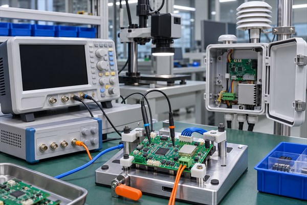
EBest Circuit supports the following inspection and testing methods according to project requirements:
- Bare PCB Electrical Testing: Checks for open and short circuits before component assembly.
- SPI: Verifies solder paste deposition before SMT component placement.
- AOI: Identifies visible component placement, polarity, and soldering defects.
- X-Ray Inspection: Examines applicable hidden solder joints, including BGA connections, when required.
- Functional Testing: Checks specified power supplies, sensor interfaces, communication functions, and circuit responses.
For environmental monitoring PCB assemblies, functional testing may include:
- Measuring regulated voltage and current consumption.
- Verifying I²C, SPI, UART, or other specified sensor interfaces.
- Applying known electrical signals to analog measurement channels.
- Checking firmware programming and configuration.
- Verifying wireless communication functions under defined conditions.
For example, an analog water-monitoring interface can be tested using an appropriate reference signal to confirm its electrical response.
However, this does not establish the accuracy of the complete water-quality instrument.
Sensor calibration and system-level environmental qualification require separate test procedures and acceptance criteria. The required inspection and testing scope should be confirmed before production.
What Is the Lead Time for Environmental Monitoring PCB Manufacturing and Assembly?
Environmental monitoring PCB manufacturing lead time depends on layer count, PCB specifications, component availability, and testing requirements.
EBest Circuit’s published standard lead time references are:
- 2-Layer FR-4 PCB: 8 days.
- 4-Layer FR-4 PCB: 10 days.
- 6-Layer FR-4 PCB: 10 days.
- PCBA Assembly: Approximately 1 week as a separate assembly-service reference.
These standard PCB manufacturing lead times apply to FR-4 prototype boards with a total board area below 1 m², under the following conditions:
- Board Thickness: 0.4–1.6 mm.
- Copper Weight: H/H or 1 oz.
- Surface Finish: Lead-free HASL.
- Solder Mask: Green.
- Silkscreen: White.
- Minimum Trace Width/Spacing: Greater than 8 mil.
- Minimum Hole Size: Greater than 0.3 mm.
- Minimum Annular Ring: Greater than 10 mil.
Special requirements such as ENIG, HDI structures, fine-line fabrication, selective conformal coating, or additional testing may change the manufacturing schedule.
For turnkey PCBA orders, sensor and wireless module availability must also be considered. Specialized components may require additional procurement time.
The published one-week PCBA lead time is a separate assembly reference, not a guaranteed total turnkey manufacturing schedule.
The final lead time is confirmed after reviewing the PCB files, BOM, order quantity, material availability, and testing requirements. International shipping time is additional.
How Much Does Environmental Monitoring PCB Manufacturing and Assembly Cost?
Environmental monitoring PCB manufacturing cost depends on PCB construction, sensor components, assembly complexity, production quantity, and testing requirements.
The main cost factors are:
- PCB Structure: Standard 2-layer FR-4 boards generally cost less to fabricate than comparable multilayer or HDI PCBs. Additional layers should be justified by routing and electrical requirements.
- Component Selection: Gas sensors, pressure sensors, precision analog components, and wireless modules may account for a significant portion of the BOM. Availability and approved alternatives also affect quotation.
- Assembly Complexity: Fine-pitch components, double-sided SMT, through-hole connectors, and restricted cleaning procedures require different manufacturing operations.
- Environmental Protection: Selective conformal coating, masking, curing, and additional inspection increase processing requirements.
- Testing and Quantity: Custom fixtures, firmware programming, and measurement verification add preparation work. Repeat production can distribute setup costs across more units.
To avoid unnecessary cost, confirm the PCB layer count, component availability, coating requirements, and testing scope before ordering.
For repeat production, stable BOM revisions and reusable test fixtures can also reduce avoidable manufacturing changes.
Why Choose EBest Circuit for Environmental Monitoring PCB Manufacturing and Assembly?
EBest Circuit helps environmental monitoring equipment manufacturers reduce supplier coordination, control assembly risks, and maintain consistent manufacturing requirements from prototype to production.
- One Manufacturing Partner: PCB fabrication, component sourcing, and assembly can be coordinated through EBest Circuit, reducing communication between multiple suppliers.
- Sensitive Sensor Handling: Component-specific soldering, cleaning, and protection requirements can be reviewed before assembly to help prevent avoidable sensor damage.
- Flexible Manufacturing: Support for standard FR-4, multilayer, HDI, and specialized PCB structures allows customers to manufacture different monitoring products according to approved specifications.
- Defined Quality Control: PCB electrical testing, SMT inspection, and agreed functional testing help identify manufacturing defects before shipment.
- Prototype-to-Production Support: Approved BOMs, fabrication files, and assembly instructions provide a consistent basis for repeat manufacturing.
EBest Circuit’s published quality management certifications include ISO 9001, ISO 13485, IATF 16949, and AS9100D. Customers with specific certification requirements can request the applicable certificate and scope for review.
Environmental Monitoring PCB Manufacturing and Assembly Case Study
Project Background
EBest Circuit has reported supplying PCBA assemblies to a Swiss IoT monitoring solutions provider for smart-building and energy-management applications.
The customer’s projects include flat-roof monitoring and HVAC filter monitoring, both requiring environmental sensing and remote communication.
Project Requirements and Challenges
The flat-roof monitoring application uses temperature, humidity, and water-leak detection to monitor conditions within roof structures.
The HVAC filter-monitoring application collects pressure differential, temperature, and humidity data to support maintenance decisions.
These applications require reliable sensor connections, power management, wireless communication, and PCB assemblies suited to their installation environments.
EBest Circuit Manufacturing Support
EBest Circuit supplied PCBA assemblies for the customer’s monitoring applications.
The published project description identifies LoRa communication and sensor-based monitoring functions. The manufacturing scope included supplying assembled electronic boards for the customer’s monitoring systems.
Project Results
According to EBest Circuit’s published project account, the supplied PCBA assemblies have been used in building-monitoring applications across Europe.
These systems support remote monitoring and maintenance notifications based on collected sensor data.
Specific PCB layer counts, production quantities, inspection results, and independently verified performance improvements have not been publicly disclosed.
FAQs About Environmental Monitoring PCB Manufacturing and Assembly
Q1: Can EBest Circuit assemble PCBs using customer-supplied environmental sensors?
A1: Yes. Customer-supplied sensors can be used for consigned assembly. Provide exact part numbers, quantities, packaging details, and handling instructions.
Q2: Can multiple environmental sensors be connected to one PCB?
A2: Yes. A single PCB can support compatible analog and digital sensors when the approved design accommodates their electrical and mechanical requirements.
Q3: Can LoRa or NB-IoT modules be assembled on environmental monitoring PCBs?
A3: Yes. These modules can be assembled according to the approved BOM and PCB layout. Antenna performance and regulatory compliance require appropriate system-level verification.
Q4: What happens if a specified environmental sensor is out of stock?
A4: Component availability is reviewed during sourcing. Any proposed substitute affecting the approved specification must receive customer approval before use.
Q5: Can environmental monitoring PCBA be supplied without external sensor probes?
A5: Yes. PCB assemblies and external probes can be supplied separately when permitted by the approved product configuration.
Q6: Can firmware be programmed before shipment?
A6: Yes, when included in the agreed assembly service. Customers should provide the approved firmware, programming instructions, and verification requirements.
Q7: Can different PCB revisions be produced in one order?
A7: Yes, subject to manufacturing review. Each revision requires separate approved fabrication files, BOM, and assembly identification.
Q8: Which IPC acceptance class should environmental monitoring PCBA follow?
A8: The appropriate IPC-A-610 class depends on the product’s reliability and contractual requirements. Customers should specify the required class and revision before production.
Q9: How should assembled sensor PCBs be packaged for shipment?
A9: Use ESD-safe and mechanically protective packaging compatible with the sensors. Exposed sensing elements may require additional contamination protection.
Q10: What information is required for an environmental monitoring PCB quotation?
A10: Provide Gerber or ODB++ files, PCB specifications, BOM, pick-and-place data, assembly drawings, order quantity, required component date codes, delivery location, and target delivery date. Include any special coating, programming, or testing requirements.
Reliable environmental monitoring equipment depends on PCB manufacturing and assembly processes that preserve sensor functionality, signal integrity, and environmental protection.
EBest Circuit provides custom environmental monitoring PCB manufacturing and assembly services, supporting prototypes, small batches, and mass production. Send your PCB files, BOM, order quantity, delivery requirements, and testing specifications to sales@bestpcbs.com for manufacturing review and quotation.