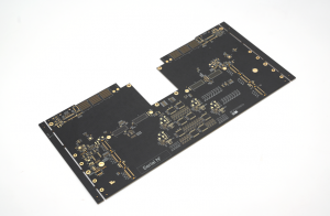
A trace can look continuous in CAD while the copper that carries its return current is interrupted. If a fast signal crosses a gap in its reference plane, first look for a route over continuous copper. A return bridge is not a default fix, especially if the gap provides safety isolation.
What Current Is Returning?
A driver and receiver are part of a current loop. At high frequencies, nearby reference copper helps provide a low-inductance return path. Trace length alone describes only the outward part of the loop. The Texas Instruments high-speed layout guide discusses how reference-plane gaps interrupt that path.
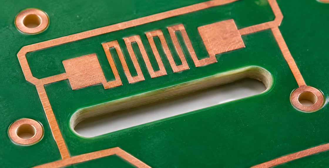
A Physical Slot Is Not the Only Interruption
A milled opening removes board material. A copper void removes reference metal without necessarily cutting the substrate. A row of overlapping antipads can also interrupt copper. Inspect the actual reference layer rather than assuming that only visible board cutouts matter.
Detailed Layout Parameters to Record
| Input | Unit or record | Why it matters |
| — | — | — |
| Signal and reference layers | Layer IDs | Identifies the intended return |
| Void location and width | X/Y and mm | Locates the interruption |
| Trace-to-reference spacing | mm | Helps evaluate field coupling |
| Edge rate | Time and definition | Informs relevant frequency content |
| Reference connection | Net, via and location | Defines the intended return transfer |
Reroute vs Change Layers vs Bridge
| Option | Use when | Verify |
| — | — | — |
| Reroute on the same layer | Continuous reference exists nearby | Entire new path and timing |
| Change signal layers | New reference is viable | Return transfer and via geometry |
| Approved AC bridge | Circuit permits the two regions to couple | Component parasitics and actual response |
Trace the Reference From Source to Receiver
Overlay the signal and its reference copper. Follow each segment, bend and transition. Name the reference after each layer change; the same net name on two layers does not identify the physical path between them. Use the BestPCBs ground-plane guide for the wider layout review.
Worked Example: A Clock Crossing a Connector Void
Suppose a clock trace on L1 references L2 but crosses a copper keepout under a connector. One revision adds 8 mm of trace to route around the void over continuous L2. Compare its timing and signal integrity with the short crossing. The added length is an example, not a rule that longer routing always wins.
Check a Differential Pair as a Real Pair
A differential pair still interacts with reference copper. Geometry changes or imbalance can disturb the pair and contribute to mode conversion. Review both traces and the corresponding plane region. Do not assume that a pair is exempt just because its signals are complementary.
A Stitching Via Cannot Bridge Every Gap
A nearby return via can help connect same-net reference planes at a layer transition. It cannot connect two regions unless there is a legitimate conductive path between them. Confirm the net and layer connections before adding a via that looks useful only in plan view.
Keep Intentional Isolation Intact
Do not bridge a safety or functional isolation gap as a layout cleanup. An inter-domain signal may require an isolator or another approved architecture. Treat any proposed change across the barrier as a separate engineering decision with its applicable clearances and requirements.
Look for a Discontinuity in the Right Test
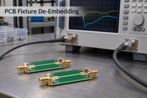
An impedance plot can help locate a reflection, while eye or emissions testing addresses different system outcomes. Where possible, compare two otherwise similar layouts to see what the routing change does. A standard coupon that lacks the gap will not validate that local crossing.
Recheck the Manufacturing Output
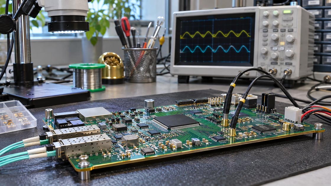
A plane shape can change after copper repour, keepout edits or layer export. Review the released copper artwork with the routed signal, especially at connector pin fields and plane boundaries. Record the layer pair, affected net and evidence for any accepted exception.
Decide What to Change First
Start by restoring a continuous reference without touching isolation or power architecture. If that is not possible, compare an alternate layer and an approved reference transfer. Use the interface’s performance targets to decide whether further simulation or hardware validation is warranted.
Request a Stackup Review
Share the affected layer pair, connector layout and net requirements with Best Technology.
FAQ
Is a trace over a small gap always a problem?
The impact depends on the gap geometry, trace-to-plane spacing, edge rate and the return paths available nearby. Do not assume the effect is negligible because the gap looks small at board scale. Compare the actual stackup and verify the relevant channel or emissions requirement if necessary.
Is clock frequency the same as edge rate?
No. Frequency describes how often the clock repeats, while edge rate describes how quickly it changes level. A low repetition-rate signal can still have fast edges. Review the driver’s transition behaviour and interconnect geometry when deciding whether the crossing needs high-frequency attention.
Can a capacitor fix every plane split?
No. A capacitor may provide an AC path in a design that permits it, but connection inductance, placement, frequency and safety constraints matter. Do not use it to bypass an isolation requirement. Prefer a route over continuous reference copper when it meets the design goals.
Do I need a ground via every time the signal changes layers?
Review whether the signal’s reference changes and where the corresponding return current can transfer. A nearby same-net connection can be useful when two reference planes are involved. A via is not a substitute for identifying the reference layers, and unrelated reference nets must not be shorted.
Can I route around the slot if the trace gets longer?
Often that is a useful option to compare, but validate both delay and routing constraints. Estimate the additional path length, check pair matching or timing where relevant, and review the entire return path. Do not judge either option on trace length alone.
Does a ground pour on the trace layer fix the issue?
Only if the resulting geometry and connections provide a suitable reference for that specific route. Isolated or weakly connected copper is not automatically a good return path. Check the copper spacing, grounding and stackup, and use an appropriate model when the behaviour is important.
Will an impedance coupon show a slot crossing?
Only if it intentionally represents the relevant structure. A straight coupon on uninterrupted reference copper can characterize the ordinary trace but not a local return interruption under a connector. Check what the coupon represents and use a targeted structure or board measurement if the crossing must be validated.
Should I merge two separate grounds to avoid the gap?
Do not merge domains simply to make a routing overlay look cleaner. First establish why they are separated and what signal must cross. Follow the system’s safety and circuit requirements, and consider rerouting or an approved interface architecture before modifying the intended isolation boundary.