





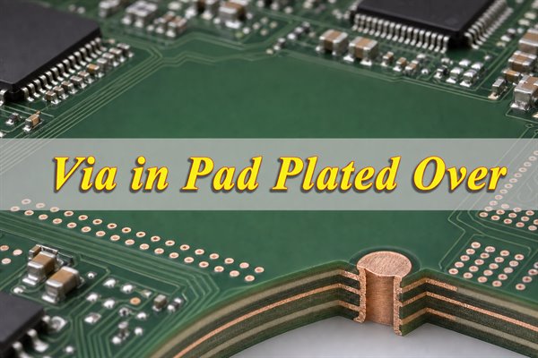
Via in pad plated over (VIPPO) places a filled, planarized and copper-capped via directly in a component land. It can free routing space under fine-pitch packages and create a solderable pad, but only when the fill, cap, surface flatness and fabrication notes are controlled as one manufacturing requirement.
The key question is whether the structure can be fabricated repeatedly without drawing solder from the joint or creating an uneven mounting surface. The quotation must cover filling, planarization, cap plating and inspection—not a vague request for “via in pad.”
What Is Via in Pad Plated Over (VIPPO)?
VIPPO is a complete via-protection structure, not simply a via located inside a pad. The hole is plated, filled, cured, planarized and plated over with copper so the finished land can receive solder paste and a component termination.
The barrel provides the electrical connection; the fill closes and supports the cavity. Planarization removes excess fill, and the copper cap restores a continuous solderable land. Without that closure, an open in-pad via can pull solder into the hole during reflow and contribute to solder starvation, component tilt or inconsistent joints.
How Does Via in Pad Plated Over Differ from Via-in-Pad and POFV?
Via-in-pad identifies where a via is placed; VIPPO and POFV identify how a filled via is finished. The terms overlap, but they are not interchangeable in every context. A via can sit inside a component pad without being filled or plated over, while a POFV structure does not have to be located in a component pad.
| Terminology | Definition | Construction Requirements | Direct Component Soldering | Engineering Distinction |
| Via-in-Pad | Via location: the via is placed within a component land | May be open, tented, filled, covered or copper capped | Only when the selected treatment creates a flat, solderable land | It is a layout concept, not a complete fabrication specification. An open in-pad via can wick solder during reflow. |
| VIPPO | Via-in-pad plated over | The in-pad via is plated, filled, cured, planarized and copper capped | Yes, when the cap, flatness and final finish meet the approved requirements | VIPPO converts the in-pad via opening into a continuous component land and helps prevent solder loss into the hole. |
| POFV | Plated over filled via | The via is filled, planarized and plated over; its location depends on the design | Yes, if it forms an approved component land; otherwise it may serve another structural purpose | POFV is the broader process term. When the plated-over filled via is located inside a component pad, it is commonly treated as VIPPO. |
Specify Via-in-Pad for placement, VIPPO when the via becomes part of a solderable component land, and POFV for the broader filled-and-plated-over process. VIPPO and POFV are commonly associated with IPC Type VII filled-and-capped via terminology, but the drawing must still identify the holes, fill, cap, surface finish, inspection criteria and applicable document revision.
When Should You Use VIPPO Instead of Dog-Bone Fanout?
Choose VIPPO only when it solves a verified routing, electrical, thermal or package-interface problem that dog-bone fanout cannot solve efficiently. Dog-bone fanout remains the lower-risk choice when an adjacent via and short surface trace fit within the routing rules and meet performance targets.

- No escape space: Fine-pitch BGA, LGA and other dense bottom-terminated packages may leave no room for a trace neck and adjacent dog-bone via. Placing the via inside the land preserves the escape channel and can make inner pad rows routable.
- Layer-count pressure: Direct vertical transitions can simplify breakout and may reduce escape layers or avoid extremely narrow traces and clearances. Compare the complete stackup cost because fewer layers may not offset the fill-and-cap process.
- Short electrical path: Removing the dog-bone trace can reduce connection length, loop area and transition inductance for selected high-speed signals or power-decoupling paths. Confirm the benefit through channel or power-integrity analysis; a shorter visible trace does not guarantee better system performance.
- Direct thermal path: A via array beneath a QFN, power device or exposed thermal pad can connect the land to internal planes or opposite-side copper. Evaluate via count, copper distribution, fill and stencil segmentation together to avoid paste loss or uneven package seating.
- Solderable in-pad surface: Filling, planarization and copper capping restore a continuous pad for paste printing and component placement. An open, tented or resin-covered via is not equivalent when a component terminal sits over the opening.
- Dog-bone fits: Keep the adjacent via when it meets routing and electrical requirements. It is easier to fabricate, inspect, probe and rework, and it separates via tolerances from the component land.
- Prototype access: Debug builds benefit from accessible traces and test points. When density permits, dog-bone fanout makes trace cutting, pad repair and component rework easier.
- Compare total cost rather than the via surcharge alone: VIPPO adds filling, curing, planarization, copper capping and inspection, while dog-bone routing may require more board area, finer lines or additional layers. Compare both complete constructions at prototype and production quantities using the same electrical and inspection requirements.
- Confirm supply-chain capability before selecting VIPPO: The proposed via diameter, layer span, aspect ratio, fill material, cap structure, flatness and inspection plan must fit the fabricator’s qualified process. A layout is not ready simply because the CAD tool permits a via inside the pad.
Make the VIPPO vs. dog-bone fanout decision during DFM, not after routing is complete. Select VIPPO only when its routing or performance benefit outweighs the added fabrication, inspection and rework burden.
How Does the Via in Pad Plated Over Process Work?
Via in pad plated over is a controlled build-up process: form and plate the via, fill its cavity, cure and planarize the fill, then plate copper across the opening to restore a flat component land. The production route changes with through vias, blind vias, microvias, sequential lamination and the fabricator’s qualified process, but the functional stages remain similar. These dependencies become especially important in HDI PCB fabrication, where sequential lamination and stacked or staggered microvias must be reviewed as one construction.
- Identify the designated vias: The fabrication data must show which holes require VIPPO, their finished size, layer span and associated component pads. This prevents ordinary vias from being filled unnecessarily and avoids ambiguity between through vias, blind vias and microvias.
- Form the holes: Through and mechanically drilled blind vias are drilled with controlled tool size and registration; laser-drilled microvias are formed to the specified capture and target layers. Hole position and geometry must support reliable plating and later planarization.
- Clean and prepare the hole walls: Debris and resin smear are removed, and the exposed dielectric is conditioned for metallization. Inadequate desmear can weaken the copper-to-dielectric interface or leave an unreliable electrical connection.
- Metallize and copper-plate the barrel: A conductive seed layer is established before electrolytic copper builds the via wall. Barrel continuity and copper distribution must be acceptable before filling because the fill cannot repair thin plating, voids or poor interconnection.
- Clean and fill the via: The cavity is prepared and filled with the approved conductive or non-conductive material under controlled pressure or vacuum. The process must limit trapped air, internal voids and incomplete fill, especially in small-diameter or high-aspect-ratio structures.
- Cure the fill material: The filled panel follows the material supplier’s qualified time-and-temperature profile. Complete cure stabilizes the plug for planarization and later thermal cycles; under-cure can cause recession, cracking, contamination or cap-plating defects.
- Planarize the surface: Excess fill is removed until the plugged via is level with the surrounding copper land. The operation must avoid a recessed plug, a raised bump, excessive copper removal or damage to nearby fine features because these conditions can affect solder-paste deposition and component coplanarity.
- Deposit and plate the copper cap: The planarized opening is prepared, metallized and copper plated to create a continuous land over the filled via. Cap adhesion, coverage and thickness must meet the drawing and applicable acceptance criteria; filling alone does not create a VIPPO soldering surface.
- Complete the outer-layer features and finish: Imaging and etching define the final pad, after which solder mask and the specified surface finish are applied. The finished land must remain compatible with the selected BGA, QFN, LGA or other bottom-terminated component assembly process.
- Inspect and release the structure: Visual and dimensional checks assess pad flatness, surface defects and registration, while microsection or other agreed methods evaluate barrel copper, fill condition, cap continuity and internal interfaces. Sampling, acceptance limits and reporting should be defined before production rather than after a defect occurs.
A sound copper cap cannot compensate for poor hole-wall plating, trapped voids, incomplete cure or excessive planarization. Each stage must pass its own process control before the next operation begins.
Should VIPPO Vias Use Conductive or Non-Conductive Fill?
Non-conductive epoxy is a common choice because the plated barrel and copper cap carry the electrical current. Conductive fill may be considered for a specific thermal or electrical objective, but it should not be specified automatically.
| Decision factor | Non-conductive fill | Conductive fill |
| Electrical path | Current remains in the plated barrel and cap | Fill may contribute, but performance depends on material and interfaces |
| Thermal objective | Suitable when the copper structure provides the required path | Consider only when thermal analysis supports the benefit |
| Process control | Well suited to filling and planarization when matched to the via geometry | Material handling, cure behavior and plating compatibility require confirmation |
| Cost | Usually the more economical option | Typically carries a material and process premium |
The broader PCB via filling decision must also account for board thickness, finished via diameter, aspect ratio, via span, pad construction and reliability target. Approve the fill only after those variables have been reviewed; a material label alone is not a complete specification.
What Via in Pad Plated Over Design Rules Must Be Confirmed Before Layout Release?
The critical VIPPO PCB design rules must be agreed with the fabricator before the footprint and fanout are frozen. Generic capability values may not apply to the selected layer span, laminate, copper weight, via type or reliability class.
- Via type and layer span: Identify whether each feature is a through via, mechanically drilled blind or buried via, or laser-drilled microvia, and state its start and stop layers. These structures use different formation, plating and filling routes, so one rule cannot be applied to all of them.
- Drill size and finished hole size: Distinguish the tool or laser diameter from the finished plated opening. Confirm the tolerance and whether the drawing refers to the drilled, plated or final filled condition; mixing these definitions can invalidate aspect-ratio and plating reviews.
- Pad, capture land and annular ring: Check the component manufacturer’s land pattern, drill-to-pad registration allowance, required annular ring and area available for the copper cap. The design must retain a usable solderable land after fabrication tolerances, planarization and etching are considered.
- Aspect ratio and plating access: Review hole depth relative to diameter for each via family and confirm that chemistry can circulate through the structure. Deep or narrow vias are harder to metallize and fill consistently; blind, buried and through vias should therefore be reviewed separately.
- Microvia stacking and staggering: Define whether microvias are staggered, stacked or placed over a buried via, and confirm the permitted build-up sequence. Stacked structures concentrate stress and depend on the underlying fill and cap, so they may require additional process qualification and inspection.
- Fill material and filling scope: Specify conductive or non-conductive fill only when the electrical or thermal design requires it, and identify exactly which vias are included. Also confirm material compatibility with lamination, cure temperature, surface finish and assembly thermal cycles.
- Copper cap and surface condition: Define which side or sides require plating over, the required cap construction and the acceptance basis for continuity, adhesion and surface condition. Filling and tenting alone do not create a flat, solderable VIPPO land.
- Pad flatness and finished height: Agree how recess, protrusion and coplanarity will be measured and accepted. A recessed pad can disturb paste transfer, while a raised pad can prevent a BGA, LGA or QFN from seating evenly on adjacent lands.
- Solder mask and surface finish: Coordinate solder-mask-defined or non-solder-mask-defined lands, mask clearance and final finish with the footprint and assembly process. Confirm that mask registration and finish thickness will not reduce the intended solderable area or create uneven pad height.
- Electrical, thermal and assembly performance: Include high-speed via transitions and stubs in the channel model, and evaluate the complete copper-and-dielectric heat path for thermal pads. Then review stencil aperture, paste volume, package warpage, component coplanarity and reflow profile; conductive fill should not be treated as an automatic solution to signal, heat or solder-joint problems.
Do not release the layout until the fabricator has reviewed the proposed stackup, via table and representative component escape. Record the approved values in the controlled fabrication drawing or design rules rather than leaving them in email. Any change to laminate, copper weight, layer span, via diameter, fill system, surface finish or component footprint should trigger a focused VIPPO review before the data is released again.
How Should VIPPO Be Called Out in the Fabrication Drawing and Data Package?
A complete VIPPO callout identifies exactly which vias are filled and capped and how acceptance will be determined. A note that says only “plug vias” is open to interpretation.
- Dedicated identification: Provide a separate drill layer, via table or unambiguous coordinate-based designation for VIPPO holes.
- Structure definition: State the via span, whether it is through, blind, buried or microvia, and which surface receives the cap.
- Material requirement: Specify conductive or non-conductive fill, or authorize the fabricator to propose a qualified material for approval.
- Process requirement: Require filling, curing, planarization and copper capping where a solderable land is needed.
- Acceptance basis: Cite the applicable drawing, IPC product class, standard revision and any project-specific microsection or surface criteria.
- Data consistency: Ensure Gerber/ODB++, NC drill, stackup, drawing and netlist describe the same revision.
A practical note may state: “Fill designated vias with approved non-conductive epoxy, cure, planarize and copper cap to form solderable lands; use IPC-4761 Type VII terminology where invoked; acceptance per the approved drawing and applicable product specification.” Add project-specific values only after engineering agreement.
What VIPPO Defects Cause Fill Voids, Surface Depressions or Soldering Problems?
Most VIPPO failures begin with incomplete filling, poor planarization, weak cap plating or an already-defective plated barrel. The visible soldering symptom may appear late even though the cause was introduced during bare-board fabrication.
- Fill voids: Trapped air, poor fill penetration or unsuitable geometry can leave cavities that reduce support and may affect later thermal cycling.
- Surface depression: Fill shrinkage or underfilling can leave a recessed pad that changes paste distribution and joint geometry.
- Raised surface: Excess fill or insufficient planarization can prevent a package from seating evenly.
- Cap discontinuity: Thin, porous or cracked cap copper can expose the fill or create a weak solderable surface.
- Barrel defect: Smear, plating voids or cracks remain electrical and reliability risks even when the top cap looks acceptable.
- Moisture or contamination: Inadequate cleaning, cure or storage control can contribute to blistering, delamination or assembly defects.
Solder wicking should trigger an investigation of the actual via construction and cap integrity; it is not normal behavior for a correctly produced VIPPO structure.
How Should Finished Via in Pad Plated Over Vias Be Inspected and Accepted?
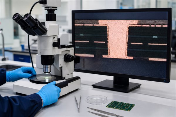
A complete via in pad plated over inspection plan combines surface inspection, dimensional checks, representative microsections and bare-board electrical testing. No single method verifies the soldering surface, copper cap, cured fill, plated barrel and electrical network.
- Confirm the acceptance basis: Before inspection, verify the released fabrication drawing, product class, applicable IPC document and revision, approved stackup, via map and any customer-specific requirements. The purchase package should define what is measured, the sampling plan, acceptance limits and required records; otherwise the supplier and customer may judge the same feature differently.
- Inspect the finished pad surface: Use appropriate lighting and magnification to check that the component land is continuous and clean. Reject or escalate exposed fill, open cap areas, pits, nodules, dents, scratches, contamination, lifted copper or damage that could interfere with solder-paste printing, wetting or component seating.
- Verify pad flatness and coplanarity: Measure the features specified on the drawing rather than relying on visual appearance. A recessed plug can reduce paste support, while a raised cap can hold a BGA, LGA or QFN terminal above adjacent lands. Measurement method, datum, sample quantity and allowable variation should be agreed before production.
- Check registration and finished geometry: Confirm that the plated-over area remains correctly located within the component land and that the final pad dimensions support the approved footprint. Misregistration, excessive planarization or over-etching can reduce the usable solderable area even when the via is electrically continuous.
- Review the copper cap: Cross-sectional evidence should show a continuous plated cap with no separation from the surrounding copper. Assess the cap thickness and coverage against the drawing and applicable acceptance criteria. A filled via without an acceptable copper cap is not an acceptable VIPPO soldering land.
- Evaluate the fill condition: On representative coupons or agreed production samples, examine fill completeness, internal voiding, recession, cracks and separation at the fill-to-barrel or fill-to-cap interfaces. The permitted condition must come from the governing specification and customer agreement because a generic void percentage does not describe every via geometry or reliability requirement.
- Examine the plated barrel and interconnect: Microsections should also assess hole-wall copper, internal-layer connections, corner condition and evidence of plating voids, cracks or separation. Good fill appearance cannot compensate for a weak conductive barrel or an unreliable connection to the target layer.
- Perform bare-board electrical testing: Test continuity and isolation using the approved netlist and test method. Electrical testing identifies opens, shorts and incorrect connectivity, but it cannot confirm pad flatness, cap adhesion, fill cure or all internal structural defects, so it must support rather than replace physical inspection.
- Use assembly validation when risk justifies it: For a new fine-pitch footprint, new VIPPO construction or high-reliability program, inspect first-article paste deposits, component seating and solder-joint consistency. X-ray or other assembly inspection may reveal solder loss, voiding or alignment problems, but the method and acceptance criteria should match the package and product requirements.
- Review lot records before release: Confirm the required certificate, electrical-test result, microsection images, dimensional report, material traceability and nonconformance history. Any out-of-limit result should be documented and dispositioned through the agreed deviation or corrective-action process, not accepted through an undocumented production judgment.
“Inspect to IPC” is not a complete acceptance instruction. The order should identify the document and revision, product class, designated VIPPO structures, cap and fill requirements, dimensional controls, sampling, records and rules for reporting nonconforming results.
How Does VIPPO Affect PCB Cost, Yield and Lead Time?
Via in pad plated over costs more than an open or simply covered via because it adds controlled operations and yield exposure. The premium depends on the number and geometry of filled vias, panel construction, material, inspection plan and production volume.
Cost drivers include selective or full-panel filling, cure cycles, planarization, additional copper processing, microsections and yield loss when flatness or fill quality fails. Conductive fill normally adds further material and qualification cost.
VIPPO can extend lead time because filling, curing, planarization, cap plating and, when required, microsection review are sequential operations. Material approval, unclear via classifications, or failed fill and flatness checks can add engineering holds, reprocessing or remake time. Confirm the approved construction and inspection plan before order release to reduce avoidable schedule delays.
Compare quotations against the same technical package. A low quote may exclude cap plating, treat VIPPO as ordinary plugged vias or omit required quality records.
What Should You Send for a VIPPO DFM Review and Quote?
Send one revision-controlled package that connects the component land, via structure, stackup, fabrication note and acceptance requirement. This allows engineering to review manufacturability before pricing is finalized.
- PCB production data: Gerber or ODB++, NC drill files, netlist and a clear revision identifier.
- Stackup: Layer count, materials, finished thickness, copper requirements and controlled-impedance information.
- VIPPO map: Designated via locations, via span, finished hole requirement, fill choice and cap side.
- Fabrication drawing: Applicable standard, product class, surface finish, inspection criteria and required quality records.
- Assembly context: BOM, assembly drawing, centroid data and relevant BGA/QFN package information when assembly is included.
- Commercial inputs: Prototype and production quantities, delivery target and expected approval stages.
EBest Circuit will confirm final VIPPO capability against the submitted stackup and via construction. Do not release the layout based on a generic capability value.
FAQs About Via in Pad Plated Over
Q1: Is an open via-in-pad acceptable for a hand-soldered prototype?
A1: It may be workable only when the joint is visible and additional solder can be applied. The result is process-dependent. For hidden BGA joints, fine-pitch parts or a design intended for production reflow, do not use hand-solder success as proof of production reliability.
Q2: Can I plug a via with solder or epoxy myself instead of ordering VIPPO?
A2: A manual plug may help a one-off experiment, but it is not equivalent to production VIPPO. It does not reproduce controlled hole filling, cure, planarization and copper capping and may trap flux or air, remain uneven or remelt during assembly. Therefore, do not treat it as a production substitute.
Q3: Does VIPPO make BGA or small-component rework more difficult?
A3: Yes, VIPPO can make component rework more difficult. The short direct connection to internal copper may increase local heat demand, and a pad integrated with a via is harder to isolate or repair if damaged. Establish the rework profile, board support and inspection method before attempting high-value BGA removal or replacement.
Q4: Can a VIPPO land replace a dedicated test point?
A4: No—do not assume a VIPPO land can replace a dedicated test point. A land under a component is inaccessible after assembly, while an exposed plated-over via may not have the probe area, spacing or durability needed for repeated contact. Preserve dedicated test access for programming, ICT and troubleshooting unless the test engineer approves another method.
Q5: Can VIPPO under one pad of a small passive cause tombstoning?
A5: Yes, tombstoning can still occur despite using VIPPO. VIPPO prevents an open hole from draining solder, but the two terminations may still heat or wet unevenly. Compare copper balance, plane connections, paste volume and pad geometry on both ends because a capped via does not eliminate thermal imbalance.
Q6: Will VIPPO stop potting compound or conformal coating from passing through a via?
A6: A properly filled and copper-capped via closes that specific leakage path. Coating or potting qualification must still consider board edges, connectors, other holes, material adhesion and thermal expansion because VIPPO addresses only the designated via opening.
Q7: Does VIPPO eliminate the need for X-ray inspection under a BGA?
A7: No, VIPPO does not eliminate the need for BGA X-ray inspection. It removes the open via cavity from the land, but hidden solder joints can still have insufficient solder, bridging, voiding or alignment defects. Use an inspection plan matched to the package, process risk and acceptance requirements.
Q8: Can a defective VIPPO copper cap be repaired after final surface finishing?
A8: A defective copper cap should not be repaired without formal engineering approval. Local rework may not restore the original cap interface, flatness, finish or reliability. Do not accept a cosmetic touch-up as an equivalent repair without an approved procedure and inspection evidence.
Q9: Can components be mounted on opposite sides over the same filled and plated via?
A9: Double-sided component placement may be feasible when both surfaces are intentionally capped. The nets, pad geometries and assembly sequence must also be compatible. Confirm side-specific flatness, finish, paste printing and reflow constraints because double-sided placement is both a fabrication and assembly decision.
Q10: Should a prototype and its production version use the same via treatment?
A10: Use the production VIPPO construction when the prototype must validate assembly yield or reliability. A simplified open or tented via may reduce prototype cost, but it changes paste behavior and can hide production risks. Document every prototype deviation before interpreting the results.
Send your design for a VIPPO DFM review before order release. Email the Gerber or ODB++ files, stackup, via table, BOM, quantities and assembly requirements to sales@bestpcbs.com. Include the delivery target and any impedance, surface-finish, inspection, programming or functional-test requirements. We will review the via construction, identify manufacturing risks and prepare a production quotation.
You may also like



Tags: via in pad design rules, Via in Pad Inspection, Via in Pad Plated Over, Via in Pad vs Dog-Bone Fanout