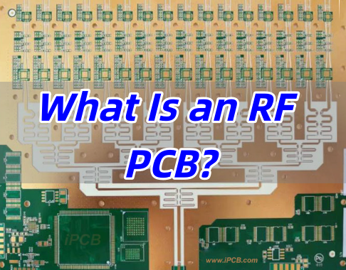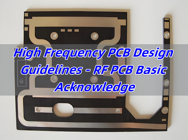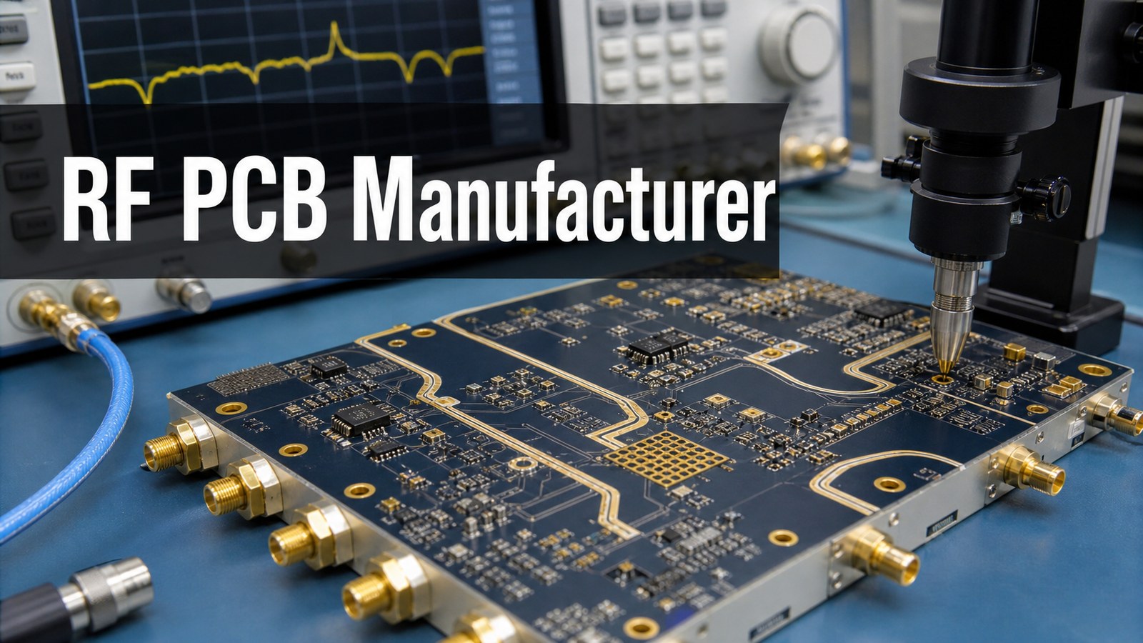
An RF PCB manufacturer builds circuit boards for radio-frequency and microwave signals where laminate choice, controlled impedance, copper geometry, surface finish and test planning affect signal loss and repeatability. For buyers, the practical question is whether the supplier can review material, stackup, transmission-line geometry, connector launch, impedance targets and RFQ files before fabrication.
This guide focuses on commercial RF, wireless, telecom, sensor and high-frequency electronics projects. Specific capability references come from Best Technology / bestpcbs process records where the data is available, and project-specific compliance requirements should be confirmed before quotation.
RF PCB Manufacturer at a Glance
A reliable RF PCB manufacturer should treat the board as part of the signal path, not only as a carrier for components. Small changes in laminate, dielectric thickness, copper roughness, trace width, solder mask and connector launch can change RF performance.
| RF decision area | What to confirm | Why it matters |
|---|---|---|
| Material | Rogers, Taconic, PTFE, high-Tg FR4 or hybrid stackup | Controls dielectric constant, loss and availability. |
| Impedance | Target value, tolerance, trace type and reference plane | Reduces reflection and mismatch. |
| Stackup | Layer count, dielectric thickness, copper weight and mixed materials | Controls repeatability and manufacturability. |
| RF details | Connector launch, via fence, grounding, transition and keepout rules | Prevents avoidable RF loss or instability. |
Is Your RF PCB Project at Risk From Material or Impedance Assumptions?
RF PCB buyers need a supplier that treats the board as a signal-performance project, not just a standard fabrication order.
| Customer Pain Point | Project Risk | How bestpcbs Helps |
|---|---|---|
| RF material is selected without application context | Loss, stability or cost may not match the frequency range | bestpcbs asks for frequency range, material notes and performance requirements before confirming the quote path. |
| Controlled impedance targets are not supplied | The board can be fabricated but still miss RF behavior expectations | bestpcbs reviews stackup, copper, trace notes and impedance requirements before production. |
| Via transitions and grounding are not reviewed | Small layout details can affect RF performance and repeatability | bestpcbs checks drill data, RF layout notes, grounding approach and special requirements during DFM review. |
| Testing requirements are left open | The buyer may not know what has been verified before shipment | bestpcbs confirms electrical, impedance or customer-defined test expectations in the RFQ stage. |
RF PCB Supplier Checks Before Quoting
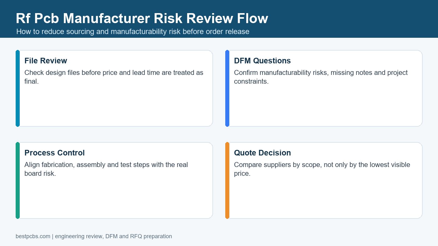
RF PCB sourcing should start with material, stackup, impedance and test requirements, not only with board size and quantity. Small assumptions about dielectric material, copper roughness, via transitions or ground return paths can change RF behavior.
Ask the supplier to review frequency range, material notes, controlled impedance targets, stackup drawings, plated holes, surface finish and testing expectations before production. This helps reduce surprises when a prototype moves toward repeat manufacturing.
RF PCB Capabilities Buyers Should Verify
Before selecting an RF PCB manufacturer, verify material availability, line/space capability, surface finish, board thickness range, impedance needs and test expectations. RF capability depends on the exact frequency range, laminate and layout, so a generic claim is not enough.
| Capability item | Verified bestpcbs reference | RFQ note |
|---|---|---|
| High-frequency materials | Rogers 4003 / 4350 / 5880, Taconic laminates, PTFE, Nelco and other special materials are listed in the capability record. | Confirm availability and substitutions before quote release. |
| Layer count | FR4 normal range 1-10 layers, special range 10-32 layers in the referenced PCB capability sheet. | Hybrid RF stackups require separate confirmation. |
| Fine lines | 1/2 oz inner layer 4/4 mil normal and 3/3 mil special; 1/1 oz outer layer 4/4 mil normal and 3/3 mil special. | Check line width against impedance, copper and finished plating. |
| Surface finish | OSP, HASL, ENIG, immersion silver, immersion tin, ENEPIG and hard-gold-related options are listed with conditions. | Choose finish based on assembly, RF pads and connector needs. |
RF Materials and Laminate Selection
RF material selection should be driven by dielectric constant, loss tangent, thickness control, copper surface, frequency range, availability and cost. Using a familiar laminate name without checking stackup and supplier availability can create quote delays.
Bestpcbs records list high-frequency material options such as Rogers 4003 / 4350 / 5880, Taconic laminates, PTFE and related high-performance materials. The RF Board manufacturer page and RF PCB product page are useful internal references for the service scope.
Controlled Impedance and Transmission Lines
Controlled impedance should be specified before fabrication because RF traces depend on laminate thickness, copper weight, solder mask, trace geometry and reference plane continuity. The manufacturer should know whether the design uses microstrip, stripline, coplanar waveguide or another controlled structure.
Send target impedance, tolerance, frequency range, layer stackup and whether test coupons are required. For mixed digital and RF boards, also identify high-speed nets, RF nets and sensitive return paths. The impedance control PCB page is a relevant reference.
Connector Launch, Grounding and Via Fencing
Connector launch, grounding and via fencing often determine whether an RF PCB performs well after assembly. A board can use the correct laminate and still perform poorly if transitions, pads or ground stitching are not reviewed.
- Provide connector part numbers and recommended footprints.
- Mark RF keepout areas and critical transmission lines.
- Confirm via fence spacing and grounding expectations.
- Review transitions between connectors, antennas, filters, amplifiers and test points.
- State whether RF testing or only manufacturing inspection is required.
Hybrid RF Stackups
Hybrid RF stackups combine high-frequency laminates with FR4 or other materials, so they need a more careful manufacturing review than standard FR4 boards. Material expansion, lamination behavior and thickness control can affect repeatability.
For hybrid builds, send a controlled stackup and identify which layers carry RF signals. If the design combines RF, digital control, power and PCBA in one board, include assembly constraints as part of the RFQ. Related internal reading includes the HDI PCB manufacturer RFQ guide when the design also uses dense routing or microvias.
RF PCB Cost Drivers
RF PCB cost is driven by laminate choice, stackup complexity, impedance control, low-loss material procurement, connector requirements, surface finish, testing and panel utilization. A lower quote may simply exclude material or test assumptions.
| Cost driver | Why it changes cost | How to control it |
|---|---|---|
| Special laminate | High-frequency materials may have MOQ or longer procurement time. | Approve alternates early when possible. |
| Impedance control | Requires stackup calculation and sometimes coupons. | Provide target values and tolerance up front. |
| Connector launch | May need footprint review or assembly care. | Send connector datasheets and drawings. |
| Testing | RF validation is different from basic electrical test. | Define what the supplier must inspect or test. |
Prototype and Production RF PCB Orders
Prototype RF PCB orders should prove material, stackup and connector performance before scaling to production. Production orders need stronger material control, repeatable stackups and clear acceptance criteria.
For prototypes, focus on engineering feedback, impedance targets and connector launch checks. For production, define laminate alternates, revision control, inspection records, packaging and whether assembly is included. If PCBA is needed, connect the RF board quote with the PCBA and PCB assembly service.
How to Compare RF PCB Manufacturers
Compare RF PCB manufacturers by their material knowledge, impedance review process, RF layout questions and quote assumptions. A supplier that asks the right RF questions early is more useful than one that only returns the fastest price.
- Do they ask for frequency range, material and stackup?
- Can they support controlled impedance and RF coupons if required?
- Do they separate normal capability from special procurement cases?
- Do they review connector launches and sensitive transitions?
- Do they avoid unsupported promises about RF performance without test criteria?
RFQ File Checklist for RF PCB Projects
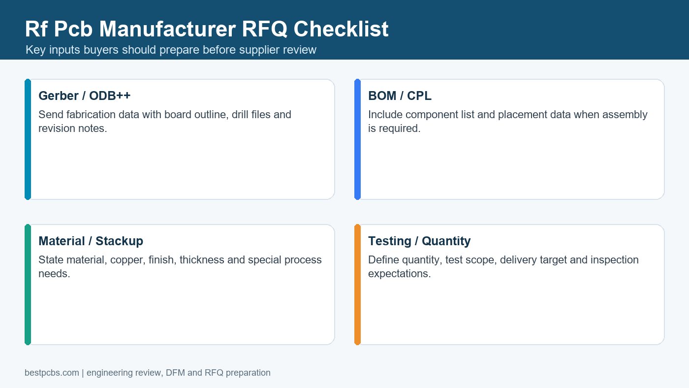
A complete RF PCB RFQ should include fabrication files, stackup, material, impedance targets, connector data, quantity, surface finish and test requirements. Without these inputs, the quote may not reflect the real RF design.
| RFQ item | Why it matters |
|---|---|
| Gerber or ODB++ | Defines copper, solder mask, drill, outline and manufacturing data. |
| Stackup | Defines dielectric thickness, laminate, copper and reference planes. |
| Impedance table | Lists RF nets, target values, tolerance and trace type. |
| Connector datasheets | Helps review launch geometry and assembly fit. |
| BOM, CPL and drawings | Required if the project includes assembly or turnkey PCBA. |
| Test requirements | Clarifies whether the supplier performs E-test, impedance, inspection or RF-related checks. |
Internal Resources for RF PCB Buyers
RF PCB buyers should connect RF material pages, impedance resources and manufacturing checklists before ordering. Useful internal references include the multilayer PCB manufacturing checklist, the PCB fabrication manufacturer guide, and the PCB assembly manufacturer RFQ checklist when components are part of the project.
Common RF PCB Sourcing Mistakes
Common RF PCB sourcing mistakes include quoting without stackup, changing laminates without impedance review, ignoring connector launch details, and treating all high-frequency suppliers as interchangeable. These mistakes can create performance problems after the board is already assembled.
- Do not approve laminate substitutions without checking impedance and loss needs.
- Do not leave connector launch and grounding details out of the RFQ.
- Do not compare quotes unless material, surface finish and testing assumptions match.
- Do not assume a basic electrical test proves RF performance.
- Do not use regulated project assumptions unless the supplier has confirmed the required scope and credentials.
Frequently Asked Questions About RF PCB Manufacturers
What does an RF PCB manufacturer do?
An RF PCB manufacturer fabricates circuit boards for radio-frequency and microwave signals, with attention to laminate choice, impedance, trace geometry, grounding and RF-related assembly constraints.
What materials are used for RF PCBs?
RF PCBs may use high-frequency laminates such as Rogers, Taconic, PTFE-based materials, high-Tg FR4 or hybrid material stackups, depending on frequency, loss target and cost.
Is controlled impedance required for RF PCBs?
Usually yes for defined RF transmission lines. The RFQ should include target impedance, tolerance, stackup and trace type so the manufacturer can review feasibility.
Can RF PCBs also include assembly?
Yes, if the supplier supports PCBA. Assembly planning should include RF connectors, shield parts, sensitive components, test access and handling requirements.
Final RFQ Recommendation
Choose an RF PCB manufacturer that reviews material, stackup, impedance, connector launch, grounding and test expectations before quoting. A precise RFQ is the best way to avoid late material changes and signal-integrity surprises.
For an RF PCB quotation, send your Gerber or ODB++ files, stackup, laminate preference, impedance table, connector datasheets, quantity, surface finish, BOM, CPL, assembly drawings if needed, test requirements and target lead time to sales@bestpcbs.com. The Best Technology / bestpcbs team can review the package and identify which RF manufacturing assumptions need confirmation before prototype, pilot or production release.