





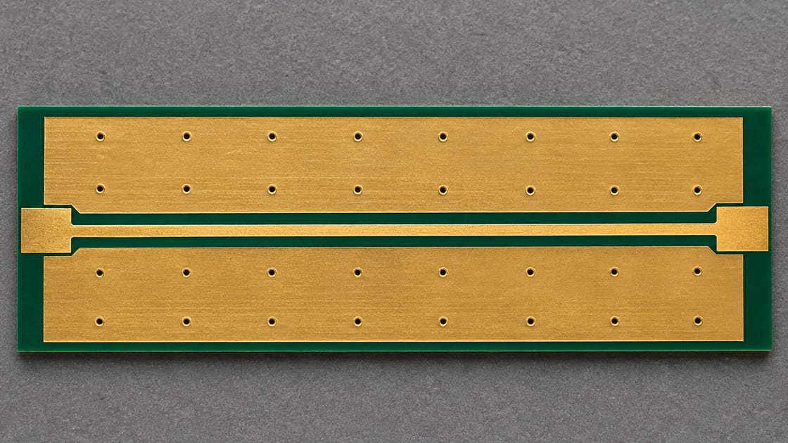
Conventional coplanar waveguide (CPW) has a signal conductor between two same-layer ground conductors without a metal plane beneath the substrate. Grounded CPW (GCPW), also called conductor-backed CPW, adds a lower ground plane electrically connected to the side grounds. The same top-layer width and gap do not make these two structures electrically equivalent.
In a teaching example, a designer calculates a 50-ohm antenna feed, then adds bottom copper and stitching vias to the board. The trace has not changed on screen, but the cross-section has. This guide explains how to select a model that represents the board, rather than assuming that any calculator labeled “coplanar” will do.
Identify the Cross-Section Before Naming the Line
Start with where copper exists above, beside and below the signal, not the label attached to a CAD rule. Sonnet’s CPW documentation distinguishes conventional, grounded and floating structures. In its definitions, lower copper that is not connected to the side grounds is a different case from grounded CPW.
Sketch the actual layer stack through the antenna feed. Mark the nearest plane, side-ground extents, vias and nearby metal enclosure. If two engineers use CPW to mean different cross-sections, a discussion about trace width can appear precise while comparing different physical objects. Keep the drawing with the model so the topology is unambiguous.
CPW vs GCPW vs Microstrip: Compare the Copper
The distinction is the ground geometry surrounding the signal. A simple comparison helps select the initial model, but it does not replace reviewing discontinuities along the entire route.
| Structure | Side grounds | Lower metal |
| Conventional CPW | Part of the line | No plane beneath substrate |
| GCPW / CBCPW | Tied to lower ground | Connected ground plane |
| Floating CPW | Not tied to lower metal | Separate lower conductor |
| Microstrip | Not part of the ideal model | Reference plane below |
A real layout may transition between these structures. A coplanar connector launch can lead into a microstrip route. The transition itself then needs review. Calling the whole route “50 ohms” does not show that its launch, straight section and destination share the same local geometry.
Detailed Parameters Needed for a Useful Model
Record conductor dimensions and the complete electromagnetic environment before solving for width. The entries below are required input descriptions, not a universal 50-ohm recipe. Use the fabricator’s proposed stackup and relevant material data for an actual design.
| Input | Unit or form | What to identify |
| Signal width w | mm or µm | Finished top and base widths |
| Side gap s | mm or µm | Left and right clearances |
| Plane distance h | mm or µm | Actual dielectric separation |
| Copper thickness t | µm | Finished conductor section |
| Material model | Dk, loss; frequency | Relevant grade and method |
| Ground geometry | Widths, vias, plane shape | Finite physical conductors |
| Coatings and metal | Thickness; material; distance | Mask, finish and enclosure |
| Analysis scope | Hz; Ω; reference planes | Band, target and ports |
Use one length unit consistently. In a multilayer board, h usually means the distance to the relevant reference plane, not the total board thickness. Confusing those two values can invalidate a calculation before any discussion of fine tolerance begins.
Why Adding a Lower Plane Changes the Answer
The lower conductor changes how electric and magnetic fields occupy the surrounding space. It is not an electrically invisible support sheet. For a low-loss transmission-line approximation, characteristic impedance is related to per-length inductance and capacitance by Z₀ ≈ √(L′/C′). Changing surrounding conductors can change those quantities.
This explains the teaching example without inventing a numerical shift: a width found for a no-backplane CPW must be checked again when a connected backplane is added. The size of the change depends on the complete geometry. Do not claim a fixed percentage correction or declare the added plane harmless merely because it is on the other side of the board.
Select the Calculator by Its Assumptions
Choose a model whose illustrated stackup and boundary conditions match the proposed board. A page title saying “CPW calculator” is not enough to establish whether it includes finite substrate thickness, a lower plane or finite-width side grounds.
Check the equations or documentation, required inputs and cross-section drawing. If the board has a connected plane below the line, a conventional no-backplane result is not automatically applicable. If a tool omits a relevant feature, use it only as a clearly limited starting estimate. Record what it leaves out and move to an appropriate field model before treating its output as a release dimension.
A Worked Input Check for an Antenna Feed
Compare assumptions before comparing impedance outputs. Suppose the teaching board has w = 0.30 mm, s = 0.15 mm, h = 0.20 mm and t = 0.035 mm. These are arbitrary example dimensions, not a calculated 50-ohm structure or a Best Technology capability statement.
For Model A, remove all lower metal to represent conventional CPW. For Model B, add the intended connected lower plane to represent GCPW. Hold the specified material and top geometry constant so the comparison isolates that topology change. Then solve each case and check convergence. No impedance result is supplied here because material properties, side-ground width and frequency-dependent modeling choices have not been specified.
The useful output is a discrepancy identified before fabrication: “our calculator assumed no bottom plane, but our released board has one.” Resolve that mismatch rather than adjusting width until two unrelated tools happen to display the same number.
A DC Ground Connection Is Not the Whole RF Structure
A shared ground net name does not describe the positions and geometry of its physical connections. Review how the side grounds connect to the lower plane along the route and at the ports.
Sonnet warns that electrically long grounded structures without suitable connecting vias can show unexpected resonances. That is a reason to analyze the intended via arrangement, not a universal instruction to place the largest possible number of vias. For connector-specific detail, use the separate RF via-fence launch guide. Check the transition and reference path rather than adopting a pitch from an unrelated board.
Finite Ground Width and Nearby Metal Need Attention
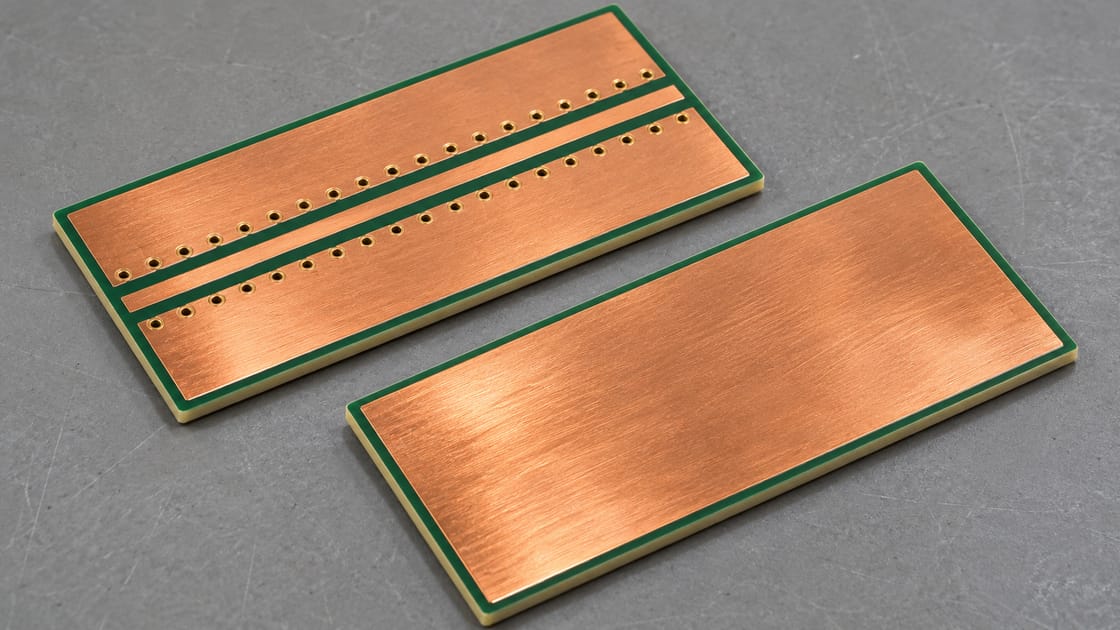
Real ground conductors have edges, and nearby metal can become part of the electromagnetic environment. An ideal model with infinitely wide grounds is not automatically representative of a narrow coupon inside an enclosure.
For the teaching feed, compare the side-ground width in the model with the actual copper remaining after component clearances and board cutouts. If the line is near a metal lid, include that boundary where it matters. A useful convergence check changes the modeled boundary distance or ground width and asks whether the answer has stabilized sufficiently for the design’s accuracy needs. Do not confuse solver precision with proof that omitted metal has no effect.
Use the Finished Etched Geometry, Not Only the Artwork
Etching can produce a conductor cross-section different from the ideal rectangle entered into a simple calculator. The gap that interacts with the fields is part of that finished geometry, not just an artwork dimension.
The Rogers–Sonnet comparison study discusses trapezoidal conductor shape and surface roughness in measured and modeled coplanar structures. Use that as evidence to request realistic geometry, not as a source of universal loss values. Ask which finished width and gap ranges the proposed process can support, then analyze those actual bounds rather than silently assuming the drawing’s nominal values are exact.
Keep Coatings and Finish Consistent With the Model
A model of bare copper and air does not fully describe a coated surface line. State whether mask covers the signal, the gaps and the nearby grounds, and what material model is being used.
Do not change a mask opening merely to make a calculator easier to use. Review electrical behavior, environmental protection and assembly needs together. The separate GCPW solder-mask guide focuses on that coating question. Here the first decision is still topology: a correct coating input does not rescue a calculation built on the wrong lower-plane assumption.
Verify the Straight Line and the Launch Separately
A uniform cross-section calculation does not verify a connector pad, bend, component discontinuity or the complete antenna match. Those features can require a different level of model and measurement.
Define the intended electrical acceptance before ordering: impedance, reflection, insertion loss and operating band are related but different requirements. If using a coupon, make its construction representative and state the measurement reference planes. When simulated and measured results differ, investigate the launch, fixture, material and finished geometry before assigning every discrepancy to trace width. The microstrip guide provides an adjacent reference for routes that do not intentionally use nearby side grounds.
Release a Cross-Section, Not Just a 50-Ohm Label
The release package must let the designer, fabricator and test team describe the same structure. A target number without topology and construction inputs leaves room for incompatible interpretations.
- Identify conventional CPW, connected GCPW or another explicit structure.
- Record the layer pair, lower-plane continuity and side-ground geometry.
- Confirm finished width, gap, copper and dielectric ranges.
- Keep mask, finish and material assumptions tied to the revision.
- Review vias, launch and discontinuities over the required band.
- Define coupon scope, measurement conditions and acceptance criteria.
For the teaching antenna feed, the correct next step is to rerun the appropriate model after adding bottom copper, not to preserve an old width because its original calculation said 50 ohms. Approve the resulting construction only after the required validation.
FAQ
Are CPWG, GCPW and CBCPW always different structures?
They are often used for the connected, conductor-backed coplanar arrangement, but naming conventions vary. Ask for a cross-section rather than resolving the design from an acronym alone. Verify the lower conductor, its connection to the side grounds and the model’s boundary assumptions before deciding that two calculators describe the same line.
Does copying a reference-board trace width guarantee 50 ohms?
No. The copied width must be considered with its original gap, dielectric separation, material, copper, coatings and ground geometry. A reference board may also use a different launch or stackup revision. Use its dimensions as design context, then validate the actual proposed construction instead of treating the width as a standalone component value.
Can a very short feed ignore the distinction?
Electrical length and the allowed error influence how much a discontinuity matters, but short physical length is not proof of equivalence. Review the operating band, surrounding structures and system requirements. A model mismatch should be understood and bounded even when the final engineering judgment accepts its effect as sufficiently small.
Does passing the CAD design-rule check verify the impedance?
Only the checks actually configured and implemented are verified. A clearance or connectivity rule can pass while the impedance model uses the wrong plane distance or topology. Inspect the rule’s purpose and the exported geometry. Treat electromagnetic validation and fabrication checks as complementary tasks, not interchangeable evidence for one another.
Is adding top ground beside microstrip always an improvement?
No automatic improvement follows from more copper. Nearby side conductors can change the line being built, especially when their gap is relevant to the fields. Review the revised structure and its connections. Keep a microstrip assumption only when the chosen analysis supports neglecting those conductors for the required accuracy and operating conditions.
Can a hatched lower plane be modeled as a solid plane?
Do not make that substitution without justification. The actual lower conductor pattern and its scale relative to the electrical behavior must be considered. A solver or calculation that assumes a continuous sheet may not represent the patterned structure. Use an appropriate model and validation plan rather than quietly changing the physical geometry in the analysis.
Why might two GCPW tools disagree with identical input numbers?
They may not use identical definitions or assumptions. Check whether gap and width refer to finished dimensions, how conductor thickness is represented, whether side grounds are finite, and which dielectric and coating models are used. Align those details before attributing the difference to numerical accuracy or selecting the more convenient answer.
Does good return loss prove low transmission loss?
No. A path can have limited reflection while still dissipating or radiating energy. Evaluate the separate performance requirements and use measurements appropriate to each. State the operating band, fixture and reference planes so a return-loss result is not presented as evidence that insertion loss or the complete antenna system also meets its target.
Discuss the RF Stackup
For a Best Technology manufacturing inquiry, send the proposed cross-section, layer stack, target impedance, operating band and coupon requirements to sales@bestpcbs.com. Confirm the construction and acceptance scope before treating nominal calculator dimensions as released production data.
You may also like


Tags: Coplanar Waveguide, GCPW, Impedance Modeling, RF PCB