





A higher thermal conductivity does not necessarily make an aluminum PCB dielectric a better heat path. For the same heat-flow area, a thicker layer can have more thermal resistance even if its material conducts heat better. Compare thickness divided by conductivity first, then verify isolation and the complete LED assembly.
Consider a hypothetical LED module mounted on an aluminum-backed board and a heatsink. Two proposed dielectrics differ in thickness and conductivity. The question is which option gives the lower ideal dielectric resistance without assuming either option meets the board’s electrical requirements.
Identify the Layer Between Copper and Aluminum
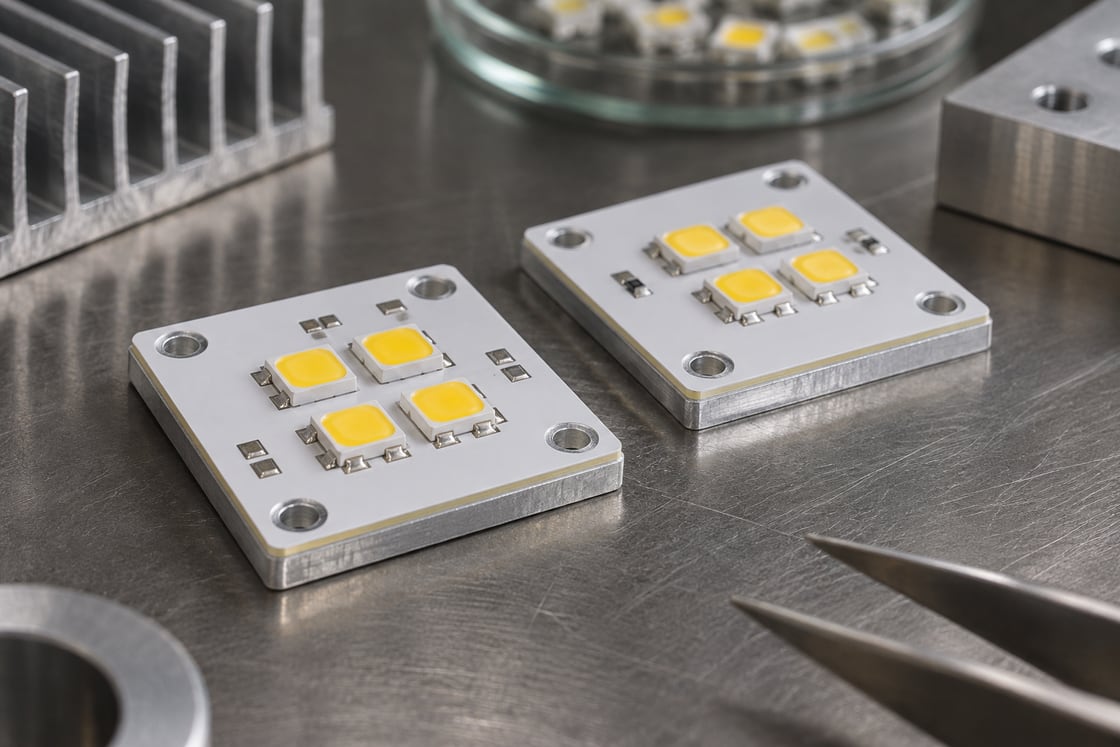
The dielectric separates the circuit copper from the metal base. It also lies in the heat path from the LED toward the heatsink. Do not use the thickness or conductivity of the aluminum base as a substitute for the dielectric’s properties.

Compare Material and Assembly Metrics
Use each metric for the object it describes. A material number, an ideal layer estimate and a complete module measurement answer different questions.
| Metric | Units | What it describes |
| Conductivity | W/(m·K) | Material heat conduction in the stated direction |
| Area-normalized layer resistance | m²·K/W | Ideal resistance multiplied by area |
| Thermal resistance | K/W | A specified path between two points |
Put Both Material Options on the Same Basis
Use actual thickness and through-plane conductivity for the construction. These numbers are hypothetical and do not describe commercial laminate grades.
| Parameter | Option A | Option B |
| Dielectric thickness | 75 µm | 150 µm |
| Through-plane conductivity | 1.5 W/(m·K) | 2.5 W/(m·K) |
| Ideal thickness divided by conductivity | 0.000050 m²·K/W | 0.000060 m²·K/W |
| Ideal resistance at 25 mm² | 2.0 K/W | 2.4 K/W |
Calculate Why Option B Loses in This Example
For one-dimensional conduction, divide thickness in meters by conductivity and area in square meters. Here 25 mm² is 0.000025 m². Option B conducts better as a material but is twice as thick; with equal area, its ideal layer resistance is 20% higher. The comparison ignores interfaces and spreading.
Confirm That the Published Values Use Compatible Methods
Check whether a supplier reports bulk conductivity, through-plane conductivity or the measured impedance of a constructed sample. A measured stack can include contributions absent from an ideal layer calculation. Use comparable test definitions and retain the source conditions.
Do Not Guess the Effective Heat-Flow Area
The LED thermal pad is a useful geometric reference, but heat can spread through copper and the metal base. The uniform area in the example isolates the effect of the dielectric. Use the real pad, copper layout and boundary conditions when the board decision needs more than a first estimate.
Check the Isolation Requirement Separately
A thinner dielectric does not automatically meet the application’s electrical requirements. Verify the construction-specific isolation requirements and the approved test method with the responsible team. Do not infer the finished board’s isolation from the material conductivity or from this thermal example.
Keep the Rest of the Heat Path in the Model
Include the LED package, solder interface, board, thermal interface to the sink and cooling conditions as appropriate. Cree LED’s thermal management note discusses the wider path from the LED into its surroundings. A small dielectric improvement may not dominate the complete assembly.
Compare the Board-to-Sink Joint Across Builds
Mount both options under comparable conditions. If a change in dielectric arrives with a change in mounting pressure, contact area or interface material, record those differences before attributing a measured change to the board. The result must identify what was actually tested.
Measure at Defined Reference Points
State the input power and operating conditions, then identify the temperature measurement points. A heatsink temperature alone does not establish junction temperature. Use the LED maker’s appropriate measurement or estimation method and verify whether the board and module limits are satisfied.
Treat a Supplier Substitution as a Construction Change
Request the new dielectric identity, thickness, conductivity basis and electrical data. Recalculate the comparison before accepting a replacement. If the construction differs materially, perform the agreed verification rather than substituting it because the advertised conductivity is higher.
Release Both Thermal and Electrical Evidence
Record the chosen build, thermal estimate assumptions, representative test and electrical acceptance. The Best Technology aluminum PCB thermal resistance guide covers the broader calculation; this comparison isolates the thickness-conductivity tradeoff.
FAQ
Is a thicker aluminum base the same as a thicker dielectric?
No. The base and the dielectric are distinct layers. Changing the aluminum may affect spreading and mechanics, while changing the dielectric directly alters a different portion of the path and can affect isolation. Check the stackup drawing before comparing a single thickness number.
Can I compare W per meter-kelvin with kelvins per watt?
Not directly. The first describes conductivity, while the second describes resistance for a specific path. Convert only when thickness and effective area are known under a suitable model. If a data sheet gives a measured resistance, check exactly what layers and interfaces it includes.
Does an area-normalized value include the heatsink interface?
It depends on what was measured or calculated. The example gives an ideal dielectric-only value and excludes the joint to the sink. A supplier’s measured result may use a different specimen and conditions. Compare the boundary and method before applying the number.
Can a higher-conductivity dielectric still reduce LED temperature?
Yes, if the actual construction lowers the relevant resistance and other conditions are comparable. Conductivity alone cannot tell you whether that happens because thickness, spreading and interfaces also matter. Test a representative board and mounting arrangement against the intended operating conditions.
Should I use the full board area in the formula?
Only if that area represents the heat flow in the assumed model. Heat from a small LED initially enters a local region and spreads through the construction. Using the full board area without justification may understate resistance. Document the area assumption and verify critical cases.
Does a lower calculated resistance prove better electrical isolation?
No. The thermal calculation does not measure electrical breakdown, leakage or compliance with the product’s requirements. Check the actual dielectric construction and qualification evidence. Keep the thermal and electrical pass decisions separate, even when the same material change affects both.
Why can two nominally identical modules run at different temperatures?
Assembly variables such as contact pressure, interface material coverage, solder condition and airflow can differ. Confirm the load and measurement locations first, then check the physical build. A difference in temperature is a reason to investigate, not proof of a dielectric problem.
What should I send for a material comparison?
Provide the stackup options, dielectric data and test conditions, LED footprint, heat input assumptions, and heatsink interface. Include electrical acceptance requirements and planned temperature observations. That package allows the reviewer to distinguish an ideal layer comparison from evidence about the finished module.
Prepare a Thermal Stackup Review
Send the dielectric options, LED footprint, mounting conditions and acceptance requirements to the Best Technology team.
You may also like



Tags: aluminum PCB dielectric, dielectric thickness, LED MCPCB, thermal resistance