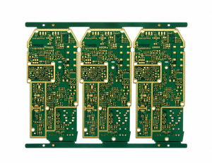
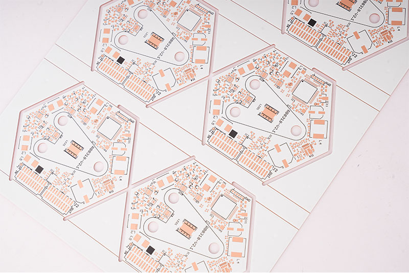
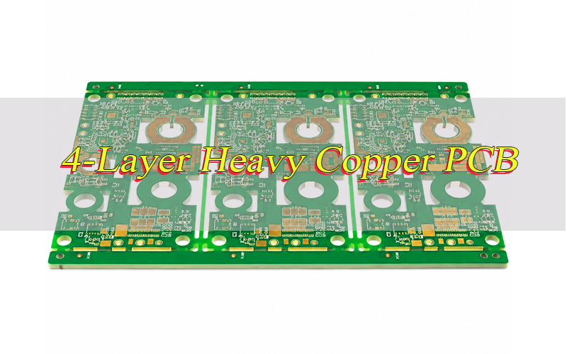
A 4-layer heavy copper PCB is built for circuits that handle high current, high heat and long operating time. It uses thicker copper than standard PCB structures, so the board can support stronger power paths, lower resistance and better heat spreading.
EBest provides custom 4-layer heavy copper PCB manufacturing, prototype and assembly support for power electronics, industrial control, medical devices, aerospace modules, EV systems, energy storage and high-power equipment.
Are you worried about these problems in 4-layer heavy copper PCB projects?
- Overheating risk: MOSFETs, terminals, relays, connectors and power ICs may generate local hot spots if the copper path is not designed correctly.
- Voltage drop risk: Narrow current paths, weak via design or poor copper distribution may reduce power efficiency.
- Manufacturing risk: Heavy copper increases etching difficulty, lamination stress, solder mask control and drilling requirements.
- Assembly risk: Thick copper absorbs more heat during soldering, which may affect solder wetting and joint quality.
With 20+ years of PCB manufacturing experience, EBest provides 4-layer heavy copper PCB manufacturing and assembly solutions for global power electronics, industrial equipment and engineering projects.
- Engineering review before production: Stackup, copper weight, current path, via structure and solder mask openings are checked before fabrication.
- Controlled heavy copper production: Etching, lamination, drilling, plating and electrical testing are controlled throughout production.
- Assembly process support: SMT process review, AOI inspection, functional testing and load-related inspection can be arranged based on project requirements.
If your project involves high current, tight reliability targets or strict production control, send your files to sales@bestpcbs.com for engineering review.
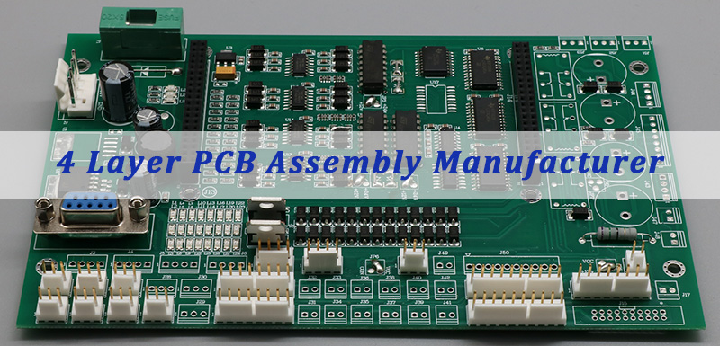
What Is a 4-Layer Heavy Copper PCB?
A 4-layer heavy copper PCB is a multilayer PCB with four conductive copper layers and thicker copper weight for high-current circuits. It is commonly used when standard 1 oz copper cannot safely carry the required current or manage heat.
In many projects, heavy copper starts from 2 oz to 3 oz, while higher-current boards may use 4 oz, 5 oz, 6 oz or more depending on the current path, board size and thermal target.
This structure allows engineers to separate power, ground, control and signal layers while keeping the board compact. For power electronics, this helps improve current flow, thermal stability and mechanical strength.
What Copper Thickness Is Common for a 4-Layer Heavy Copper PCB?
Copper thickness depends on current, temperature rise, trace width, board thickness and available routing space. For most 4-layer heavy copper PCB projects, copper weight usually ranges from 2 oz to 6 oz, while special power boards may require higher copper.
| Copper | Thickness | Common Use |
|---|---|---|
| 2 oz | 70 µm | Medium current power boards |
| 3 oz | 105 µm | Industrial control and power modules |
| 4 oz | 140 µm | High-current power distribution |
| 5 oz | 175 µm | Battery systems and motor drivers |
| 6 oz | 210 µm | High-load power electronics |
| 10 oz | 350 µm | Special high-current applications |
The best choice should be based on current load, allowed temperature rise, trace width and available PCB space, not only copper weight. Higher copper can carry more current, but it also increases spacing requirements, etching difficulty and production control requirements.
Why Choose a 4-Layer Heavy Copper PCB for High-Current Power Applications?
A 4-layer heavy copper PCB is chosen because it can carry higher current while keeping the layout more compact than a standard PCB. It also improves heat spreading and supports stronger power integrity.
Key advantages include:
- Higher current capacity: Thick copper reduces resistance in power paths.
- Better heat spreading: Larger copper mass helps move heat away from power components.
- Compact power layout: Four layers allow better routing than single-sided or double-sided boards.
- Improved reliability: Stronger copper paths reduce overheating and voltage drop.
- Better mechanical strength: Heavy copper improves board durability in demanding equipment.
This PCB type is suitable when the product must operate safely under high load, vibration, heat or continuous power cycling.
Where Are 4 Layers Heavy Copper PCBs Commonly Used?
4-layer heavy copper PCBs are used in products that require stable current delivery, strong thermal performance and long-term reliability. They are common in power electronics and industrial equipment.
Common applications include:
- Industrial control: Motor drives, power controllers, automation equipment and welding systems.
- EV and energy systems: Battery management systems, charging modules and power distribution boards.
- Medical equipment: Imaging power modules, surgical devices and diagnostic control boards.
- Aerospace electronics: Power regulation modules, control units and high-reliability power boards.
- Telecom power systems: Base station power modules and high-current conversion boards.
- LED and lighting systems: High-power lighting drivers and thermal control boards.
For these industries, the board must support current, heat, insulation and reliability at the same time.
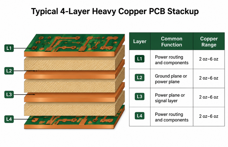
What Is the Typical 4-Layer Heavy Copper PCB Stackup?
A typical 4-layer heavy copper PCB stackup uses two outer copper layers and two inner copper layers. The stackup is usually designed to separate power, ground and signal functions while controlling heat and current flow.
| Layer | Common Function | Copper Range |
|---|---|---|
| L1 | Power routing and components | 2 oz–6 oz |
| L2 | Ground plane or power plane | 2 oz–6 oz |
| L3 | Power plane or signal layer | 2 oz–6 oz |
| L4 | Power routing and components | 2 oz–6 oz |
A practical stackup may use outer layers for power components, inner layers for ground or current return, and thick copper planes for heat spreading. The final structure should match component placement, current direction and assembly requirements.
What Materials and Surface Finishes Are Used for 4-Layer Heavy Copper PCBs?
A 4-layer heavy copper PCB usually uses high-Tg FR4, heavy copper foil, reliable prepreg and a surface finish suitable for soldering. Material selection affects heat resistance, lamination quality and long-term stability.
| Item | Common Option | Typical Selection |
|---|---|---|
| Base material | High-Tg FR4 | Tg 150°C–180°C |
| Copper weight | 2 oz–6 oz | Higher for power paths |
| Board thickness | 1.6 mm–3.2 mm | Based on current and structure |
| Surface finish | ENIG, HASL, OSP | Based on assembly needs |
| Solder mask | High-temperature mask | Better insulation and protection |
| Finished copper | IPC controlled | Based on final performance target |
ENIG is often selected for fine-pitch assembly and stable solderability. HASL can be used for less complex power boards, while OSP may suit selected SMT projects.
How to Design a 4-Layer Heavy Copper PCB for High Current?
Designing a 4-layer heavy copper PCB for high current starts with current flow, heat control and manufacturability. The layout should begin from the power path, return path, copper thickness and expected temperature rise.
Step 1: Confirm the current, voltage and temperature rise target.
Before layout, confirm the maximum current, continuous current, peak current, working voltage and allowed temperature rise. A board carrying 10A, 30A or 80A cannot use the same copper width, via quantity or connector design. If the current is continuous, the copper path must be more conservative than a short-pulse circuit.
Step 2: Choose the correct copper thickness for each layer.
For a custom 4-layer heavy copper PCB, common copper thickness includes 2 oz, 3 oz, 4 oz, 5 oz and 6 oz. Higher copper supports stronger current flow, but it also increases etching difficulty, spacing requirements and solder mask control. In many projects, outer layers carry high-current components, while inner layers work as power planes or ground return layers.
Step 3: Plan the stackup early.
A practical stackup should separate power, ground, control and signal functions. For example, L1 can carry power components and short high-current traces, L2 can work as a ground plane, L3 can work as a power plane, and L4 can support additional power routing or control circuits. The final stackup should match the real current direction, not only layer symmetry.
Step 4: Keep the high-current path short and wide.
High-current traces should be short, direct and wide. Avoid narrow neck-down areas near connectors, fuses, MOSFETs, relays, shunts and terminal blocks. A small bottleneck in one area can create local heating even when the rest of the copper path is wide enough.
Step 5: Use copper planes instead of only traces.
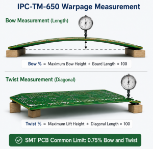
For high-current power applications, copper planes are usually better than long narrow traces. A large copper plane reduces resistance, spreads heat and lowers voltage drop. However, copper distribution should remain balanced across layers to reduce warpage during lamination and reflow.
Step 6: Design enough vias for layer-to-layer current sharing.
When current moves between layers, one via is not enough for high-current paths. Use multiple vias in parallel near connectors, MOSFET drains, power terminals and current return areas. The via diameter, finished hole size, copper plating thickness and via quantity should be reviewed together.
Step 7: Place heat-generating components with thermal flow in mind.
MOSFETs, rectifiers, regulators, relays, shunts and high-current connectors should not be crowded in one small area. Leave enough copper around them for heat spreading. If the product uses a housing, heatsink or chassis, place thermal areas where heat can transfer to the mechanical structure.
Step 8: Control return current paths.
The return path is as important as the positive power path. A poor return path can increase loop area, voltage drop, EMI risk and local heating. Place power and return paths close where possible, and use solid ground or return planes for stable current flow.
Step 9: Check creepage and clearance for high voltage.
High current and high voltage often appear together in power electronics. Increase spacing between power nets, exposed copper, board edges, mounting holes and metal hardware. Do not apply standard low-voltage PCB spacing to industrial, EV, medical or aerospace power boards.
Step 10: Review assembly before finalizing the layout.
Heavy copper absorbs more heat during soldering. Large pads, power terminals and thermal areas may need adjusted stencil openings, solder paste volume and reflow profiles. Pad design should support stable soldering, not only electrical performance.
Step 11: Run DFM review before prototype production.
Before making a 4-layer thick copper PCB prototype, check trace width, spacing, copper balance, via design, solder mask bridge, annular ring, board thickness, surface finish and assembly risk. This step helps avoid repeated prototype changes and improves first-pass success.
A strong high-current design is not only about using thicker copper. It depends on current path planning, copper balance, thermal spreading, via strategy, insulation safety and assembly process control working together.
What Design Rules Should Be Followed for a 4-Layer Heavy Copper PCB?
A 4-layer heavy copper PCB should follow stricter design rules than a standard FR4 PCB because thick copper affects etching, lamination, drilling, solder mask coverage and soldering stability. The design should be reviewed before production, especially for high-current power applications.
- Use wider trace spacing for heavy copper.
Thick copper is harder to etch than standard 1 oz copper. If spacing is too tight, the risk of copper residue, short circuits and line width deviation increases. Higher copper weight usually requires larger spacing. - Avoid narrow current bottlenecks.
A wide copper plane can still overheat if the current passes through one narrow trace, small pad neck or limited connector area. Check every transition point in the current path. - Use multiple vias for high-current transfer.
Current should not depend on one or two vias when moving between layers. Use via arrays for current sharing, and place them close to the power pad or copper plane transition. - Increase annular ring and pad size where possible.
Heavy copper PCB drilling and plating require stronger tolerance control. Larger annular rings help improve hole reliability, especially around terminals, connectors and high-current plated holes. - Keep copper balanced across layers.
Uneven copper distribution may cause board warpage, lamination stress and assembly issues. Try to balance large copper areas between layers and avoid one-sided copper concentration. - Review solder mask bridge width.
Heavy copper creates a higher copper step. If the solder mask bridge is too narrow, mask alignment and coverage may become unstable. Larger spacing improves solder mask reliability. - Control creepage and clearance.
For high-voltage power circuits, spacing must consider voltage, contamination level, coating, operating environment and safety requirements. Board edge clearance and mounting hole clearance should also be checked. - Use thermal relief carefully.
Standard thermal relief may reduce soldering stress, but it can also restrict current and heat flow. For power pads, choose direct connection or adjusted thermal relief based on soldering and electrical needs. - Avoid sharp copper corners in power areas.
Rounded or softened copper corners help reduce current crowding and manufacturing stress. This is useful around heavy copper planes, large pads and high-current terminals. - Confirm connector pad and terminal design.
High-current connectors need enough copper area, mechanical support and soldering strength. Pad size, hole diameter and copper plating should match the real connector specification. - Separate power and sensitive signal routing.
High-current switching areas can create noise. Keep sensing lines, feedback traces and low-level signals away from switching nodes, relays, MOSFET drains and high-current loops. - Check finished copper, not only starting copper.
PCB fabrication changes copper thickness through plating and processing. The design should confirm finished copper thickness, especially for high-current paths and plated holes. - Confirm manufacturability before releasing Gerber files.
Design rules vary by copper thickness, board thickness, layer structure and surface finish. EBest reviews these details before production to reduce etching risk, lamination defects and soldering problems.
These rules help improve current capacity, heat control, insulation safety, soldering quality and production yield.
How Does Thermal Management Affect 4-Layer Heavy Copper PCB Performance?
Thermal management directly affects current capacity, component life and field reliability. A 4-layer heavy copper PCB can spread heat better than a standard PCB, but poor layout can still create hot spots.
Effective thermal control includes:
- Large copper areas around MOSFETs, rectifiers, relays and connectors.
- Thermal vias between power layers and heat-spreading layers.
- Balanced copper distribution to reduce warpage during production.
- Proper component spacing to prevent heat concentration.
- Controlled solder mask openings for power pads and exposed copper.
- Mechanical heat transfer through screws, chassis contact or heat sinks when required.
The design should be reviewed under real operating current, not only room-temperature electrical conditions.
What Should Be Confirmed Before 4-Layer Heavy Copper PCB Production?
Before production, the engineering team should confirm copper thickness, stackup, board thickness, current path, spacing, via structure and assembly requirements. This avoids production delays and performance risks.
Confirm these items before release:
- Gerber and drill files
- Copper weight for each layer
- Finished board thickness
- Minimum trace width and spacing
- Current and voltage requirements
- Surface finish
- Solder mask opening
- Via type and via quantity
- Controlled impedance if required
- Assembly drawing and BOM
- Testing requirements
For high-current applications, EBest reviews manufacturability before fabrication to reduce etching issues, soldering defects and batch variation.
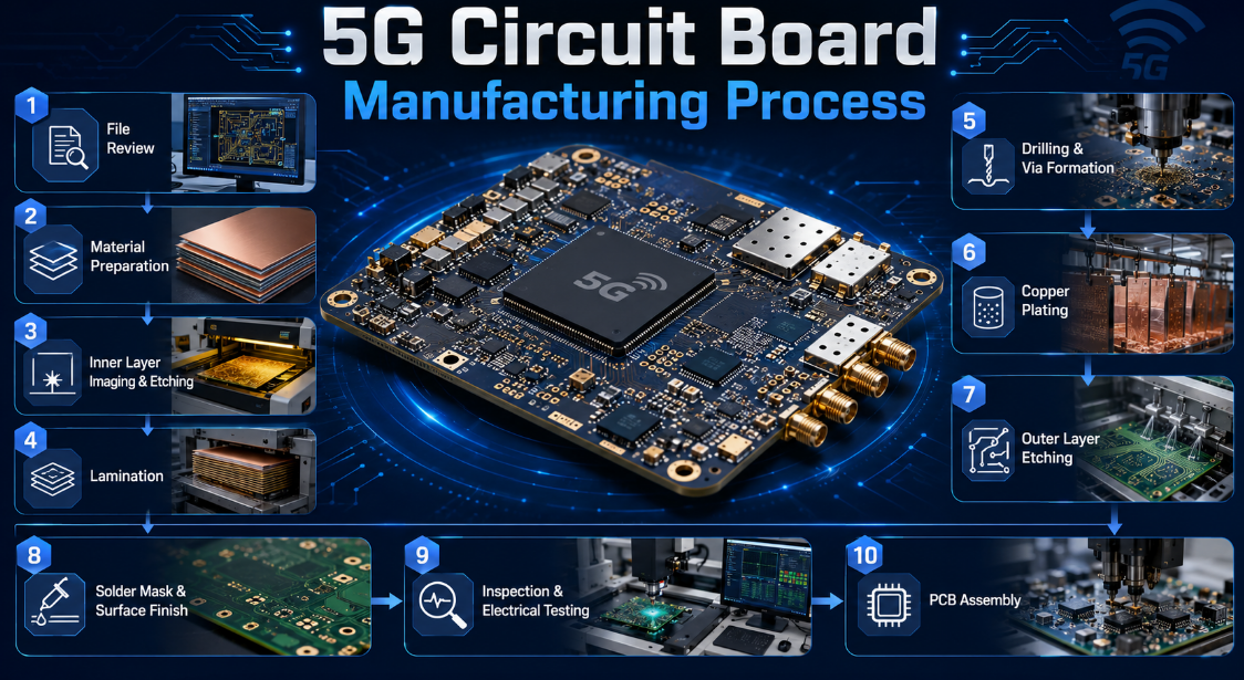
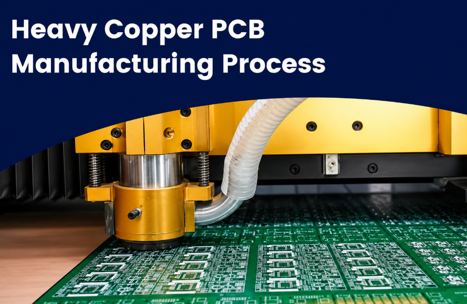
How Does the 4-Layer Heavy Copper PCB Manufacturing Process Work?
The 4-layer heavy copper PCB manufacturing process is more demanding than standard multilayer PCB production. Thick copper requires stronger control in etching, lamination, drilling, plating, solder mask and final inspection.
Step 1: Engineering review and DFM checking.
The process starts with Gerber review, drill file review, stackup confirmation and copper thickness checking. Engineers check whether the trace width, spacing, hole size, annular ring, copper balance and solder mask design match heavy copper production capability.
Step 2: Material preparation.
The factory prepares high-Tg laminate, copper foil, prepreg and process materials according to the approved stackup. For high-current applications, material selection must support heat resistance, insulation strength and mechanical stability.
Step 3: Inner layer imaging.
The inner copper layers are cleaned, coated with photoresist and exposed according to the circuit pattern. These layers often include power planes, ground planes or high-current distribution areas.
Step 4: Inner layer etching.
The unwanted copper is removed to form the inner layer circuit. Heavy copper etching must control line width and spacing carefully because thicker copper takes longer to etch and may create side etching.
Step 5: Inner layer inspection.
After etching, AOI inspection checks opens, shorts, copper residue and pattern accuracy. This step is important because inner layer defects cannot be repaired easily after lamination.
Step 6: Oxide treatment and lamination preparation.
The inner layers are treated to improve bonding strength. Then copper layers, prepreg and core materials are stacked according to the approved stackup.
Step 7: Lamination.
Heat and pressure bond the four-layer structure together. Heavy copper areas create deeper copper gaps, so resin flow and filling must be controlled. Poor resin filling can cause voids, delamination or insulation weakness.
Step 8: Drilling.
After lamination, CNC drilling creates plated through holes, vias and mounting holes. Heavy copper and thicker boards increase drilling stress, so drill parameters must be controlled to protect hole wall quality.
Step 9: Desmear and hole metallization.
The drilled holes are cleaned, and the hole walls are prepared for copper deposition. This step supports reliable electrical connection between layers.
Step 10: Copper plating.
Copper is plated inside the holes and on outer layers. Plating thickness must be stable because vias and plated holes may carry current between layers. Poor plating can increase resistance or cause field failure.
Step 11: Outer layer imaging and etching.
The outer circuit is transferred and etched. Heavy copper outer layers need accurate process control to prevent under-etching, over-etching, copper residue and uneven line width.
Step 12: Solder mask application.
Solder mask protects copper and prevents solder bridging. Heavy copper has a higher surface step, so solder mask thickness, coverage and alignment must be inspected carefully.
Step 13: Surface finish.
The board receives ENIG, HASL, OSP or another approved finish. The surface finish should match component type, soldering method, shelf-life requirement and assembly process.
Step 14: Routing and profiling.
The board outline, slots and mechanical features are routed. For heavy copper boards, edge quality and copper exposure should be checked to avoid insulation and handling issues.
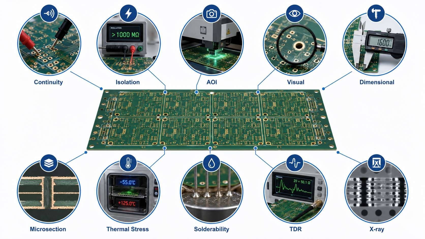
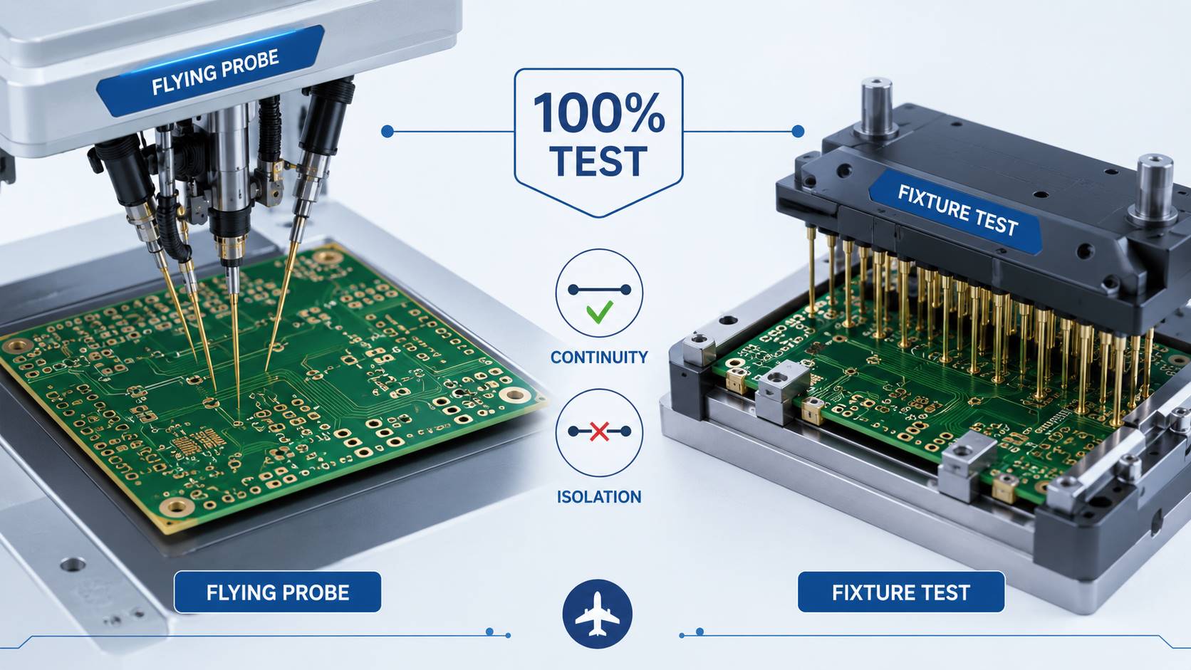
Step 15: Electrical testing.
Each board is tested for open circuits, short circuits and netlist accuracy. For high-current designs, additional customer-specified tests may be added.
Step 16: Final inspection and packaging.
The final boards are inspected for appearance, thickness, solder mask, surface finish, hole quality, routing accuracy and cleanliness. Boards are packed to protect copper surface, solderability and mechanical condition.
This process helps ensure that the board can support high current, stable soldering and reliable long-term operation.
What Manufacturing Challenges Affect 4-Layers Heavy Copper PCB Quality?
The main manufacturing challenges are etching control, lamination filling, copper balance, drilling quality and solder mask coverage. Heavy copper is thicker, so normal PCB process windows may not be enough.
Common challenges include:
- Etching deviation: Thick copper can cause wider line variation.
- Insufficient resin filling: Heavy copper gaps need proper lamination control.
- Copper imbalance: Uneven copper may cause warpage.
- Drilling stress: Thick copper and multilayer structure increase drilling difficulty.
- Solder mask edge coverage: High copper steps can affect mask thickness.
- Plating uniformity: Vias must support stable layer connection.
- Assembly heat absorption: Heavy copper may require adjusted soldering profiles.
These risks can be reduced through DFM review, controlled stackup and process inspection.
How Do We Control Quality for 4-Layers Heavy Copper PCB Manufacturing?
EBest controls heavy copper PCB quality from engineering review to final shipment. The goal is to prevent high-current failure, overheating, poor soldering, insulation weakness and batch instability before the board reaches the customer.
Engineering quality control starts before production.
We review Gerber files, drill files, stackup, copper thickness, board thickness, trace width, spacing, via structure, annular ring, solder mask openings and surface finish. If the design has high-current bottlenecks, risky spacing or difficult heavy copper features, our engineering team gives feedback before fabrication.
Material control protects long-term reliability.
Heavy copper boards require stable laminate, copper foil and prepreg. We check material type, copper weight, board thickness and production compatibility before processing. For high-power applications, material selection affects thermal performance, insulation strength and lamination stability.
Inner layer inspection reduces hidden defects.
Inner layers are inspected before lamination. AOI checks circuit pattern, shorts, opens, copper residue and line accuracy. This step is critical because inner layer defects become difficult to identify after multilayer bonding.
Lamination control prevents resin voids and delamination.
Heavy copper creates larger copper height differences than standard PCB. We control lamination pressure, temperature, resin flow and copper balance to reduce voids, weak bonding and thickness instability.
Drilling and plating inspection protects layer connection.
Vias and plated holes are important for current sharing between layers. We inspect drilling quality, hole wall condition and copper plating quality to reduce resistance, cracking and intermittent connection risks.
Solder mask inspection improves assembly stability.
Heavy copper steps can affect solder mask coverage. We check mask alignment, bridge width, edge coverage and exposed copper risk. This improves insulation and reduces solder bridging during assembly.
Electrical testing confirms circuit accuracy.
Finished boards are tested for continuity, open circuits and short circuits. For critical high-current projects, customer-specified current load testing, insulation testing or functional testing can be arranged.
Assembly quality control supports turnkey projects.
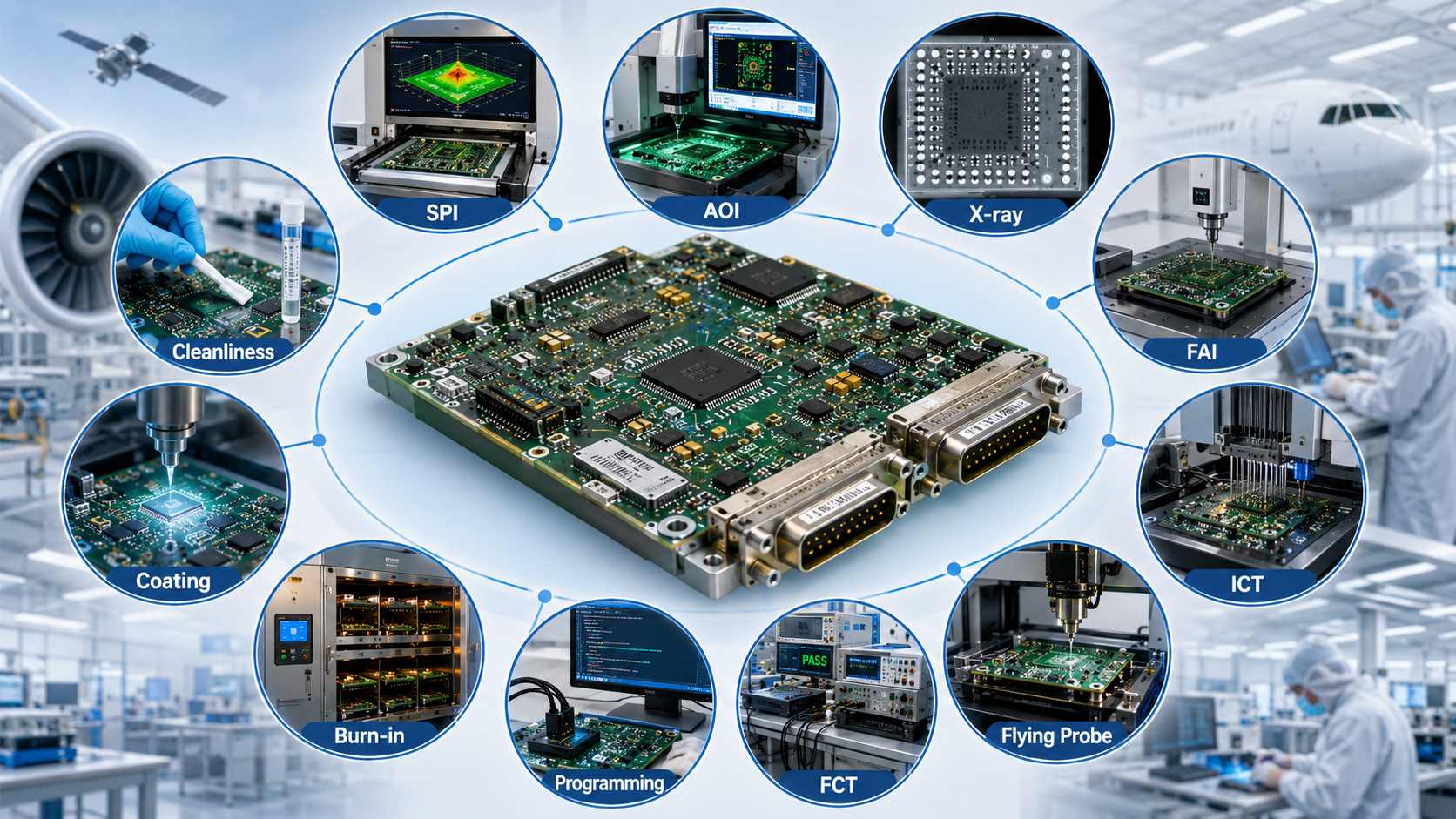
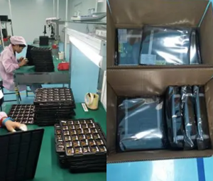
For assembled heavy copper PCBs, EBest can support SPI, AOI, X-ray inspection when required, polarity checks, solder joint inspection, functional testing and final visual inspection. Reflow profiles are reviewed because heavy copper absorbs more heat than standard PCB copper.
Final inspection protects shipment quality.
Before delivery, we check board appearance, dimensions, thickness, surface finish, solder mask, marking, cleanliness, quantity and packaging. The final goal is stable delivery and consistent batch quality.
Through engineering review, material inspection, process control and final testing, EBest helps customers improve reliability in industrial control, medical electronics, aerospace power modules, EV systems and high-current power equipment.
Case Study: 4-Layer Heavy Copper PCB for High-Current Power Applications
This project was a custom 4-layer heavy copper PCB for an industrial high-current power control module. The customer needed stable current flow, lower heat concentration and reliable prototype validation before batch production.
Project Background
The PCB was used in industrial power equipment with MOSFETs, high-current terminals, protection circuits and control components. The board size was limited, but the current load was high.
The customer was concerned about voltage drop, overheating around power components and soldering stability during assembly. They wanted to build a 4-layer thick copper PCB prototype first to confirm the design before mass production.
Project Requirements
The project required:
- Stable high-current carrying capacity
- Lower voltage drop on the main power path
- Better heat spreading around MOSFETs and terminals
- Reliable via design for layer-to-layer current sharing
- Balanced copper distribution to reduce warpage risk
- Stable SMT assembly quality
- Prototype validation before batch production
Our Solution
EBest reviewed the Gerber files, drill files, stackup, copper thickness and assembly requirements before production. Our engineering team checked the high-current paths, via quantity, copper balance, solder mask openings and thermal layout.
We found that some power paths were too narrow, and the via quantity was not enough for stable current sharing. The copper distribution also needed improvement to reduce production and assembly risk.
EBest optimized the design by:
- Widening the main power copper paths
- Adding more vias near high-current transitions
- Increasing copper area around MOSFETs and terminals
- Improving copper balance across four layers
- Reviewing solder mask openings for power pads
- Controlling heavy copper etching, lamination, drilling and plating
- Checking SMT assembly conditions for heavy copper heat absorption
After confirmation, EBest produced the prototype and completed electrical testing, visual inspection and assembly inspection.
Output Results
The prototype passed PCB inspection, electrical testing and assembly inspection. Customer-side validation showed better current stability and reduced heating risk near the connector and MOSFET area.
The final results included:
- More stable current flow
- Lower local heating risk
- Better layer-to-layer current sharing
- Improved production stability
- Reliable SMT assembly quality
- Prototype approval before batch production
This case shows that a reliable result depends on copper thickness, stackup review, current path planning, via design, thermal layout and manufacturing control.
Why Choose EBest as Your 4-Layer Heavy Copper PCB Manufacturer?
Choose EBest for projects that require design review, prototype testing, mass production and assembly support. Here are reasons why choose us as your 4-layer heavy copper PCB manufacturer:
- 20+ years of PCB experience
EBest was founded in 2006. Our team supports custom PCB projects from early file review to final delivery. - One-stop PCB service
EBest provides PCB Design, PCB Prototype, Mass Production, Component Sourcing and PCB Assembly. This helps customers manage fabrication, prototype validation, sourcing, assembly and testing through one supplier. - Heavy copper production capability
EBest manufactures heavy copper boards for power control boards, motor drives, EV modules, industrial equipment, medical electronics and aerospace control systems. - Engineering review before production
We check Gerber files, drill files, stackup, copper weight, trace width, spacing, annular ring, via structure, solder mask openings and surface finish before fabrication. - Prototype and production support
EBest can produce prototypes for current testing, solderability checking, thermal validation and assembly review before mass production. - Monthly production capacity
EBest has a monthly production capability of about 260,000 square feet, equal to around 28,900 square meters. - Expedited service for urgent projects
Urgent orders can be supported when files, materials and process conditions are confirmed. - Certified quality system
EBest holds ISO 9001:2015, IATF 16949, ISO 13485:2016, AS9100D, UL, RoHS and REACH certifications. - Fabrication and assembly control
Heavy copper absorbs more heat during soldering. EBest reviews pad design, stencil openings, soldering conditions, AOI inspection and functional testing to improve assembly quality.
What Files Are Needed for a Custom 4-Layer Heavy Copper PCB Quote?
For a custom quote, provide complete fabrication and assembly data. Clear files help engineers review stackup, copper thickness, design rules and production risk quickly.
Required files include:
- Gerber files
- Drill files
- PCB stackup
- Copper thickness for each layer
- Board thickness
- Material requirement
- Surface finish
- Solder mask color
- Silkscreen color
- Current and voltage data
- Assembly drawing
- BOM
- Pick-and-place file
- Testing requirement
- Quantity requirement
For high-current power applications, also provide expected current, working temperature, connector type, thermal requirement and any reliability standard required by the final product.
FAQs About 4 Layer Heavy Copper PCB
Q1: What is a 4-layer heavy copper PCB used for?
A1: It is used for high-current and high-heat circuits, such as motor drives, power supplies, EV charging modules, battery systems, industrial controllers, medical power modules and aerospace control boards.
Q2: What copper thickness is common for a 4-layer heavy copper PCB?
A2: Common copper thickness is 2 oz to 6 oz. Special high-current boards may use 10 oz or higher, depending on current, trace width, temperature rise and board size.
Q3: Is 4 oz copper enough for high-current applications?
A3: It depends on current, trace width, via design and working temperature. 4 oz copper is about 140 µm thick, but poor layout can still cause overheating.
Q4: Why is stackup important in a 4-layer heavy copper PCB?
A4:. Stackup affects current flow, heat spreading, return path and production stability. A proper stackup helps separate power, ground and control layers.
Q5: What design mistake often causes overheating?
A5: A narrow current bottleneck is the most common issue. Small trace necks, weak connector pads or too few vias can increase resistance and create local hot spots.
Q6: Can EBest make a 4-layer thick copper PCB prototype?
A6: Yes. EBest supports prototype production for current testing, thermal checking, solderability review and assembly validation.
Q7: Does heavy copper PCB need special assembly control?
A7: Yes. Heavy copper absorbs more heat than standard PCB copper. Reflow profile, solder paste volume, stencil design and solder joint inspection should be reviewed before assembly.
Q8: Can this type of PCB be used in medical or aerospace products?
A8: Yes. It can be used in medical power modules, imaging equipment, aerospace control systems and high-reliability power boards.
Q9: Is a 4-layer heavy copper PCB the same as a copper base PCB?
A9: No. A 4-layer heavy copper PCB uses thick copper layers for current carrying. A copper base PCB uses a copper metal base or copper core mainly for heat dissipation.
EBest Circuit provides custom multi-layer heavy copper PCB manufacturing, PCB prototype support, stackup review, design rule checking and assembly service for high-current power applications. If you need a reliable multi-layer heavy copper PCB manufacturer for industrial equipment, medical electronics, aerospace modules, EV systems, power control boards or energy products, send your project files to sales@bestpcbs.com.