

What exactly is stitch bond in chip packaging, and why is it a foundational process in modern semiconductor assembly? For engineers navigating packaging design, understanding this interconnect method is critical for optimizing yield, reliability, and cost. This article breaks down stitch bond fundamentals, compares it to ball bond, and addresses core challenges to help you make informed decisions for your projects.
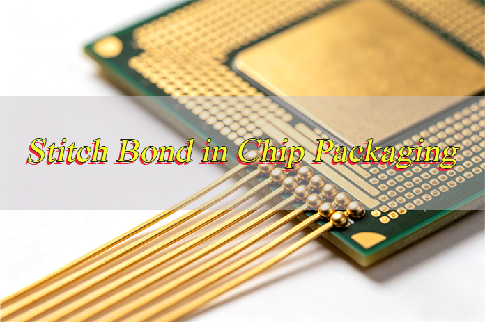
What is Stitch Bond in Chip Packaging?
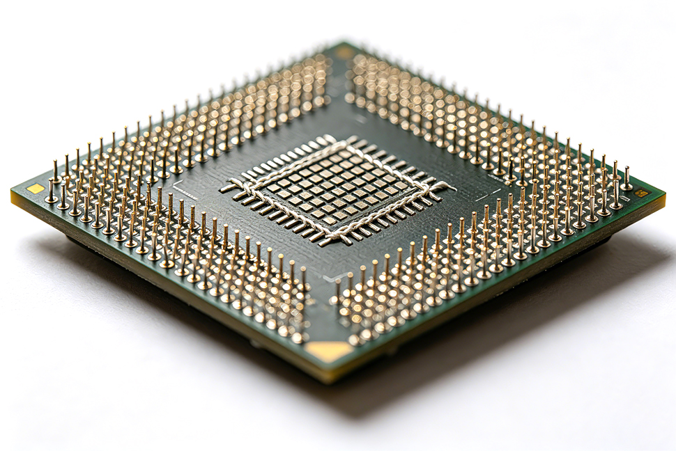
Stitch bond in chip packaging is a wire bonding technique that forms the second connection (second bond) between a metal wire and a substrate or lead frame, following the first bond on the chip pad. Also called a wedge bond or tail bond, it creates a flat, stitch-like joint by compressing the wire with a capillary tool, often with heat and ultrasonic energy.
As a key part of thermosonic wire bonding, it works alongside ball bond to establish electrical pathways between the chip and external circuits. Stitch bond in chip packaging is distinct from ball bond in its joint shape, formation process, and mechanical properties.
It is the most common second bond method in high-volume packaging, used in over 80% of traditional wire-bonded ICs.
How Does Stitch Bond in Chip Packaging Work in Semiconductor Assembly?
Stitch bond in chip packaging operates as the final step in the wire bonding cycle, following ball bond formation on the chip. The process starts with an electronic flame-off (EFO) that melts the wire tip into a free-air ball (FAB). The capillary tool presses the ball onto the chip pad to form the first bond (ball bond).
The capillary then rises, forms a precise wire loop, and moves to the target substrate pad. At the second bond site, the capillary compresses the wire withheat (150–250°C), ultrasonic vibration (60–120 kHz), and pressure (50–200 gf).
This crushes the wire into a flat, stitch-shaped joint, shears the wire, and leaves a small tail for the next cycle. The result is a robust mechanical and electrical connection. Key steps include:
1. EFO ball formation at the wire tip.
2. First bond (ball bond) on the chip pad.
3. Wire loop formation and capillary movement to the substrate.
4. Stitch bond formation via compression, heat, and ultrasound.
5. Wire shearing and tail retention for the next bond.
What Materials Are Used for Stitch Bond in Chip Packaging?
Stitch bond in chip packaging relies on high-conductivity, ductile metals that form reliable bonds under thermosonic conditions. The most common materials are:
- Gold (Au) Wire: The traditional standard. Excellent ductility, oxidation resistance, and bondability. Ideal for fine-pitch applications (25–50 μm diameter).
- Copper (Cu) Wire: The dominant modern choice. Lower cost than gold, higher tensile strength, and better electrical conductivity. Requires a nitrogen-hydrogen atmosphere to prevent oxidation.
- Palladium-Coated Copper (Pd-Cu) Wire: Combines copper’s cost benefits with palladium’s oxidation resistance. Reduces corrosion risks in harsh environments.
- Aluminum (Al) Wire: Used for ultrasonic wedge bonding at room temperature. Common in power devices and automotive applications.
Substrates and lead frames also matter. Stitch bond in chip packaging typically bonds to copper lead frames, ceramic substrates, or organic PCBs with gold or palladium plating.
What Equipment is Needed for Stitch Bond in Chip Packaging?
Stitch bond in chip packaging requires precision wire bonding machines and specialized tools. Core equipment includes:
- Thermosonic Wire Bonder: The primary machine. Integrates EFO, capillary movement, heat control, and ultrasonic generators. Achieves accuracies of ±1 μm.
- Capillary Tool: A tiny ceramic or tungsten needle with a central hole for the wire. Its tip geometry (angle, diameter) directly impacts stitch bond quality.
- Heated Workholder: Maintains substrate temperature at 150–250°C to enhance bond formation.
- Ultrasonic Generator: Delivers high-frequency vibration to the capillary, breaking surface oxides and promoting metal diffusion.
- Wire Feeder & Spool: Holds the metal wire and feeds it through the capillary at controlled tension.
- Inspection System: Uses optical or SEM imaging to verify stitch bond integrity, loop height, and wire alignment.
Advanced systems add automated wire changing, real-time process monitoring, and AI-driven defect detection for high-volume production.
What Are the Applications of Stitch Bond in Chip Packaging?
Stitch bond in chip packaging is ubiquitous across semiconductor packaging, serving diverse industries and device types. Key applications include:
- Consumer Electronics: Smartphones, wearables, and memory chips (DRAM, Flash) use fine-pitch stitch bonds for compact, high-density interconnects.
- Automotive Semiconductors: ECUs, sensors, and power modules rely on stitch bond’s mechanical stability and resistance to temperature cycling.
- Industrial & Power Devices: MOSFETs, IGBTs, and rectifiers use heavy-gauge copper wire stitch bonds for high-current, high-temperature operation.
- Medical Devices: Implantable sensors and diagnostic ICs use gold wire stitch bonds for biocompatibility and reliability.
- Aerospace & Defense: High-reliability ICs for avionics and satellites use stitch bonds to withstand extreme vibration and thermal stress.
It is used in all traditional wire-bonded packages: DIP, SOP, QFP, SOIC, and BGA (for wire-bonded BGAs).
What Are the Advantages of Stitch Bond in Chip Packaging?
Stitch bond in chip packaging offers unique benefits that make it indispensable in modern assembly. Key advantages include:
- High Mechanical Strength: The flat, compressed joint provides a large bonding area, delivering pull strengths of 5–15 gf (gold wire) and 10–25 gf (copper wire).
- Cost Efficiency: Copper wire stitch bonds reduce material costs by 30–50% compared to gold ball bonds.
- Fine Pitch Capability: Supports pad pitches as small as 40 μm, critical for miniaturized devices.
- Process Flexibility: Compatible with gold, copper, and aluminum wires; works on diverse substrates (copper, ceramic, PCB).
- High Throughput: Modern bonders achieve 8–12 bonds per second, ideal for mass production.
- Loop Height Control: Enables precise, low-profile wire loops (50–200 μm) to avoid mold flash and improve package density.
What Are the Common Challenges of Stitch Bond in Chip Packaging?
Despite its benefits, stitch bond in chip packaging faces persistent challenges that impact yield and reliability. Key issues include:
- Bond Lifting: Insufficient heat, ultrasound, or surface contamination causes the stitch bond to peel from the substrate.
- Wire Breakage: Excessive tension, improper loop formation, or capillary damage leads to wire fracture at the stitch site.
- Substrate Damage: High pressure or ultrasonic energy can crack brittle ceramic substrates or damage thin copper plating.
- Oxidation: Copper wires oxidize rapidly without inert gas protection, weakening bonds and increasing resistance.
- Pitch Limitations: Below 40 μm pitch, capillary interference and wire bridging become critical issues.
- Thermal Stress: Mismatched coefficients of thermal expansion (CTE) between wire and substrate cause bond fatigue in temperature cycling.
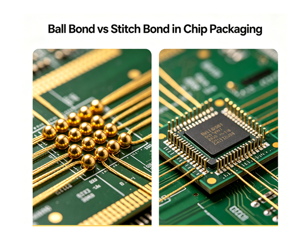
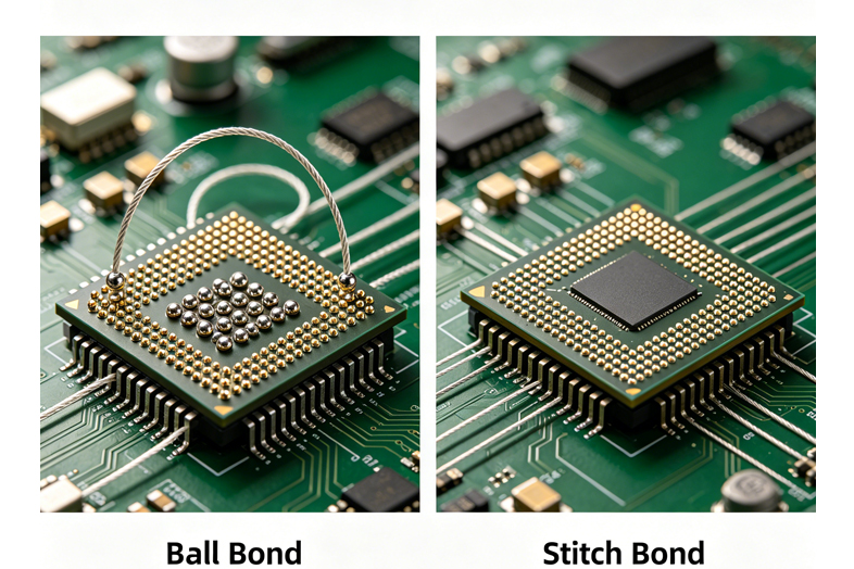
What is the Difference Between a Ball Bond and a Stitch Bond?
Ball bond and stitch bond in chip packaging are the two core wire bonding steps, differing in formation, shape, and function. The table below summarizes key differences:
| Feature | Ball Bond | Stitch Bond |
| Bond Position | First bond (chip pad) | Second bond (substrate/lead frame) |
| Formation Method | EFO melts wire tip into a ball; pressed onto pad | Capillary compresses wire into a flat stitch; shears wire |
| Shape | Spherical or hemispherical | Flat, wedge-shaped, stitch-like |
| Key Energy | Heat + ultrasound + pressure | Heat + ultrasound + pressure (higher compression) |
| Wire Type | Gold, copper, Pd-Cu | Gold, copper, Pd-Cu, aluminum |
| Primary Function | Secure chip-side connection; enable loop formation | Secure substrate-side connection; complete electrical path |
| Typical Strength | 10–20 gf (gold) | 5–15 gf (gold) |
In short, ball bond initiates the connection on the chip, while stitch bond finalizes it on the substrate.
Which is More Reliable: Ball Bond or Stitch Bond in Chip Packaging?
Reliability comparisons between ball bond and stitch bond in chip packaging focus on thermal stability, mechanical strength, and resistance to environmental stress. Below is a clear, side-by-side breakdown of their reliability performance:
Thermal Stability
- Ball Bond: Superior thermal stability in high-temperature/thermal cycling (-40°C to 150°C+), with even thermal stress distribution and stable intermetallic compound (IMC) growth, reducing fatigue and lifting.
- Stitch Bond: Lower thermal stability, flat wedge shape concentrates stress, leading to IMC thickening and fatigue; more prone to oxidation-related degradation without inert gas protection.
Mechanical Strength
- Ball Bond: Moderate pull strength (10–20 gf for gold wire); good vertical pull resistance but weaker against lateral shear/vibration; prone to chip pad cratering if parameters are unoptimized.
- Stitch Bond: Superior pull strength (5–15 gf gold, 10–25 gf copper) due to larger bonding area; better vibration/resistance, but prone to wire breakage with incorrect loop tension or capillary alignment.
Failure Modes
- Ball Bond: chip pad cratering, ball lifting, IMC brittleness (gold-aluminum), and copper oxidation (without inert gas).
- Stitch Bond: bond lifting (insufficient heat/ultrasound/contamination), wire breakage, and substrate cracking (ceramic substrates with aggressive parameters).
Application-Specific Reliability
- Ball Bond: More reliable for high-temperature, high-reliability applications (automotive, aerospace, medical implants) and fine-pitch chip pads.
- Stitch Bond: More reliable for high-mechanical-stress applications (industrial power devices) and standard commercial products (consumer electronics) with optimized parameters.
Overall: Ball bond excels in thermal-critical scenarios; stitch bond in mechanical stress resistance. Most commercial projects use stitch bond, while high-reliability designs optimize both or use BBOS to enhance stitch bond strength.
Which is More Cost-Effective: Ball Bond or Stitch Bond in Chip Packaging?
Material Costs
- Ball Bond: Higher cost, requires high-purity wires (gold, copper, Pd-Cu) for consistent FAB formation. Gold wire costs 4x more than copper for large-diameter power device wires.
- Stitch Bond: 30–50% lower material costs vs. gold ball bonds; uses low-cost copper/aluminum/Pd-Cu wires without high-purity requirements; aluminum wire is cheaper than gold/copper.
Process Efficiency & Cycle Time
- Ball Bond: Less efficient, EFO step adds cycle time; requires precise EFO parameter control, reducing throughput.
- Stitch Bond: More efficient, no EFO step; 8–12 bonds/second; less wire alignment tuning, reducing setup time and errors.
Equipment & Maintenance Costs
- Ball Bond: Higher costs, needs specialized EFO systems, frequent EFO electrode replacement/calibration, and complex inert gas systems (copper bonding).
- Stitch Bond: Lower costs, simpler capillary tools (no EFO), less frequent calibration; cheaper capillary replacement and longer maintenance cycles, reducing downtime.
Yield & Defect Costs
- Ball Bond: Higher defect costs; FAB errors and cratering reduce yield; rework/scrapping increases per-unit costs; copper bonds have higher oxidation risks.
- Stitch Bond: Lower defect costs; simpler process reduces errors; defects (bond lifting, wire breakage) are easier to rework; Pd-Cu wires minimize oxidation failures.
Volume-Scale Cost Savings
- Ball Bond: Minimal high-volume savings; material/equipment costs remain high; only cost-effective for low-volume, high-reliability, thermal-critical applications.
- Stitch Bond: Significant high-volume savings; material/efficiency benefits compound; ideal for mass-produced devices (consumer electronics, standard ICs); heavy-gauge copper wires cut costs for power devices.
Conclusion: Stitch bond is more cost-effective for standard high-volume applications; ball bond is only justified for low-volume, high-reliability, thermal-critical projects. Copper/Pd-Cu wires widen the cost gap, making stitch bond preferred for cost-sensitive designs.
How to Improve the Reliability of Stitch Bond in Chip Packaging?
Enhancing stitch bond in chip packaging reliability requires optimizing materials, processes, and equipment to address common failure modes. Key strategies include:
- Surface Preparation: Use plasma or UV-ozone cleaning to remove organic contaminants and oxides from substrates, improving bond adhesion.
- Material Selection: Choose Pd-Cu wire for oxidation resistance; use gold wire for high-reliability applications.
- Parameter Optimization: Fine-tune temperature (180–220°C), ultrasonic power (70–100 kHz), and pressure (80–150 gf) to balance bond strength and substrate integrity.
- Capillary Maintenance: Use high-quality ceramic capillaries with optimized tip geometry; replace worn capillaries regularly to avoid wire damage.
- Inert Atmosphere: Enclose the bonding area in nitrogen-hydrogen mix (for copper wire) to prevent oxidation.
- BBOS Technique: Add a small ball on top of the stitch bond to increase bonding area and strength.
- Loop Design Optimization: Use low, stable wire loops (100–150 μm) to reduce stress during molding and thermal cycling.
- Post-Bond Inspection: Implement automated optical inspection (AOI) to detect defects early and improve process control.
FAQs About Stitch Bond in Chip Packaging
Q1: What is the main purpose of stitch bond in chip packaging?
A1: To form a robust electrical/mechanical connection between metal wire and substrate/lead frame, completing the wire bonding circuit after the chip’s ball bond.
Q2: Can stitch bond be used as the first bond instead of ball bond?
A2: Rarely (called wedge bonding)—ball bond offers better alignment, strength, and fine-pitch compatibility.
Q3: What causes stitch bond lifting during reliability testing?
A3: Surface contamination, insufficient heat/ultrasound, substrate oxidation, or poor wire-substrate compatibility.
Q4: Is copper wire stitch bond reliable for automotive applications?
A4: Yes, Pd-coated copper wire stitch bonds are reliable if processed in an inert atmosphere with proper cleaning and parameter optimization.
Q5: What is the typical stitch bond pull strength for gold wire?
A5: 5–15 gf for 25 μm gold wire, depending on process parameters and substrate material.
Q6: How does stitch bond differ from wedge bond?
A6: Stitch bond is a second bond in ball-wedge bonding; wedge bond refers to the full wedge-wedge (first+second) bonding process.
Q7: Can stitch bond be used in flip-chip packaging?
A7: No, flip-chip uses solder bumps; stitch bond is exclusive to traditional wire-bonded packages.
Q8: What is the maximum wire diameter for stitch bond?
A8: 50 μm (gold wire), 75 μm (copper wire), limited by capillary size and substrate pitch.
Q9: How to reduce stitch bond defects in high-volume production?
A9: Implement AOI, optimize parameters, maintain capillaries, use clean substrates, and train operators.
Q10: What is BBOS, and how does it improve stitch bond reliability?
A10: BBOS (Bond Ball on Stitch) adds a small ball on the stitch bond, increasing bonding area and mechanical strength to resist lifting and fatigue.
You may also like
Tags: Ball Bond in Chip Packaging?, Ball Bond vs Stitch Bond, Stitch Bond in Chip Packaging