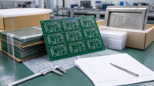
A 2.4GHz PCB antenna is commonly used in Wi-Fi, Bluetooth, Zigbee, IoT wireless modules, smart sensors, gateways, medical electronics, wearable devices, and compact connected products. It allows wireless communication without adding a separate external antenna, but it also makes the PCB layout and manufacturing process more sensitive.
For EBest Circuit (Best Technology), the focus is not to design the antenna from zero or replace the customer’s RF engineering work. Our role is to manufacture and assemble the PCB according to customer-approved design files, while helping review manufacturability risks around the antenna area, RF feed line, material, surface finish, impedance notes, SMT assembly, inspection, and testing requirements. If you are preparing a 2.4GHz PCB antenna board, send your Gerber files, ODB++ files, stackup, BOM, drawings, module datasheet, or assembly notes to sales@bestpcbs.com for engineering review before production.

What Is a 2.4GHz PCB Antenna?
A 2.4GHz PCB antenna is an antenna structure formed directly on the printed circuit board. Instead of using only an external antenna, the board itself includes a copper antenna pattern that operates around the 2.4GHz frequency band.
This frequency band is extensively used by:
- Wi-Fi
- Bluetooth
- BLE devices
- Zigbee
- Thread
- Some IoT wireless modules
- Smart home products
- Wireless sensors
- Compact industrial devices
The antenna may appear as a meandered trace, inverted-F antenna, chip antenna connection area, patch-style antenna structure, or another customer-defined antenna pattern. The exact antenna geometry should be defined and validated by the customer’s RF design team or module supplier. During PCB manufacturing, the board supplier must protect this geometry and avoid process changes that may affect performance.

How Does a 2.4GHz Antenna PCB Work?
A 2.4GHz antenna PCB works by using copper geometry on the PCB to radiate and receive electromagnetic signals. The antenna area, feed line, ground reference, keep-out zone, material, board thickness, nearby components, and enclosure can all affect wireless performance.
From a PCB manufacturing point of view, several areas matter:
| Area | Why It Matters |
|---|---|
| Antenna geometry | Must match customer-approved files |
| Keep-out area | Avoids unwanted copper or metal interference |
| RF feed line | May require impedance control |
| Ground reference | Supports stable RF behavior |
| Material | Affects dielectric properties |
| Surface finish | Affects soldering and long-term reliability |
| Assembly | Components near antenna may affect performance |
The PCB manufacturer should not casually modify the antenna trace, copper pour, ground clearance, or feed area. Even small changes may affect tuning, signal strength, or final wireless performance.
Common Types of 2.4GHz PCB Antennas
Different products may use different 2.4GHz PCB antenna styles. The choice is usually made by the customer’s RF engineer, wireless module supplier, or reference design provider.
Common types include:
Meandered PCB antenna
A compact trace antenna often used when board space is limited. It can be useful for Bluetooth, BLE, and small IoT devices.
Inverted-F antenna
A common PCB antenna type for 2.4GHz wireless products. It usually requires careful control of the antenna shape, feed point, ground, and keep-out area.
PCB patch antenna
A patch antenna structure may be used when the project needs a defined radiation direction or board-level antenna area.
Chip antenna with PCB matching area
Some products use a ceramic chip antenna or module antenna. Even in this case, the PCB layout around the chip antenna, ground clearance, feed line, and matching components still matters.
External antenna connector design
Some 2.4GHz products use an RF connector such as IPEX/U.FL or SMA. The PCB still needs proper RF feed line routing, connector footprint, soldering quality, and mechanical stability.
EBest Circuit manufactures the PCB or PCBA according to the customer-approved 2.4 GHz antenna PCB design, module supplier recommendations, Gerber files, stackup, and production notes.

2.4GHz PCB Antenna Design Files and Manufacturing Checks
The phrase 2.4GHz PCB antenna design can mean many things. For some engineers, it means antenna simulation and RF tuning. For a PCB manufacturer, the practical focus is different: whether the approved antenna design files can be manufactured and assembled without introducing avoidable risk.
Before production, EBest Circuit can help review:
- Gerber or ODB++ files
- Stackup and board thickness
- Material requirement
- Copper thickness
- Antenna keep-out area
- RF feed line notes
- Controlled impedance requirements
- Solder mask openings
- Surface finish
- Module footprint
- Connector footprint
- Panelization
- Test points and inspection notes
If the customer provides a wireless module datasheet or reference layout, it should be checked against the actual PCB files. This helps reduce mismatches between the intended RF layout and the board that will be produced.
2.4GHz WiFi PCB Antenna Layout Areas to Protect
A 2.4GHz WiFi PCB antenna is sensitive to its surrounding area. Even if the antenna pattern is correct, the final board may still perform poorly if the keep-out area, ground, enclosure, connector, or nearby components are not controlled.
Important areas to protect include:
| Area | Manufacturing Concern |
|---|---|
| Antenna copper | Do not change shape or length |
| Keep-out zone | Avoid copper, vias, or components |
| Feed line | Follow impedance and width notes |
| Ground clearance | Match approved layout |
| Matching circuit | Preserve pad and component positions |
| RF connector | Control soldering and alignment |
| Board edge | Avoid outline changes near antenna |
The PCB factory should not add copper balancing, tooling marks, vias, labels, or panel rails inside the antenna keep-out zone unless the customer confirms it. For antenna products, small “helpful” edits can become performance risks.
2.4GHz Patch Antenna PCB vs Meandered PCB Antenna
A 2.4GHz patch antenna PCB and a meandered PCB antenna serve different layout and product needs.
| Antenna Type | Typical Use |
|---|---|
| Patch antenna PCB | Larger antenna area, more directional behavior |
| Meandered PCB antenna | Compact products and space-saving layouts |
| Chip antenna layout | Small devices using supplier-defined antenna parts |
| External antenna connector | Products needing detachable or higher-gain antenna options |
For PCB manufacturing, the key is not to decide which antenna type is best. That decision belongs to the customer’s RF design team. The PCB manufacturer’s responsibility is to keep the approved antenna structure, material, copper, surface finish, and board outline consistent with the production files.
This is especially important for products such as IoT sensors, wireless gateways, Bluetooth devices, smart home controllers, medical wearables, and compact industrial modules.

PCB Material and Surface Finish for 2.4GHz PCB Antenna Boards
Many 2.4GHz PCB antenna boards are made with FR4, especially for common IoT, Bluetooth, Wi-Fi, and smart device products. However, material selection still matters because dielectric properties, board thickness, copper thickness, and stackup can affect RF behavior.
Common manufacturing points include:
- FR4 material grade
- Tg requirement
- Board thickness tolerance
- Copper thickness
- Solder mask type
- ENIG or other surface finish
- Controlled impedance requirement
- RF feed line geometry
- Consistent production stackup
ENIG is often selected when the project needs good solderability, flat pads, fine-pitch assembly, or better surface stability. For cost-sensitive products, other surface finishes may also be possible, but the choice should match the assembly process and product reliability requirements.
For high-volume or high-reliability wireless products, production consistency matters. A prototype that works well should not become unstable in batch production because of uncontrolled material or stackup changes.
PCBA Assembly Risks for 2.4GHz PCB Antenna Products
PCBA assembly can affect 2.4GHz PCB antenna products even when the bare PCB is correct. The module, RF connector, matching components, shield, crystal, sensor, power circuit, and nearby components must be assembled consistently.
Common PCBA risks include:
- RF connector misalignment
- Poor solder joints on module pads
- Wrong component value in matching circuit
- Residue near fine-pitch or RF areas
- Component shift near antenna keep-out zone
- Incorrect BOM substitution
- Shielding cover assembly issues
- Insufficient inspection around small passive components
- Testing notes missing from production files
EBest Circuit can support PCB SMT assembly, connector assembly, component sourcing based on approved BOM, AOI inspection, X-ray inspection when needed, functional testing coordination, and packing. For RF performance testing or wireless certification, the customer usually defines the test method or works with a dedicated RF test lab. EBest Circuit can coordinate production testing according to approved customer instructions.
2.4GHz PCB Antenna Board Manufacturing Case Study
A customer from Europe needed a small flexible PCB used in a compact 2.4GHz wireless product. The antenna-related structure and circuit files were already defined by the customer. EBest Circuit’s role was to manufacture the FPC according to the approved files and control the details that could affect assembly, connection reliability, and product fit.
Project requirements
- 2-layer FPC
- 0.5oz RA copper
- Finished thickness: 0.15mm
- Finger opening area: 0.30mm
- PI stiffener and FR4 stiffener
- Customer-approved antenna-related layout
- Flexible connection area for compact assembly
Why this project needed careful review
This project looked small, but it had several details that needed control. The 0.15mm FPC thickness affected flexibility and installation fit. The 0.5oz RA copper was important for bending reliability because rolled annealed copper is often preferred for flexible circuits that need better ductility.
The finger opening area also needed careful manufacturing control. If the opening was not accurate, it could affect contact reliability during assembly. The PI and FR4 stiffeners had to be placed correctly to support the connection area and protect the flexible section from unnecessary stress.
EBest Circuit’s manufacturing support
- Reviewed FPC files before production
- Confirmed 2-layer FPC structure and 0.15mm finished thickness
- Controlled 0.5oz RA copper requirements
- Checked finger opening area and stiffener position
- Manufactured PI and FR4 stiffener areas according to customer files
- Protected the approved antenna-related layout during production preparation
For the customer, the value was not antenna redesign. The value was precise FPC manufacturing. The board had to remain flexible where bending was needed, reinforced where connection support was required, and consistent with the customer-approved 2.4GHz wireless product files. This helped the customer move the compact wireless product toward assembly and validation with fewer manufacturing risks.

Why Choose EBest Circuit for 2.4GHz PCB Antenna PCB and PCBA?
EBest Circuit is suitable for customers who already have approved 2.4GHz PCB antenna design files and need reliable PCB manufacturing, component sourcing, PCBA assembly, and production support.
Customers choose EBest Circuit because we can support:
- PCB fabrication
- DFM review before production
- Stackup and material review
- Controlled impedance review when required
- ENIG and other surface finish options
- Component sourcing based on approved BOM
- SMT assembly
- Connector assembly
- AOI and inspection support
- Functional testing coordination
- Prototype and small-batch production
- One-stop PCB + sourcing + assembly service
For 2.4GHz antenna board projects, EBest Circuit pays special attention to antenna keep-out areas, RF feed line notes, module footprints, connector positions, surface finish, panelization, and assembly reliability. These details help reduce manufacturing risk without crossing into unsupported RF antenna design work.
If you are preparing a 2.4GHz PCB antenna board, send your Gerber files, ODB++ files, stackup, BOM, module datasheet, drawings, or assembly notes to sales@bestpcbs.com. Our engineering team can help review the PCB and PCBA manufacturing path before production starts.
FAQs about 2.4GHz PCB Antenna
1. What is a 2.4GHz PCB antenna?
A 2.4GHz PCB antenna is an antenna structure made from copper traces on the PCB. It is often used in Wi-Fi, Bluetooth, BLE, Zigbee, and IoT wireless products.
2. Can EBest Circuit design a 2.4GHz PCB antenna from zero?
EBest Circuit mainly supports PCB manufacturing, DFM review, component sourcing based on approved BOM, PCBA assembly, inspection, and testing coordination. We manufacture and assemble according to customer-approved antenna design files and production requirements.
3. Why is the antenna keep-out area important?
The antenna keep-out area helps prevent unwanted copper, vias, components, metal parts, or panel features from affecting wireless performance. It should follow the approved antenna layout or module supplier recommendation.
4. What surface finish is suitable for 2.4GHz PCB antenna boards?
ENIG is widely used when the project needs flat pads, good solderability, fine-pitch assembly, or reliable surface quality. The final choice should match the assembly and product requirements.
5. What files should I send for a 2.4GHz PCB antenna board project?
You can send Gerber or ODB++ files, stackup, BOM, drawings, module datasheet, antenna layout notes, impedance notes, placement file, assembly notes, and testing requirements.
Need help with a 2.4GHz PCB antenna board project? Pls feel free to send your Gerber files, ODB++ files, stackup, BOM, drawings, module datasheet, or assembly requirements to sales@bestpcbs.com. EBest Circuit’s engineering team can help review the PCB and PCBA manufacturing path before production.