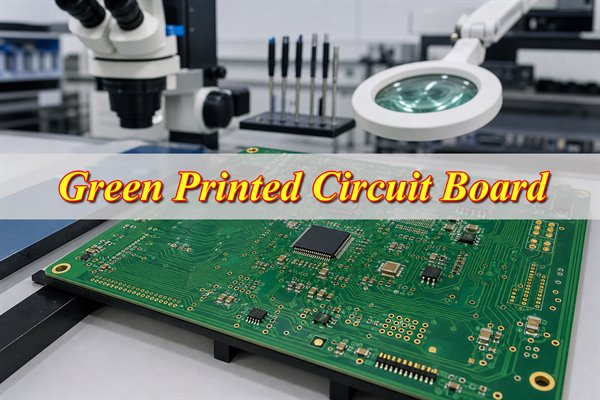
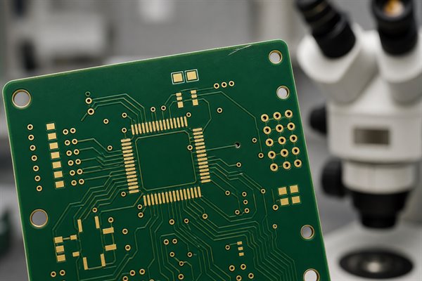
A green printed circuit board is a PCB whose outer copper circuitry is covered by green solder mask. The green layer is normally a protective polymer coating, not the structural laminate and not the copper itself.
Color is only the visible starting point. Designers and buyers must also specify the substrate, copper weight, stackup, mask system and clearances, surface finish, assembly scope, inspection criteria and operating environment. Together, these choices determine whether the board can be fabricated, assembled and inspected reliably.
What Is a Green Printed Circuit Board?
The green surface is solder mask. A green printed circuit board is a functional PCB finished with that protective coating on one or both outer surfaces. The mask covers most external copper while leaving component pads, test points, selected vias and contact areas open according to the fabrication data.
The phrase may refer to a bare board or an assembled board inside a product. The purchase specification must distinguish bare PCB fabrication from component assembly or turnkey PCBA service. Color does not define layer count, base material, copper thickness, surface finish or electrical performance.
Why Are Printed Circuit Boards Green?
Green became the practical production default. It provides good visual contrast against copper, pads, white legend and many surface finishes, which helps during manual inspection and process control.
Long-term use and process standardization reinforced that choice: fabricators process green mask routinely, and inspection teams know how it should look. Other colors are widely available, but green remains the default when appearance is not a product requirement. It is not inherently higher quality; quality depends on materials, artwork, process control and acceptance criteria.
Does the Green Color Come from the PCB Material or Solder Mask?
The pigment is in the solder mask. The visible green color normally does not come from the PCB core material. FR-4 laminate is typically a translucent tan or yellowish composite of woven glass reinforcement and cured epoxy resin. Copper is reddish metallic before processing, while common surface finishes create tin, silver or gold-colored exposed pads.
| Visible feature | Typical material or process | What it controls |
| Green surface | Pigmented solder mask | Copper protection, solder control and surface identification |
| Board structure | FR-4 or another specified laminate | Mechanical support, insulation, thermal and electrical behavior |
| Conductive pattern | Copper foil and plated copper | Power and signal interconnection |
| Exposed pads | HASL, ENIG, OSP or another finish | Solderability, contact surface and storage considerations |
| White markings | Legend or silkscreen ink | Reference designators, polarity and assembly information |
What Are Green Circuit Boards Made Of?
A green PCB is built from several bonded materials. Its structure normally includes an insulating laminate, copper conductors, resin-rich bonding layers, plated holes, solder mask, a finish on exposed pads and legend ink. The visible green surface is only the outer coating; it does not identify every material inside the board.
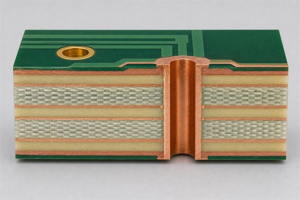
- Core laminate: Standard rigid boards commonly use FR-4, cured epoxy resin reinforced with woven glass cloth. It provides insulation, mechanical strength and a stable base for copper. High-Tg FR-4 may be selected for higher assembly or operating temperatures.
- Copper foil: Electrodeposited or rolled copper forms traces, power areas, pads and internal planes. State both base and finished copper requirements; green color reveals nothing about conductor thickness or current capacity.
- Prepreg bonding layers: Multilayer PCBs use sheets of glass cloth impregnated with partially cured resin between cores. During lamination, heat and pressure make the resin flow and cure, bonding the copper-patterned layers into one structure.
- Plated-hole metal: Copper is deposited and electroplated onto drilled hole walls to connect layers. Depending on the finish and process, exposed hole or pad surfaces may also contain nickel, gold, tin, silver or solder.
- Green solder mask: This pigmented polymer coating covers most external copper, defines openings around pads and test points, limits solder spread and protects conductors from contamination and oxidation.
- Surface finish: Exposed copper pads require a solderable protective finish such as HASL, ENIG, OSP, immersion silver or immersion tin. The finish is chosen for assembly method, pad geometry, storage conditions, contact requirements and customer specifications.
- Legend ink: White or another contrasting epoxy-based ink prints component references, polarity marks and assembly information over the cured mask. Legend ink is an identification layer and should not overlap solderable pads.
- Optional functional materials: A design may add via-fill resin, conductive paste, peelable mask, carbon ink, embedded copper, aluminum or copper metal cores, ceramic substrates, polyimide flex layers or specialized low-loss laminates. These materials must be defined separately from the green solder mask.
Green vs Blue vs Brown PCB: What Is the Difference?
Color does not define circuit function. Green, blue and brown boards differ mainly in visible coating or substrate appearance. Green and blue normally refer to solder mask pigments. A brown board may use brown solder mask, but it can also expose a brown phenolic-paper laminate, so its base material must be confirmed before comparing performance.
| Comparison point | Green PCB | Blue PCB | Brown PCB |
| What creates the color | Usually green solder mask over FR-4 or another specified substrate | Usually blue solder mask over the same range of possible substrates | Brown solder mask or a visible brown phenolic-paper laminate; verify which one applies |
| Manufacturing availability | Most established default and normally the easiest color to source consistently | Commonly available, but shade and process capability should be confirmed | Less standardized; availability depends on whether brown means mask color or laminate type |
| Inspection contrast | Strong contrast with copper, gold-colored pads and white legend; familiar for manual inspection and AOI setup | Good contrast with white legend and metallic pads, although trace visibility and shade vary by ink | Darker backgrounds can reduce visual contrast; exposed phenolic material may also show more color variation |
| Fine-feature decisions | Often the baseline process for reviewing small mask dams and tight registration | Use the blue ink supplier’s qualified minimum dam, registration and cure window | Do not infer capability from color; confirm the actual mask system or phenolic-board process |
| Electrical and thermal behavior | Controlled mainly by substrate, copper geometry and the selected mask formulation | Comparable when construction and qualified mask properties are equivalent | May differ significantly if the board uses phenolic paper instead of FR-4; material designation is essential |
| Best reason to choose it | Standard production, inspection familiarity and broad availability | Product identification or a required visual design without changing the PCB construction | Legacy appearance, product identification or a cost-driven phenolic construction where technically suitable |
If the same FR-4 stackup, copper, surface finish and qualified solder mask system are used, changing green to blue or brown does not automatically improve electrical performance. The procurement drawing should name both the solder mask color and the substrate material so a cosmetic request cannot be mistaken for a material substitution.
What Design Rules Matter for a Green Circuit Board?
Mask geometry must be designed deliberately. Control openings, dams, registration and interaction with pads, vias and test points. The correct values come from the selected fabrication process rather than from a universal online rule.
- Pad clearance: Define solder mask expansion so registration tolerance does not cover the intended solderable area.
- Mask dams: Review narrow mask webs between fine-pitch pads with the manufacturer before release.
- Via treatment: State whether vias are open, tented, plugged, filled or capped; do not rely on missing artwork to communicate intent.
- Fiducials: Keep the required copper and mask clearance around local and global fiducials for reliable machine vision.
- Test access: Ensure probes contact exposed, finished test pads rather than mask-covered copper.
- High-copper areas: Consider coating uniformity and edge coverage where copper height changes abruptly.
- RF features: Define mask coverage or keepout deliberately for controlled-impedance lines and antennas.
- Legend placement: Keep markings away from pads and exposed contacts to avoid assembly ambiguity.
How Is a Green Printed Circuit Board Manufactured?
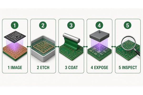
Green mask is one stage in the full PCB process. For a multilayer board, production runs from engineering data review through inner-layer imaging, lamination, drilling, copper plating, outer-layer patterning, solder mask, surface finish, profiling, electrical test and final inspection.
- Engineering and DFM review: Gerber or ODB++, NC drill, stackup, impedance data, mask layers, dimensions and fabrication notes are checked for missing data and conflicts.
- Material preparation: Copper-clad cores and prepreg are selected to the approved material specification, cut into production panels and identified for traceability.
- Inner-layer imaging: Photoresist is applied to multilayer cores, exposed with the inner circuit image and developed to define the protected copper pattern.
- Inner-layer etching and AOI: Unwanted copper is etched away. Automated optical inspection checks opens, shorts, spacing and image defects before the layers are buried.
- Oxide treatment and layup: Inner copper surfaces are prepared for bonding. Cores, prepreg and outer copper foils are stacked in the required sequence.
- Lamination: Controlled heat, pressure and vacuum cure the prepreg resin and bond the multilayer package into a rigid panel.
- Drilling: CNC drilling or laser processing creates component holes, vias, tooling holes and, where required, microvias according to the drill data.
- Desmear and electroless copper: Resin residue is removed from drilled hole walls, and a thin conductive copper layer is deposited to prepare the holes for electroplating.
- Outer-layer imaging and pattern plating: The external circuit image is developed, then copper is electroplated onto traces and through-hole walls. A temporary etch resist protects the required circuitry.
- Outer-layer etching and AOI: Unwanted external copper is removed, the resist is stripped and the finished outer circuitry is optically inspected.
- Solder mask surface preparation: Copper and laminate surfaces are cleaned and micro-roughened so the green coating can adhere without contamination or trapped moisture.
- Green mask coating and pre-dry: LPI material is screen coated, sprayed or curtain coated to the qualified wet-film build, then partially dried for imaging.
- Exposure and development: UV or direct imaging hardens the required mask areas. Developer removes mask from pads, selected vias, test points and other specified openings.
- Final mask cure: Thermal and, where applicable, UV curing complete the polymer reaction and establish adhesion, hardness, chemical resistance and solder-process durability.
- Surface finish and legend: Exposed pads receive the specified finish, such as HASL, ENIG or OSP, in the approved process sequence. Legend ink adds reference designators and assembly markings.
- Profiling and edge work: Routing, V-scoring, beveling, castellations or other specified mechanical processes form the final board outline and features.
- Electrical test: Flying-probe or fixture testing checks continuity and isolation against the netlist. Controlled-impedance orders may also require coupon measurement.
- Final inspection and packaging: Dimensions, holes, surface finish, solder mask registration, cosmetic condition and documentation are checked before cleaning, vacuum packing and shipment preparation.
What Common Green Solder Mask Defects Should Be Checked?
Mask defects can become assembly defects. Inspection should find conditions that expose copper, cover solderable areas, weaken insulation or create soldering risk. Acceptance depends on the board class, drawing, customer criteria and applicable workmanship standard.
- Misregistration: Mask shifts toward or onto pads and reduces usable solderable area.
- Missing mask: Unintended exposed copper can oxidize or create solder-bridging risk.
- Mask on pads: Residue or partial coverage can reduce solder wetting and joint area.
- Pinholes and voids: Small discontinuities may expose copper or indicate coating-process instability.
- Scratches and damage: Handling or routing can break the cured coating after imaging.
- Blisters or delamination: Poor adhesion, contamination, moisture or cure problems can lift the mask.
- Uneven cure or color: Appearance variation should trigger process review when it correlates with adhesion or coating differences.
- Blocked vias or holes: Unplanned mask intrusion can interfere with assembly, test or mechanical fit.
What Green PCB Manufacturing and Assembly Services Can We Provide?
EBest provides five services for custom green PCB projects. Each can be ordered separately or combined into one design-to-assembly program.
- PCB design: Engineering support reviews board structure, copper requirements, mask openings, via treatment, component placement and manufacturability before release, exposing avoidable fabrication and assembly risks early.
- PCB prototyping: Prototypes verify dimensions, interfaces, stackup, mask registration and assembly fit before higher-volume production.
- Mass production: EBest supports repeat green PCB manufacturing after the design, materials and acceptance requirements are approved. The product portfolio includes FR-4, single-sided, multilayer, metal-core, ceramic, semi-rigid-flex, RF, high-Tg, heavy-copper, HDI, extra-thin, busbar, IC-substrate, high-speed and impedance-control PCBs.
- Component sourcing: Sourcing follows the approved BOM. Manufacturer part numbers, permitted alternates and lifecycle constraints prevent purchasing changes from altering form, fit or function.
- PCB assembly: Bare-board fabrication can be combined with placement and the agreed programming, inspection and testing scope. One coordinated path reduces mismatches among board data, footprints, the BOM and assembly instructions.
For an actionable review, provide Gerber or ODB++, NC drill, stackup, board thickness, copper weight, surface finish, green solder mask requirements, quantity and inspection criteria. For assembly, also send the BOM, centroid file, assembly drawings, approved substitutions, programming instructions, test method and required quality documents.
Custom Green PCB Manufacturing and Assembly Case Study
One-stop production matters when PCB and assembly data interact. This representative industrial-controller project shows how a single review path turns separate design files into one controlled manufacturing package.
Project Background: The controller combined digital control, analog sensing and power circuitry on a compact multilayer green PCB. The buyer needed bare-board fabrication, component sourcing and assembly from one supplier, but also needed approved parts, programming access and test points to remain under revision control.
Project Requirements: The quotation package included Gerber/ODB++, NC drill, stackup, BOM, centroid data and assembly drawings. The engineering review had to confirm copper requirements, green mask openings, via treatment, fiducials, polarity marks, programming connections and test access. Fine-pitch pads also required a manufacturable solder mask dam instead of relying only on the nominal CAD opening.
Our Solution: EBest cross-checked the fabrication, drill, stackup, BOM and placement files before release. Mask expansion and minimum dams were reviewed against production capability; via treatment was clarified near solderable pads; fiducials, thermal copper transitions, polarity marks and probe access were checked for assembly and test. Manufacturer part numbers and approved alternates were then frozen with the assembly package so purchasing could not silently change fit or function.
Output Results: Before production, the buyer received one consolidated set of engineering questions and an approved revision package rather than separate interpretations from a board shop, component buyer and assembler. The agreed deliverables comprised fabricated boards, assembled units and the specified inspection or test records. For repeat orders, the approved material, BOM, fabrication notes and acceptance criteria provided a clear change-control baseline, reducing the risk of an unreviewed change between prototype and volume production.
What Specifications Affect Green PCB Cost and Lead Time?
Color is only one quotation input. Board construction, feature difficulty, material availability, test scope and assembly content usually have greater impact on quotation and schedule. A complete data package helps the manufacturer identify risk early and avoid repeated clarification.
- Board construction: Layer count, finished thickness, panel utilization and material family affect process routing.
- Copper and features: Copper weight, minimum trace and space, hole sizes, aspect ratio and HDI structures affect difficulty.
- Solder mask demand: Very narrow dams, tight registration, unusual thickness requirements or special-property ink require review.
- Surface finish: Finish selection changes processing, material use, shelf-life planning and inspection.
- Mechanical work: Controlled depth, countersinks, edge plating, castellations and tight outline tolerances add operations.
- Quality scope: Coupon testing, impedance reporting, microsections, special documentation and additional inspection add work.
- Assembly content: BOM availability, package mix, fine pitch, bottom-terminated components, programming and functional test affect PCBA planning.
- Order conditions: Quantity, panel strategy, approved alternates and requested schedule influence material and production decisions.
Why Choose EBest Circuit as Your Green PCB Manufacturer?
A supplier should reduce risk before production starts. EBest Circuit connects engineering review, fabrication, component sourcing and assembly so design decisions remain consistent from quotation through delivery.
- Catch costly issues before fabrication: Engineering review checks stackup, copper requirements, solder mask openings, via treatment, manufacturability and assembly inputs before release. Earlier clarification lowers the risk of board respins, quotation changes and production holds.
- Match the board construction to the application: FR-4, metal-core, ceramic, flex-related, RF, high-Tg, heavy-copper, HDI, high-speed and impedance-control options allow material and structure to follow electrical, thermal and mechanical needs instead of forcing one standard build.
- Keep one accountable project path: Design support, prototyping, mass production, sourcing and assembly can be coordinated under one approved package. This reduces responsibility gaps when a stackup, footprint, BOM or test issue crosses production stages.
- Protect BOM and assembly intent: Component sourcing follows manufacturer part numbers, approved alternates and lifecycle constraints. Coordinating the BOM with board data and placement files reduces the chance of substitutions, footprint mismatches or missing assembly instructions.
- Carry approved data from prototype to volume: Prototype findings, material choices, fabrication notes and acceptance criteria can remain tied to the same project package during repeat production. That continuity reduces avoidable changes between sample approval and recurring orders.
- Protect urgent schedules with confirmed options: Eligible boards may ship in as little as 24 hours after engineering, material and process confirmation. The commitment is checked against board complexity and current production status, giving buyers a usable schedule rather than an unconditional speed claim.
- Request quality evidence that fits the order: EBest lists IATF 16949, ISO 9001:2015, ISO 13485:2016, AS9100D, REACH, RoHS and UL. Buyers can request the applicable certificate, material recognition, declaration, inspection record or test report instead of assuming one credential covers every product.
FAQs About Green Printed Circuit Boards
Q1: Can the green shade be kept consistent across repeat orders?
A1: Specify the approved mask system and color reference. Shade consistency can be controlled more effectively when the drawing identifies the approved solder mask manufacturer, product code, finish and reference sample. Different ink lots, copper patterns and coating builds can still create small visual differences. If appearance matters to the finished product, agree on an acceptable color range or signed sample before mass production.
Q2: Should a green PCB use a glossy or matte solder mask?
A2: Choose gloss level according to inspection and appearance needs. Glossy mask can give a brighter, more reflective surface, while matte mask can reduce glare during handling or photography. Gloss level is a material-system choice, not merely a cosmetic after-treatment, so specify it before the fabricator selects the ink.
Q3: How should bare green PCBs be stored before assembly?
A3: Keep boards sealed, clean and dry. Protect exposed finishes from moisture, sulfur, fingerprints and abrasion. Follow the storage period and bake guidance for the selected surface finish and laminate. If packaging is opened or storage limits are exceeded, review solderability and moisture condition before assembly instead of relying on appearance alone.
Q4: Can conformal coating be applied over green solder mask?
A4: Yes, when the materials and cleanliness level are compatible. Flux residue, silicone, oil or insufficient mask cure can reduce coating adhesion. Define keepout areas around connectors, switches, test points and heat sinks, then validate adhesion and cure on the actual material combination used for production.
Q5: Can a scratched green solder mask be repaired?
A5: Minor damage may be repairable under an approved procedure. Repair is not automatically acceptable for every class, location or customer. Damage near fine-pitch pads, high-voltage spacing, RF features or exposed copper should be evaluated against the drawing and acceptance requirements.
Q6: Does the solder mask lot need traceability?
A6: Track the mask lot when qualification matters. The record may include manufacturer, product code, lot number, mixing date, shelf-life status and cure record. Define the needed evidence in the purchase documentation so it is captured during production rather than reconstructed afterward.
Q7: Should production coupons receive the same green solder mask?
A7: Match the production mask for representative coupons. Some electrical coupons are designed for measurements before or without mask, so the correct construction depends on the test purpose. State the coupon construction and measurement stage in the stackup or fabrication notes.
Q8: Can green solder mask be laser marked?
A8: Some mask systems can be laser marked after process validation. Contrast, readability and coating damage depend on wavelength, energy and ink formulation. Run a material trial before using laser marks for serial numbers or traceability. The process must not expose copper, reduce required insulation or make identification unreadable after assembly.
Q9: How should cosmetic acceptance be defined for visible green PCBs?
A9: Define cosmetic limits before production. If the board remains visible in the final product, specify allowable shade variation, scratches, stains, gloss differences, repair marks and legend quality. Use an approved sample or documented limit where appearance is critical. Standard electrical acceptance alone may not resolve a disagreement about customer-facing cosmetic expectations.
Q10: What should be checked when changing to a different green solder mask supplier?
A10: Requalify the material and process before approving the change. Recheck color, adhesion, cure window, solder resistance, chemical compatibility, dielectric properties, minimum feature capability and applicable recognition. For sensitive products, use controlled trial panels and the required qualification evidence. A visually similar green ink should not be assumed to be technically interchangeable.
Conclusion
Define the complete board, not only its green color. Substrate, stackup, copper, solder mask type and thickness, openings, via treatment, surface finish, inspection level and assembly scope determine whether the finished green printed circuit board will meet the project requirement.
Send your Gerber/ODB++, NC drill, stackup and BOM, together with quantity, assembly files, target schedule and test requirements, to sales@bestpcbs.com. EBest’s engineering team can review manufacturability, identify missing quotation inputs and prepare a clearer PCB or turnkey PCBA quotation. Submit your files today so technical risks can be resolved before they become production delays or redesign costs.