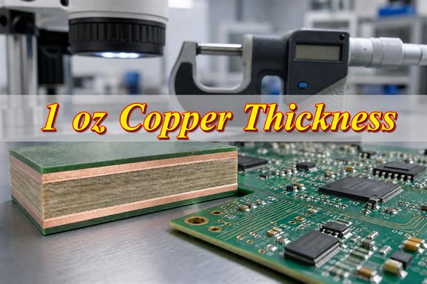
1 oz copper thickness is nominally about 34.8 microns. That equals approximately 0.0348 mm, 1.37 mils, or 0.00137 inches. The term does not mean that a finished circuit trace contains one ounce of copper. It describes the mass of copper distributed over one square foot, which fabricators convert into a nominal foil thickness.
This guide is for PCB designers, hardware engineers, sourcing teams, quality engineers, and buyers who need to interpret a stackup or fabrication drawing. It explains why a finished board may not measure exactly 35 µm, how inner and outer layers differ, and how to specify copper so the manufacturer understands the electrical and manufacturing requirement.
What Does 1 oz Copper Thickness Mean in PCB Manufacturing?
It means one ounce of copper per square foot. Its nominal thickness is approximately 34.8 µm, commonly rounded to 35 µm. The designation is a copper weight per unit area, not the mass of copper on an individual board.
The same copper-weight label can describe laminate foil before processing or the target copper on a finished layer. Those are not always equivalent. Cleaning and etching remove copper from inner layers, while electroplating normally adds copper to outer-layer conductors and plated-hole walls. A drawing that says only “1 oz copper” can therefore leave room for different interpretations.
- Nominal conversion: The PCB industry commonly associates the 1 oz/ft² class with about 34.8 µm.
- Common shorthand: Suppliers often state 35 µm or 1.4 mil for convenience.
- Manufacturing meaning: Confirm whether the value refers to starting foil or finished conductor copper.
- Layer requirement: Inner and outer layers may need separate copper specifications.
How Thick Is 1 oz Copper in mm, Microns, Mils and Inches?
The nominal thickness is 34.8 µm. This converts to 0.0348 mm, 1.37 mils, or 0.00137 inches. Many drawings round these figures to 0.035 mm, 35 µm, 1.4 mils, and 0.0014 inches. Both sets describe the same nominal copper-weight class. For critical electrical, thermal, or impedance calculations, use the fabricator-confirmed finished conductor thickness instead of a generic conversion.
| Unit | Nominal Value | Common Drawing Value |
| Millimeters | 0.0348 mm | 0.035 mm |
| Microns | 34.8 µm | 35 µm |
| Mils | 1.37 mil | 1.4 mil |
| Inches | 0.00137 in | 0.0014 in |
These are nominal industry conversions, not a promise that every point on a processed PCB will have exactly that thickness. Copper-foil tolerance, micro-etching, pattern plating, copper distribution, and the applicable acceptance class all affect the finished result.
Why Is PCB Copper Thickness Measured in Ounces?
The ounce denotes copper mass over a standard area. One ounce per square foot can be converted into thickness because copper density is known. Weight-per-area measurement also represents the average foil more reliably than a single contact measurement on a microscopically rough surface.
The complete unit is oz/ft², although PCB quotations and fabrication notes usually shorten it to oz. This convention remains useful for ordering common foil classes such as 0.5 oz, 1 oz, and 2 oz. Engineers still convert the weight into microns or mils for impedance models, current-capacity calculations, mechanical stackups, and tolerance reviews.
How Is the Thickness of 1 oz Copper Calculated?
Thickness equals copper volume divided by area. Using 28.35 grams for one avoirdupois ounce, a copper density of 8.96 g/cm³, and an area of 929.03 cm² gives an ideal mathematical thickness of about 0.003406 cm, or 34.06 µm. PCB fabrication references commonly use the nominal industry conversion of approximately 34.8 µm, 1.37 mils, or 0.0348 mm for the 1 oz copper class. These values describe a nominal weight class, not a finished-conductor acceptance limit.
The calculation assumes a uniform solid sheet and does not include manufacturing loss or plating buildup. It is therefore a reference conversion for copper weight 1 oz thickness, not a finished-board inspection limit. Acceptance should be based on the purchase specification, drawing notes, applicable IPC requirements, and the fabricator’s confirmed process capability.
What Is the Difference Between 1 oz Base Copper and Finished Copper Thickness?
Base copper is measured before circuit processing. Finished copper is the conductor thickness after etching, cleaning, and any required plating. A 1 oz base foil begins near the nominal 35 µm class, but an inner layer may finish thinner after processing. An outer layer may begin with lighter foil and finish near or above the target after pattern plating.
| Term | Production Stage | Design Implication |
| Nominal copper weight | Industry weight class | Useful for general stackup descriptions |
| Base or start copper | Foil before imaging and etching | Controls etching difficulty and achievable spacing |
| Finished inner copper | After cleaning and etching | May be lower than nominal start foil |
| Finished outer copper | After pattern plating and processing | Includes plated copper and varies across the panel |
This distinction explains why “PCB finished copper thickness 1 oz” must be discussed with the supplier instead of inferred from a laminate label. When a minimum conductor thickness matters, state the minimum finished value and the applicable layer rather than relying only on an ounce designation.
How Do Etching and Plating Affect 1 oz Finished Copper Thickness?
Etching removes copper; electroplating adds it. Inner-layer traces are normally imaged and etched from copper-clad laminate, so cleaning and micro-etch steps can reduce the final thickness. Outer layers on plated-through-hole boards receive additional copper during pattern plating before the unwanted copper is etched away.
Thicker starting copper requires more lateral etching to clear spaces between tracks. This can limit fine-line capability and require larger conductor spacing. Plating is also affected by feature density and current distribution across the production panel, so isolated features and dense copper areas may not build at identical rates.
- Micro-etch loss: Surface preparation removes a controlled amount of copper before bonding or plating.
- Pattern plating: Added copper increases outer conductor and hole-wall thickness.
- Etch compensation: Trace artwork may be adjusted to achieve the required finished width.
- Copper balance: More uniform distribution supports more consistent plating and dimensional stability.
Why Can 1 oz Copper Thickness Differ Between Inner and Outer PCB Layers?
Inner and outer layers follow different production routes. Their final copper thickness can therefore differ even when a stackup uses the same nominal designation. Inner copper is usually defined mainly by the starting foil minus process reduction. Outer copper combines the starting foil with electrodeposited copper required for conductive hole walls and outer-layer circuitry.
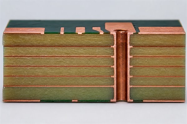
Layer position also changes thermal behavior. External traces release heat more effectively than internal traces surrounded by dielectric material. As a result, two traces with the same width and nominal copper thickness may not carry the same current at the same permitted temperature rise. Current calculations must identify whether the trace is internal or external.
For multilayer construction, copper weight should also be reviewed as part of a balanced stackup. Using substantially different copper construction on opposing sides can complicate etching and increase mechanical imbalance. Confirm asymmetric requirements with the fabricator before releasing production data.
How Does 1 oz Copper Thickness Affect PCB Trace Current Capacity?
Copper thickness alone does not determine allowable current. One-ounce copper contributes to the trace cross-sectional area, but trace width, length, layer position, permitted temperature rise, nearby heat sources, airflow, copper planes, via transitions, and laminate temperature limits must also be considered.
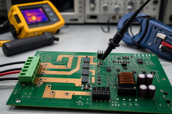
A wider 1 oz trace can often carry the required current without moving to 2 oz copper, and widening a trace may cost less than changing the entire board construction. However, space-constrained power paths, low-voltage high-current rails, motor controls, battery systems, and power converters may benefit from heavier copper after thermal analysis.
- Use the finished value: Calculate with the minimum finished conductor thickness, not an optimistic nominal figure.
- Separate layer conditions: Apply the correct internal or external conductor model.
- Check temperature rise: Select an allowable rise that fits components, laminate, enclosure, and reliability targets.
- Review bottlenecks: Pads, neck-downs, vias, connectors, and thermal reliefs may limit current before the main trace does.
- Validate critical paths: Use current-density and thermal simulation or representative testing for high-power designs.
1 oz vs 0.5 oz vs 2 oz Copper Thickness: What Is the Difference?
The main difference is conductor cross-section. Nominally, 0.5 oz is about 17.4 µm, 1 oz about 34.8 µm, and 2 oz about 69.6 µm. Increasing copper weight can reduce resistance for an unchanged trace width, but it also makes fine features harder to etch and can increase material, processing, and inspection requirements.
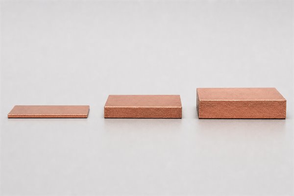
| Copper Weight | Nominal Thickness | Typical Fit | Design Trade-off |
| 0.5 oz | 17.4 µm / 0.69 mil | Fine features, multilayer inner layers, lower-current circuits | Less conductor area and lower damage margin |
| 1 oz | 34.8 µm / 1.37 mil | General digital, analog, control, and moderate-power boards | Balanced cost, availability, and routing capability |
| 2 oz | 69.6 µm / 2.74 mil | Higher-current rails, power conversion, industrial controls | Larger spacing, harder etching, and higher cost |
The comparison should be made with confirmed finished copper, not weight labels alone. For example, an outer layer that starts with lighter foil may be plated to a specified finished value. Ask the manufacturer for the proposed stackup and minimum finished thickness before final impedance or thermal sign-off.
When Should You Use 1 oz Copper Thickness for a PCB?
Use 1 oz copper when standard geometry meets the design limits. Check current, temperature rise, routing density, impedance, and manufacturing cost. It is a practical starting point for many general-purpose rigid PCBs because materials and fabrication processes are widely available.
- General control electronics: Logic, sensors, communication, and mixed-signal circuits commonly fit 1 oz construction.
- Moderate current: Wider traces or local copper pours can provide adequate conductor area without converting every layer to heavy copper.
- Dense routing: One-ounce copper generally supports finer features than 2 oz construction, subject to factory capability.
- Controlled impedance: It can be modeled reliably when the finished copper and dielectric geometry are confirmed.
- Cost-sensitive production: Standard constructions normally have broader supplier availability than unusual mixed-weight stackups.
Do not choose it only because it is a common default. Reconsider copper weight when current paths cannot be widened, voltage drop is excessive, thermal margins are narrow, mechanical wear is expected, or the finished-conductor minimum is controlled by a product standard. In those cases, compare heavier copper with alternative routing, busbars, multiple layers, or local reinforcement.
How Should 1 oz Copper Thickness Be Specified in PCB Manufacturing Files?
Specify the copper requirement for every layer. State whether each value is starting copper, nominal copper weight, or minimum finished conductor thickness. Place the requirement in the fabrication drawing and stackup, then keep it consistent with the Gerber or ODB++ data, impedance table, current calculations, and purchase order.
- Layer stackup: List the intended copper weight or thickness for every signal and plane layer.
- Finished requirement: State a minimum finished value when electrical or reliability calculations depend on it.
- Layer distinction: Separate inner-layer and outer-layer requirements instead of using one ambiguous global note.
- Acceptance basis: Identify the applicable drawing revision, product class, inspection requirement, and agreed standard.
- Impedance data: Provide target impedance, tolerance, referenced layers, and relevant line geometry.
- Fabricator review: Request a proposed stackup and capability confirmation before production release.
A useful note might state “35 µm nominal inner-layer copper; outer layers to meet the agreed minimum finished conductor thickness after plating.” The exact wording and values must match the design requirement and the selected fabricator’s process. Avoid copying a generic note without checking what its terms mean.
Why Choose EBest Circuit for 1 oz Copper PCB Manufacturing?
EBest Circuit reviews copper requirements as part of the PCB stackup. As a China-based PCB manufacturer serving global projects, the team can review layer-specific copper notes, routing constraints, impedance information, and production files for prototypes and volume production.
Before quotation, provide Gerber or ODB++, NC drill files, the stackup, finished board thickness, copper requirement by layer, surface finish, quantity, impedance targets, and any minimum finished-conductor requirement. For assembled products, also include the BOM, placement data, programming needs, test requirements, and quality documentation.
The most useful supplier response should confirm what “1 oz” means in the proposed construction, identify any line-width or spacing conflict, and return questions before material release. Contact the engineering team at sales@bestpcbs.com to review the project files and request a manufacturing quotation.
FAQs About 1 oz Copper Thickness
Q1: Is 1 oz copper exactly 35 microns thick?
A1: No. The industry nominal conversion is about 34.8 µm, commonly rounded to 35 µm. A strict mass-density calculation using the constants stated in this article gives about 34.06 µm, while actual finished thickness also varies with foil tolerance, inner-layer processing, and outer-layer plating. Use the agreed minimum finished thickness for acceptance or critical calculations.
Q2: Does the copper thickness include solder mask?
A2: No. Copper thickness describes the metallic conductor, while solder mask is a separate polymer coating applied over selected board areas. Surface finish is also specified separately. Inspection and electrical calculations should not add solder-mask thickness to the copper value.
Q3: Does ENIG or another surface finish increase copper thickness?
A3: A surface finish adds a separate metallic coating over exposed copper, but it is not normally counted as PCB copper weight. ENIG, immersion silver, OSP, HASL, and other finishes have different structures and thickness controls. Keep conductor copper and surface-finish requirements separate in the fabrication drawing.
Q4: Is 1 oz copper thick enough for a power PCB?
A4: It can be, but the answer depends on current, trace width, layer position, temperature rise, airflow, and voltage-drop limits. A wide 1 oz trace may outperform a narrow 2 oz trace. Check neck-downs, vias, connectors, and thermal reliefs because they often create the actual bottleneck.
Q5: Does 1 oz copper mean every PCB layer uses 1 oz?
A5: Not automatically. A stackup may combine different copper weights, such as lighter inner layers and heavier outer layers. If the fabrication drawing gives one global value, the manufacturer may apply a standard interpretation. List copper by layer to remove ambiguity.
Q6: How is finished PCB copper thickness verified?
A6: For critical requirements, the fabricator can verify conductor thickness through a prepared microsection and calibrated measurement. The inspection plan should identify the sampled location, layer, acceptance criterion, and applicable drawing or product standard. Surface measurements alone may not represent internal copper or plated-hole geometry.
Q7: Does heavier copper always carry twice the current?
A7: No. Doubling copper thickness doubles cross-sectional area only when trace width is unchanged, but allowable current is also limited by temperature rise, cooling, layer location, nearby heat sources, and connection geometry. The current rating therefore does not increase through a universal two-times rule.
Q8: Does 1 oz copper affect controlled impedance?
A8: Yes. Copper thickness changes conductor geometry, while plating can also change outer trace width and profile. The impedance model should use the manufacturer’s proposed finished geometry, dielectric thickness, and material properties rather than a generic 35 µm assumption.
Q9: What tolerance should be used for 1 oz copper?
A9: There is no safe universal percentage for every finished layer. Base-foil tolerance and finished-conductor acceptance depend on the material specification, process, product class, and purchase agreement. Specify the required minimum finished thickness and confirm the inspection basis with the fabricator.
Q10: What should a buyer confirm before ordering a 1 oz PCB?
A10: Confirm whether 1 oz refers to base or finished copper, which layers it applies to, the minimum finished requirement, line width and spacing capability, impedance construction, board thickness, surface finish, inspection class, and any current or thermal constraint. Keep the quotation, drawing, stackup, and purchase order consistent.
Conclusion
The finished PCB value depends on the manufacturing route. The nominal 1 oz copper thickness class is commonly stated as 0.0348 mm, 34.8 µm, 1.37 mils, or 0.00137 inches. Treat that industry conversion as a starting point, then distinguish base foil from finished inner and outer copper. Use the minimum finished conductor thickness for critical electrical, thermal, impedance, or acceptance decisions.
For an accurate quotation, submit the Gerber/ODB++, NC drill, stackup, and copper requirements, plus board thickness, surface finish, quantity, and impedance requirements. Send the package to sales@bestpcbs.com for an engineering review and manufacturing quotation.