PCB manufacturing PCB manufacturing
Home > Blog

PCB microsection

PCB Resin Recession: Identification, Causes, and Prevention
Saturday, September 5th, 2026
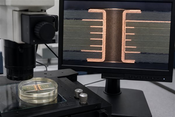
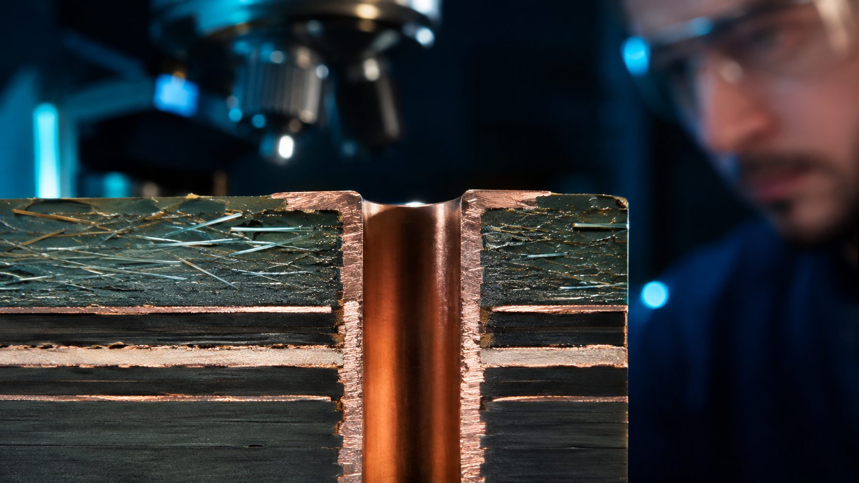
PCB microsection showing resin recessed beside a plated through-hole barrel
Resin recession is interpreted from the resin, glass and copper geometry in a controlled PCB cross-section.

PCB resin recession is a cross-sectional condition in which resin has receded from its expected boundary around a drilled or plated feature, leaving glass bundles or adjacent structures comparatively exposed. It is not automatically the same as copper-to-hole-wall pullaway, resin smear or a lamination void.

The practical question is not simply whether one dark or recessed area appears in a micrograph. Engineers must confirm the morphology, preparation quality, extent, test history and applicable acceptance criteria before assigning a root cause or lot disposition. A defensible investigation separates observation from interpretation and interpretation from corrective action.

What PCB Resin Recession Looks Like

In a prepared microsection, resin recession appears as resin pulled back or missing relative to nearby glass reinforcement, copper or the intended laminate boundary. The feature may be local around a hole wall or visible near internal-layer edges. Its shape and position should be documented across the entire section, not inferred from a tightly cropped image.

Look for exposed glass ends, a recessed resin boundary and whether the copper barrel remains intact and supported. Record the layer, quadrant, depth and length of the indication. Compare more than one hole and, when possible, compare suspect material with a known-good construction prepared by the same method.

Polishing relief can imitate recession. Soft resin and hard glass or copper remove at different rates during specimen preparation. If the indication changes substantially with preparation technique or appears only at a poorly supported edge, repeat the section before treating it as a production defect.

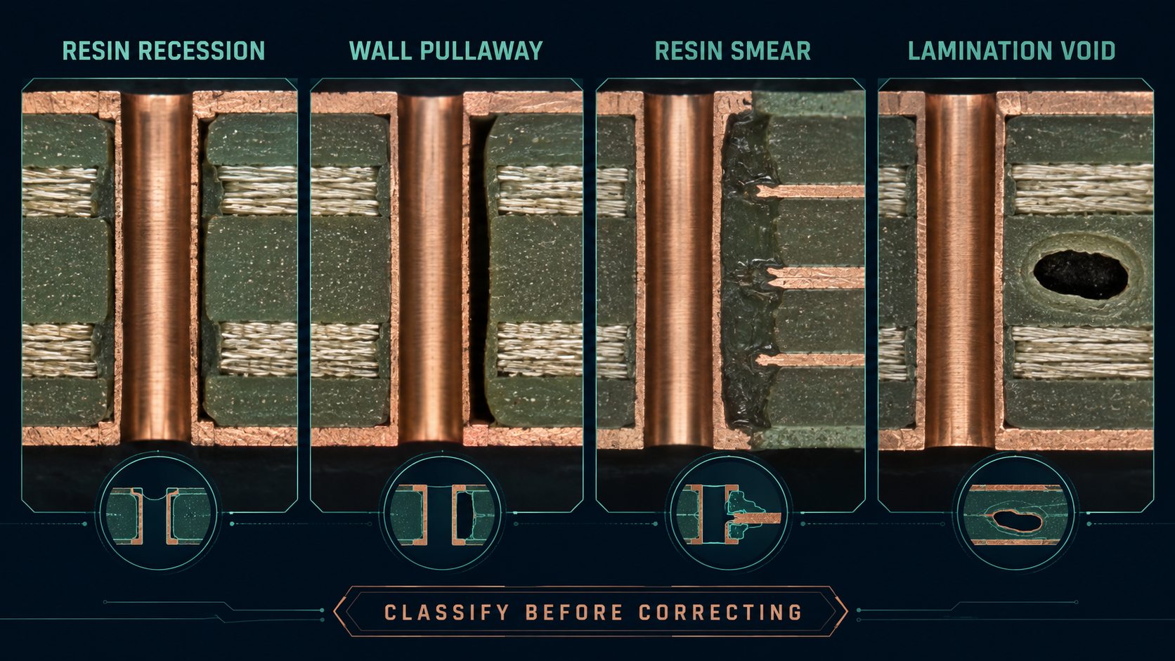
Resin Recession vs Hole Wall Pullaway, Smear, Starvation, and Voids

Classify the material or interface that is missing, displaced or separated before selecting corrective action.

Finding Defining location Key visual clue Investigation focus
Resin recession Resin boundary near glass/copper Resin sits back while reinforcement or adjacent geometry is exposed Material, lamination, thermal history and preparation artifact
Hole wall pullaway Copper-barrel-to-dielectric interface Gap follows the interface beside an otherwise recognizable barrel Interface preparation and interconnect reliability
Resin smear Drilled wall or inner-layer connection Resin coats or obscures copper that should be exposed Drilling heat and desmear effectiveness
Resin starvation Broader laminate region Insufficient resin wet-out around reinforcement Prepreg selection, layup and resin flow
Lamination void Inside the dielectric Enclosed cavity rather than a recessed surface boundary Layup, vacuum, pressure and entrapped volatiles
Comparison of PCB resin recession, hole wall pullaway, resin smear and lamination void morphologies
Similar-looking cross-section findings can point to different process checks; classify before correcting.

For a focused explanation of copper-interface separation, use our PCB hole wall pullaway guide. The distinction matters because increasing desmear, changing a press cycle or altering a plating process are not interchangeable remedies.

Why Recession Can Become More Visible After Thermal Stress

Thermal exposure can change the apparent or actual geometry because resin, glass and copper respond differently to heat, moisture and repeated expansion. This does not mean thermal stress is always the original cause. It may reveal a pre-existing material or process weakness, exaggerate a preparation-related feature, or create a condition beyond the product’s normal use.

Always identify whether the section was examined as received, after baking, after solder float, after reflow simulation, or after another conditioning sequence. Record temperature, dwell, cycles, ramp, cooling and moisture conditioning. Without that information, a before/after comparison cannot be reproduced.

When the concern appeared after assembly, include the actual reflow and rework history. Multiple local rework cycles may produce a different exposure from one qualified production profile. Our solder float test guide explains why the specified test method and post-stress evidence must travel together.

A Microsection Sequence That Preserves Evidence

A controlled sequence should produce comparable sections without consuming every suspect sample.

  1. Identify part, revision, lot, panel position, hole type and downstream history.
  2. Reserve untested specimens and known-good comparison material.
  3. Photograph the board and mark the intended section plane.
  4. Mount and support the specimen so the hole remains centered and edges are protected.
  5. Grind and polish progressively, avoiding excessive heat or pressure.
  6. Capture a full-hole overview before higher-magnification details.
  7. Record resin, glass, barrel and inner-layer geometry separately.
  8. Apply any agreed thermal stress to a separate or documented specimen group.
  9. Compare frequency and extent across locations, lots and conditions.
  10. Retain images, raw measurements, unused samples and the preparation record.

A single attractive micrograph is not a sampling plan. For broader specimen and report requirements, see how PCB microsection analysis finds hidden defects.

Unsure whether the section shows recession or another defect?

Send the original overview and detail micrographs, stackup, material callout, drill data, sample condition and thermal history. EBest Circuit can identify what additional evidence is needed before a process change or rebuild.

Material and Lamination Conditions to Investigate

Resin recession can reflect the material system, its condition and the way the multilayer was laminated, but no one factor should be declared causal without correlation.

Area Question Evidence
Material construction Is the prepreg/resin system appropriate for the stackup and thermal exposure? Controlled stackup, material designation and supplier lot
Storage and handling Could moisture or out-of-control storage affect behavior? Receiving, storage, floor-life and bake records
Layup Is resin distribution consistent around dense copper and drilled regions? Artwork, copper balance, prepreg selection and panel map
Press cycle Did temperature, pressure, vacuum and cure remain within the controlled recipe? Actual press chart and lot traveler
Thermal history Was the construction exposed beyond the qualified sequence? Fabrication, assembly, rework and test profiles

Compare the finding with resin-rich and resin-poor areas, different panel locations and more than one material lot. If the feature follows copper density rather than the drill tool, lamination and local resin-flow evidence deserve closer attention.

Drilling and Hole Preparation Checks

Drilling and desmear determine the surface that later receives metallization, so their records help distinguish true recession from smear, roughness or preparation damage.

  • Review drill diameter, tool type, hit count and actual tool-change interval.
  • Check feeds, spindle speed, entry/backer materials and panel stack height.
  • Inspect unplated hole walls when retained process coupons are available.
  • Compare high-copper and low-copper panel regions.
  • Review desmear chemistry, concentration, temperature, dwell, loading and agitation.
  • Confirm conditioning and metallization followed the controlled process window.
  • Look for smear, glass-fiber protrusion, gouging, voids and barrel discontinuity as separate findings.

Do not respond to suspected recession by simply increasing chemical attack. An aggressive change may alter the hole wall in another way. Trial the cause-specific adjustment and compare controlled sections.

How to Read Extent, Location, and Frequency

The decision value of a finding comes from its distribution, not only its maximum-looking example. Record how many inspected holes show the condition, where it appears around each circumference, its approximate extent and whether it clusters by layer, panel region, hole size or thermal condition.

A repeated feature at the same depth can point toward construction or process interaction. A feature concentrated near one panel edge may justify reviewing press or chemistry uniformity. A correlation with one drill tool suggests a different path. No correlation is also evidence: it means the investigation should remain open rather than forcing the first explanation.

Use measurement methods agreed by the customer, supplier and applicable specification. Avoid extracting a universal acceptance limit from an unrelated image or article; product class and customer requirements control the final disposition.

Containment Before Root Cause Is Confirmed

Containment protects product and evidence while the investigation is still uncertain.

  1. Identify the suspect lot boundaries and all downstream locations.
  2. Segregate suspect, screened, accepted and rebuilt material.
  3. Preserve traceability to panels, materials, drill tools and press/plating batches.
  4. Reserve representative samples before destructive analysis.
  5. Define any temporary screen and document what it cannot detect.
  6. Stop uncontrolled extra thermal exposure that could change the evidence.
  7. Assign disposition authority and a deadline for the next evidence review.

Containment does not prove acceptability. If product has already entered assembly or the field, risk evaluation must include application, thermal/mechanical stress and the possibility of associated interconnect defects.

Cause-Specific Corrective Actions and Verification

A corrective action is credible only when it follows confirmed evidence and passes a controlled verification.

Evidence pattern Action direction Verification
Material or storage-lot correlation Correct material control, conditioning or approved construction Traceable comparison build and repeat sections
Press-cycle or panel-position correlation Restore recipe, vacuum, pressure or loading uniformity Actual press chart plus mapped microsections
Drill-tool correlation Adjust tool-life/parameter control Controlled drill trial before and after plating
Preparation artifact Correct mounting, grinding and polishing method Independent repeat sections
Excess downstream thermal exposure Control assembly/rework profile Qualified profile followed by agreed inspection

Changing material, drilling, desmear and lamination simultaneously can hide the true contributor. When practical, isolate variables and retain the evidence that proves the improved outcome is repeatable.

What to Send for Supplier Engineering Review

A review can move faster when design data, specimen identity and process history arrive together.

  • Gerber or ODB++, fabrication drawing and controlled revision;
  • stackup, material designation and prepreg construction;
  • NC drill files, drill table and relevant hole structures;
  • product class, customer specification and acceptance question;
  • lot, panel and sample traceability;
  • full-resolution overview/detail micrographs;
  • sample preparation method and operator/lab identity;
  • thermal conditioning, soldering and rework profiles;
  • quantity affected, containment status and required response date;
  • target build quantity and delivery requirement if a rebuild is requested.

Prepare a controlled PCB review or rebuild package

Include the design files, material/stackup, drill data, acceptance requirement, original images and thermal history. We will separate the immediate containment question from DFM, inspection and production requirements.

FAQ About PCB Resin Recession

Is resin recession always a rejectable PCB defect?

No universal answer applies. The governing product/customer requirement, morphology, extent, sampling, associated defects and end-use risk determine disposition.

Is resin recession the same as hole wall pullaway?

No. Recession describes resin pulled back from its expected boundary. Pullaway describes separation at the copper-barrel-to-dielectric interface. Both can appear near a plated hole.

How is resin recession different from resin smear?

Smear is unwanted resin left on a drilled wall or inner-layer copper. Recession is resin absent or set back relative to surrounding geometry.

Can polishing create apparent resin recession?

Yes. Differential removal of soft resin, glass and copper can produce relief. Repeat preparation and comparison specimens help test that explanation.

Can visual inspection find resin recession?

Usually not from the PCB surface. A controlled cross-section is normally needed to see and interpret the internal geometry.

Does thermal stress cause every case?

No. Thermal exposure may reveal or enlarge a condition, but material, lamination, drilling, preparation and specimen artifacts must also be investigated.

What should a microsection image include?

Include a full-hole overview and detailed views with scale or magnification, sample identity, orientation, preparation condition and thermal history.

How many holes should be inspected?

The sampling plan should reflect the governing requirement, lot risk and observed distribution. One hole cannot normally establish lot-wide frequency.

Can electrical test prove the laminate interface is acceptable?

No. Electrical continuity can pass while a structural finding remains. Use electrical results with microsection, process and reliability evidence.

What proves a corrective action worked?

A traceable controlled build using the confirmed change, followed by the agreed sampling, conditioning and inspection sequence, provides stronger proof than a single passing section.

Final Acceptance and Prevention Checklist

  • Confirm the feature is real and not specimen-preparation relief.
  • Differentiate recession from pullaway, smear, starvation and voids.
  • Define sample count, distribution and thermal condition.
  • Use the correct customer or product acceptance requirement.
  • Preserve lot, panel, material and process traceability.
  • Link root cause to physical and process evidence.
  • Verify the specific correction on a controlled build.
  • Update drawings, inspection plans and supplier records where needed.

Get an evidence-led PCB manufacturing review.

Send Gerber or ODB++, stackup, drill files, material callout, micrographs, lot history, thermal profile, quantity and target delivery to sales@bestpcbs.com, or use the PCB quote form. EBest Circuit will identify missing evidence and align inspection requirements before production or a corrective rebuild.


You may also like

Solder Float Test PCB: Procedure, Defects and Inspection
Thursday, August 6th, 2026

A solder float test PCB evaluation requires a production-representative coupon, controlled molten-solder exposure, and PTH inspection against an invoked acceptance specification. A record that says only “288°C for 10 seconds, pass” omits moisture conditioning, solder contact, exposure count, hole construction, section location, and the disposition criterion.

The test creates a steep temperature gradient from the solder-contact face into the laminate. Copper and the resin-glass system expand differently, so marginal barrel plating, corner geometry, internal-layer connections, and laminate interfaces can open or separate.

Solder float test PCB coupon above a controlled solder bath in a reliability laboratory

What Is a Solder Float Test for PCB?

A PCB solder float test places a prepared bare-board specimen on molten solder for a specified dwell so that the solder-contact face receives rapid conductive heating. For plated-through-hole thermal stress, the specimen is subsequently microsectioned. The section exposes the copper barrel, knee or corner regions, lands, resin, glass reinforcement, and inner-layer connections that cannot be judged from the exterior surface.

The mechanism is more severe than the temperature number alone suggests. The solder-facing copper heats first while the upper portion of the coupon lags. Through-thickness expansion of the laminate loads the comparatively low-expansion copper barrel in tension. At a plated-hole corner, the load is concentrated where barrel copper changes direction into the surface land. At an inner-layer junction, local resin geometry and copper continuity determine whether the connection remains intact.

IPC-TM-650 Method 2.6.8E is an established method for evaluating the ability of plated-through holes to withstand extreme heat encountered during assembly, rework, or repair. It is a test method, not a universal product acceptance table. The drawing, procurement specification, applicable IPC-6010-series performance specification, or customer requirement must still define the class, sampling, permitted conditions, and disposition criteria.

What Does a Solder Float Test Evaluate?

For structural thermal stress, the test evaluates whether plated-through holes, lands, internal connections, and surrounding laminate remain acceptable after the specified rapid heat exposure. It is most useful for revealing weaknesses that are dormant at room temperature but open when the laminate expands or when moisture becomes vapor.

The evidence can support four narrow decisions. First, did the tested barrel copper remain continuous? Second, did the copper-to-inner-layer connection remain intact? Third, did lands and foil remain attached without prohibited lifting or cracking? Fourth, did the laminate remain free from prohibited blistering, delamination, or other heat damage?

A pass does not establish component solder-joint reliability, field thermal-cycle life, or survival through every lead-free reflow profile. Solder float heating is one-sided and extremely rapid. Convection reflow heats the board from both sides through a time-temperature profile, while environmental cycling repeatedly changes the entire assembly temperature. These different temperature fields create different strain histories.

Required Decision Relevant Evidence Evidence Not Supplied
PTH survival after the invoked solder-float condition Representative coupon, controlled exposure, and conforming microsection Long-term field life
Surface-finish wetting Wetting coverage and dewetting observations from a solderability method Internal barrel integrity
Survival of the intended reflow process Assembly simulation using the intended profile and number of excursions Established by solder float alone
Reliability of assembled solder joints Assembly-level cycling, monitoring, and failure analysis Established by a bare-board coupon

Which Standards Apply to PCB Solder Float Testing?

The correct standard depends on whether the decision concerns PTH thermal integrity, flexible-material resistance, reflow simulation, or termination solderability. Using a solder pot does not make these methods interchangeable.

Document or Method Controlled Scope Engineering Use
IPC-TM-650 2.6.8E Thermal stress of plated-through holes Conditioning, solder-float exposure, and subsequent microsection evaluation
IPC-TM-650 2.6.27 Convection-reflow assembly simulation Closer representation of an intended surface-mount reflow profile
IPC-TM-650 2.4.13F Solder-float resistance of flexible printed wiring materials Material evaluation within the method’s stated flexible-circuit scope
J-STD-003 Solderability of printed boards Wetting acceptance for designated board terminations
Applicable performance or customer specification Product acceptance Class, sample quantity, allowed defects, and lot disposition

A test plan should state the document number, revision, condition, number of exposures, and acceptance document. Writing only “IPC solder float” leaves the laboratory to choose among different purposes and conditions. That ambiguity becomes especially serious when a supplier interprets the request as a wetting test while the customer expects a microsectioned PTH thermal-stress result.

Increasing the number of solder-float exposures does not reproduce a convection-reflow profile. Qualification must match the product’s heat-transfer mode, temperature history, and expected failure mechanism.

How Should PCB Samples Be Prepared Before a Solder Float Test?

Sample preparation must control moisture, confirm coupon representation, and document a defect-free baseline before the specimen touches solder. Otherwise, the laboratory cannot distinguish a manufacturing defect from conditioning damage or test handling.

For the referee procedure in IPC-TM-650 2.6.8E, specimens are dried for a minimum of six hours at 121–149°C and cooled in a desiccator. That conditioning removes uncontrolled moisture as a test variable. It should not be silently substituted when the purchase requirement calls for an as-received or moisture-preconditioned evaluation, because drying can suppress moisture-driven delamination that the customer intended to assess.

Match the coupon to the production board’s thickness, layer count, material designation, surface finish, finished and drilled hole diameters, copper weights, plating process, and inner-layer connection pattern. Record the material lot when available. High aspect-ratio holes, small finished diameters, heavy copper distribution, and resin-starved local constructions may experience more strain than an easier coupon.

Inspect and photograph the specimen before exposure. Reject or separately document pre-existing blisters, land damage, plugged holes, contamination, edge damage, or suspected delamination. If continuity monitoring is required, record the baseline resistance and measurement path. The laboratory should also identify which holes will be sectioned so that convenient, visually clean holes are not selected only after the test.

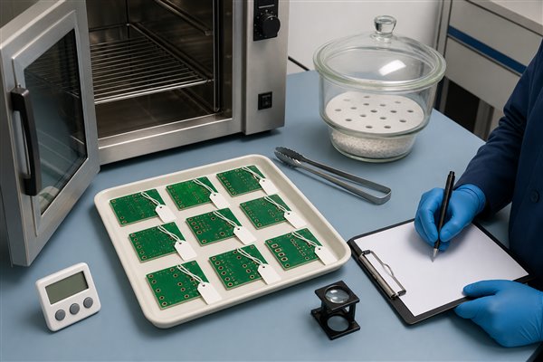
PCB sample preparation and traceability before a solder float test

Apply the flux required by the method to the plated holes and relevant specimen surface. Flux quantity and coverage affect wetting and therefore the consistency of thermal contact. Excess residue can also conceal surface evidence. The preparation record should state the flux identification, lot or expiration control where required, application method, and any permitted preheat.

How Is a Solder Float Test for PCB Performed?

The procedure verifies bath condition, places the prepared specimen on a clean solder surface for the timed dwell, removes it without shock, cools it as specified, and transfers it to controlled inspection. Each step affects the actual thermal load.

  1. Stabilize and verify the bath. Confirm the required solder composition and temperature at the specified measurement location. A controller display does not prove that the contact surface is within tolerance.
  2. Prepare a clean contact surface. Remove dross as permitted by the procedure. Oxide or dross can hold part of the coupon above the liquid solder and create uneven heating.
  3. Flux the specified areas. Use the required flux and application method. Do not add an unapproved preheat or extended activation time.
  4. Start consistent contact. Lower the specimen flat onto the molten solder without forcing it below the surface. The timing reference must be consistent from specimen to specimen.
  5. Control the dwell. IPC-TM-650 2.6.8E specifies a ten-second exposure with a +1/-0 second tolerance for its listed conditions. The invoked requirement controls the actual test.
  6. Remove without mechanical damage. Do not bend, shake, scrape, or shock the specimen while the solder remains liquid. Mechanical loading at that moment can create damage that is not attributable to thermal stress alone.
  7. Cool and repeat only as specified. Record cooling time and method between exposures. An unrecorded hot restart changes the starting temperature and accumulated strain.
  8. Clean, inspect, and section. Preserve visible evidence before destructive preparation. Maintain traceability between the specimen, photographed surface, selected holes, and finished microsection.

The operator should record the actual bath temperature and dwell for each exposure, not only the nominal recipe. If a specimen rocks, traps gas, loses full contact, or is accidentally pushed into the bath, mark the run invalid and repeat with a new qualified specimen rather than averaging the event into a pass.

Which Parameters Control Solder Float Test Severity?

Severity is determined by the combined temperature, dwell, starting condition, contact quality, exposure count, cooling history, specimen geometry, and material response. Two laboratories can use the same nominal bath temperature and produce different stress when these other variables are uncontrolled.

Parameter Effect on the Specimen Control or Record
Bath temperature Changes heat flux and peak temperature reached during the dwell Actual value, tolerance, probe location, and verification time
Dwell time Changes heat penetration and copper-laminate strain Actual time for every exposure and timing reference
Starting temperature and moisture Changes thermal gradient and vapor-pressure contribution Drying, storage, desiccator cooling, and preconditioning history
Solder contact Controls whether heating is uniform across the face Dross removal, flat placement, flux coverage, and anomaly notes
Exposure count and cooling Changes accumulated damage and recovery between events Number of passes, interval, cooling method, and restart temperature
Coupon construction Changes strain concentration and heat flow Thickness, layer count, hole geometry, plating, copper distribution, and material

Method 2.6.8E lists Condition A at 288±5°C, Condition B at 260±5°C, and Condition C at 232±5°C. These are method conditions, not a menu from which the laboratory should pick the most convenient value. The procurement document must invoke the condition or provide the governing product requirement.

A higher temperature cannot compensate for poor process definition. A short exposure at 288°C and a longer exposure at 260°C do not necessarily create equivalent strain because the heating rate, peak temperature distribution, resin response, and interfacial stress differ. Equivalence requires validated correlation for the construction, not a simple temperature-time trade.

What PCB Defects Can a Solder Float Test Reveal?

The test can reveal thermally activated cracks and separations in the PTH structure, lands, internal connections, and laminate. The defect name alone is insufficient; location, orientation, extent, and connection to the functional conductor determine the risk.

  • Barrel cracking: a circumferential or partial crack through the plated copper wall. It may open under expansion and close again after cooling, so a room-temperature continuity check can miss it.
  • Corner or knee cracking: a crack at the transition from barrel copper to the surface land. The geometric change concentrates strain, particularly when copper thickness or local plating geometry is marginal.
  • Inner-layer connection separation: loss of intimate connection between the plated barrel and an internal copper feature. Sectioning must pass through the relevant connection; a nearby plane can miss the discontinuity.
  • Land lifting or land separation: upward movement or separation of a surface land from the laminate. Distinguish true thermally induced lifting from damage introduced during section preparation.
  • Foil cracking: cracking in surface or internal copper adjacent to the hole. Record whether the crack reaches a functional conductor.
  • Blistering: a localized raised area caused by separation or volatile pressure beneath a surface layer. Photograph it before grinding destroys the external evidence.
  • Delamination: separation between laminate plies or at another interface. Report its location, length, relationship to conductors, and whether it was present before exposure.
  • Resin recession or resin damage: changes around the hole wall that must be judged using the invoked specification and preparation quality rather than an improvised limit.

Failure morphology guides the investigation but does not prove a single root cause. Barrel or corner cracks may direct attention to plating thickness, copper ductility, hole preparation, geometry, and laminate expansion. Delamination may require review of moisture history, lamination bonding, resin distribution, material compatibility, and the validity of the exposure. A corrective action should not be assigned until the defect is confirmed in representative sections and correlated with manufacturing records.

How Should PCB Solder Float Test Results Be Inspected?

Inspect the specimen in a fixed sequence so each internal finding remains traceable to its pre-test condition and coupon location. Cleaning, cutting, or etching out of sequence can destroy evidence needed for disposition.

  1. Preserve the surface condition. Photograph the specimen before cleaning or cutting. Record blistering, land movement, discoloration, surface damage, solder obstruction, and handling anomalies.
  2. Repeat required electrical checks. Compare continuity or resistance with the baseline. Stable room-temperature continuity does not exclude a crack that opened only while hot.
  3. Select holes without bias. Use locations defined by the test plan or a documented random method. Inspecting only the cleanest or worst-looking hole can distort the lot decision.
  4. Cut near the hole centerline. An off-center section can exaggerate plating thickness, omit an inner-layer connection, or hide a partial barrel crack.
  5. Examine the as-polished section. Check barrel and corner cracks, land separation, voids, laminate separation, and plating continuity before etching changes the contrast.
PCB microsection inspection of plated through holes after solder float testing
  1. Microetch only when required. Use the etched condition to clarify copper interfaces and boundary detail; retain both views because etched and as-polished images are not interchangeable.
  2. Confirm isolated findings. Prepare another plane or serially grind when a suspected defect appears in only one section. Do not assign a lot-wide root cause from one ambiguous feature.
  3. Separate artifacts from defects. Check whether edge rounding, pullout, scratches, smearing, or overetching created the observed feature.
  4. Document the disposition. Record the coupon and hole location, magnification, scale, defect orientation, image condition, and exact acceptance clause.

How Does the Solder Float Thermal Stress Test Differ from a Solderability Test?

Structural solder-float testing asks whether the PCB construction survives rapid heating; solderability testing asks whether specified metallic terminations wet with solder. Both can use molten solder, but they inspect different objects and produce different acceptance evidence.

Decision Element Structural Solder Float Solderability Test
Primary question Did the PTH and laminate remain structurally acceptable? Did the designated surface wet as required?
Primary observation Microsectioned barrel, lands, interfaces, and laminate Wetting coverage, nonwetting, and dewetting
Typical concern Cracking, separation, blistering, or delamination Oxidation, finish condition, contamination, or poor wetting
Applicable method family Thermal-stress and product-performance requirements J-STD-003 or another invoked solderability procedure

A board can wet well and still contain a thermally damaged barrel. It can also retain sound internal structure while an aged or contaminated surface finish wets poorly. If both risks matter, specify both tests and keep their sample preparation and acceptance records separate. A PCB solderability test should not be reported as PTH thermal-stress evidence.

How Does Solder Float Testing Differ from Thermal Cycling and Thermal Shock?

Select the method by heat-transfer mode, repetition, monitored object, and required reliability decision. Solder float is not a faster substitute for a chamber-based qualification.

Comparison Solder Float Thermal Cycling Thermal Shock
Heat input Rapid conductive heating from the solder-contact face Controlled chamber heating and cooling of the whole specimen Rapid transfer between hot and cold environments
Exposure pattern One or more short method-defined dwells Repeated ramps, dwells, and cycles Repeated abrupt temperature transitions
Primary stress Steep through-thickness gradient and PTH strain Cyclic expansion and fatigue accumulation High strain rate from rapid environmental change
Typical test object Bare-board coupon or representative PCB specimen Bare board or assembled product with monitoring Board, assembly, material, or component as specified
Best use PTH and laminate response to rapid assembly-like heat Fatigue and intermittent opens over repeated temperature excursions Resistance to abrupt temperature change
Key limitation Does not reproduce a chamber profile or field cycling Does not reproduce direct molten-solder contact May be more abrupt than the intended operating environment

Use convection-reflow simulation when the intended assembly profile must be represented. Use a broader PCB thermal stress test plan when repeated environmental transitions, solder-joint fatigue, or monitored field reliability is the required decision.

What Should a PCB Solder Float Test Report Include?

A defensible report must allow another qualified laboratory to identify the same specimen, reproduce the exposure, inspect equivalent locations, and apply the same acceptance rule. A pass/fail certificate without this chain is weak procurement evidence.

  • Requirement: test method, revision, condition, applicable performance specification, class, customer deviations, sample quantity, and acceptance clause.
  • Specimen identity: part number and revision, panel or coupon identity, lot, material and construction, board thickness, layer count, hole type and size, and relevant plating information.
  • Conditioning: drying or moisture preconditioning, temperature and duration, storage after conditioning, desiccator use, and elapsed time before testing.
  • Bath controls: solder alloy, flux, bath setpoint and actual verification, measurement location, surface preparation, and equipment identification or calibration status as required.
  • Exposure record: actual dwell, number of passes, cooling interval and method, specimen orientation, contact anomalies, and operator observations.
  • Inspection evidence: pre- and post-test photographs, electrical results when required, section map, evaluated hole locations, as-polished and etched images, scale, magnification, and defect annotations.
  • Disposition: result for each specimen, exact acceptance clause, nonconformance description, reviewer, and authorization of the final report.

Procurement teams should reject ambiguous substitutions. If the purchase order invokes Condition A and microsection evaluation, a supplier should not close the requirement with a wetting photo, an unsectioned coupon, or a certificate that omits the actual condition. Any deviation should be approved before testing, not explained after a failed lot.

What Can Make Solder Float Test Results Misleading?

Results become misleading when coupon representation, moisture history, real bath contact, timing, cooling, or section selection differs from the stated test. These controls can produce false confidence or false rejection even when the nominal temperature is correct.

  • Unrepresentative coupons: easier holes or a different material construction can hide the production board’s highest-strain feature. Compare coupon design and panel location with the actual stackup.
  • Uncontrolled moisture: unknown storage may add vapor-pressure damage, while unapproved drying may remove the moisture sensitivity the requirement intended to test.
  • Temperature measured at the wrong location: the controller or a distant probe can be within tolerance while the specimen-contact region is not.
  • Dross or incomplete contact: part of the coupon may float above the liquid surface, reducing local heat input and producing a false pass.
  • Forced immersion or rocking: changing immersion depth or mechanically loading the coupon introduces a different exposure and possible handling damage.
  • Timing drift: starting the timer before full contact or stopping it after removal changes the real dwell. Record a consistent event definition.
  • Uncontrolled cooling: repeating while the specimen is still hot increases accumulated stress; excessive forced cooling can introduce a different thermal shock.
  • Mechanical shock while solder is liquid: bending or impact can create copper or land damage that the thermal method alone did not cause.
  • Convenience sectioning: inspecting only easy or visually clean holes can miss a localized failure. Predefine or randomly select the evaluated locations.
  • Preparation artifacts: off-center grinding, pullout, overetching, and poor edge retention can mimic or conceal defects. Confirm uncertain features in another preparation plane.

When a specimen fails, preserve the original coupon, photographs, bath records, and remaining unsectioned holes. Confirm the feature in additional locations, compare it with an unexposed baseline, and review the relevant manufacturing records. Only then separate a material or fabrication issue from an invalid test event or a nonrepresentative coupon.

FAQs About Solder Float Test PCB

Q1: What temperature should be specified for a PCB solder float test?

Use the temperature and tolerance invoked by the selected test method and product requirement. IPC-TM-650 2.6.8E lists Conditions A, B, and C at 288±5°C, 260±5°C, and 232±5°C respectively. The drawing or procurement document should identify the condition rather than leaving the laboratory to choose.

Q2: How hot is too hot for a PCB during solder float testing?

The exposure is too hot when the actual bath exceeds the invoked tolerance or when an unapproved condition is used for that construction. There is no universal PCB damage temperature because material system, thickness, moisture, hole geometry, dwell, and prior thermal history all affect the response.

Q3: What is a PCB test coupon?

It is a traceable test vehicle designed to represent specified production-board features. For solder-float PTH evaluation, it should contain the relevant hole sizes, plating, layer connections, material, and thickness. A coupon is not representative merely because it came from the same panel.

Q4: Should PCB testing be completed before soldering components?

Bare-board acceptance testing should be completed before assembly when required by the procurement plan. This prevents component value and assembly work from being added to a nonconforming board lot. Assembly-process simulation may still require separate samples and the intended reflow profile.

Q5: What problems can PCB delamination cause?

Delamination can reduce mechanical support, disturb conductor geometry, propagate toward plated holes, trap contaminants, or develop into an electrical reliability risk. Disposition depends on its interface, size, location, relationship to conductors, and the applicable acceptance specification.

Q6: Does the solder alloy’s melting temperature define the test temperature?

No. The invoked test condition defines the controlled bath temperature. The alloy must be appropriate for the method, but its melting range does not replace the specified temperature, tolerance, dwell, or acceptance requirement.

Q7: How should a PCB be inspected after a solder float test?

Preserve surface evidence first, complete required electrical checks, and then examine traceable microsections in the required as-polished and etched conditions. Record the evaluated holes, section plane, magnification, scale, defect location, and acceptance clause.

Q8: What standard controls PCB inspection after thermal stress?

The test method controls preparation and exposure, while the applicable product or customer specification normally controls acceptance. The report should cite both documents and their revisions so that the pass/fail basis is auditable.

Q9: Can solder float testing replace other PCB test methods?

No. It answers only the structural or solderability decision explicitly defined by the invoked procedure. Electrical test, reflow simulation, ionic cleanliness, insulation resistance, environmental cycling, and assembly-level reliability tests address different risks.

Q10: Is a solder float test suitable for every PCB construction?

Not automatically. Flexible materials, rigid boards, unusual laminates, thick constructions, microvias, and products with process-specific qualification needs may require different or additional methods. Select the test from the construction, assembly profile, failure mechanism, and governing specification.

Conclusion

A defensible result must connect representative hardware, controlled exposure, traceable inspection, and an applicable acceptance rule. A solder float test PCB evaluation cannot be reduced to temperature and dwell. Coupon geometry, moisture history, contact quality, cooling, section location, and defect interpretation determine whether the result can support a manufacturing or procurement decision.

For a PCB quotation or test-plan review, email sales@bestpcbs.com with the Gerber or ODB++ data, stackup, material requirement, board thickness, layer count, finished-hole range, copper requirements, surface finish, quantity, applicable specification, assembly profile, and required inspection or test documentation.

You may also like