

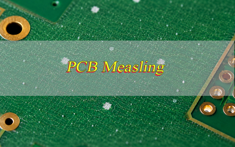
PCB measling is a laminate defect that appears as small white marks inside the PCB base material. It is usually caused by local resin-to-glass separation after thermal stress, moisture exposure, drilling stress, lamination variation, or assembly heating.
In many cases, small and isolated measling is not an immediate functional failure. However, it should never be ignored. It may show that the PCB material, storage condition, soldering profile, or fabrication process is not fully controlled. For reliable PCB manufacturing and PCBA assembly, measling should be inspected, classified, and prevented before it affects production quality.
What Is PCB Measling?
PCB measling is a subsurface laminate condition where small white marks appear inside the PCB base material, usually near glass fiber intersections. These marks are caused by local separation between epoxy resin and woven glass reinforcement.
Measling in PCB is different from board cracking, burning, or complete layer separation. It is normally small, scattered, and visible through the laminate or solder mask. The board surface often remains flat in mild cases.
The key point is that PCB measling is a stress signal. Even if the circuit passes electrical testing, the defect should still be reviewed because it may indicate moisture absorption, weak laminate bonding, or excessive thermal stress during fabrication or assembly.
What Does Measling in PCB Look Like?
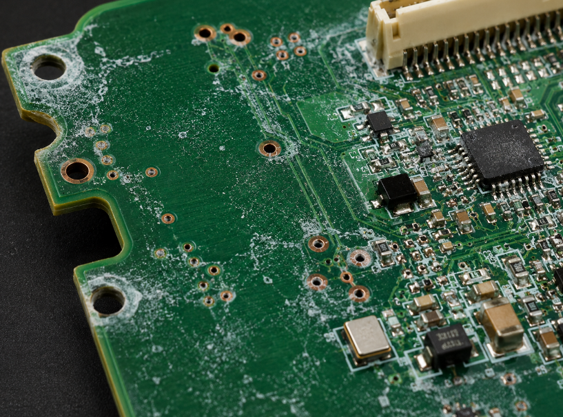
PCB measling defect appearance usually includes small white, dot-like, square-like, or cloudy marks under the laminate surface. These marks look trapped inside the board instead of sitting on the solder mask or copper surface.
Common visual signs include:
- Small white dots inside FR-4 laminate
- White square marks near woven glass fiber crossing points
- Local cloudy areas under the solder mask
- Flat surface without swelling or bubbles
- No obvious copper lifting in mild cases
- No long continuous crack line across the board
Inspection should not judge the defect only by color. The location, size, density, nearby copper features, surface condition, and change after thermal exposure should all be checked before deciding whether the board is acceptable.
Why Does PCB Measling Matter for Board Reliability?
PCB measling matters because it shows that the laminate has experienced stress outside the ideal process window. A single isolated white mark may not stop the board from working, but repeated marks across a batch may suggest a larger process problem.
The real concern is not only the white appearance. The concern is whether the board also has moisture absorption, poor resin cure, weak lamination, excessive reflow stress, unsuitable material, or hidden delamination risk.
For high-reliability products, measling can affect confidence in long-term performance. This is especially important for industrial control, automotive electronics, telecom equipment, medical devices, power modules, and high-voltage PCB assemblies where insulation strength and stable laminate structure matter.
What Causes PCB Measling?
The main causes of PCB measling include trapped moisture, thermal shock, weak resin-to-glass bonding, drilling stress, improper lamination, and aggressive soldering profiles. These factors create local stress inside the laminate.
Common causes include:
- Moisture absorption: absorbed moisture expands quickly during reflow, wave soldering, selective soldering, or rework.
- High thermal shock: fast heating makes resin and glass expand at different rates.
- Improper lamination: poor resin flow, cure control, or pressure control weakens laminate bonding.
- Rough drilling or routing: mechanical stress can create local whitening near holes, slots, and edges.
- Unsuitable material: low Tg or weak thermal stability increases risk during high-temperature assembly.
- Repeated rework: multiple heating cycles can turn a small visual issue into a reliability concern.
What causes PCB measling is usually not one single problem. It is often the combined result of material selection, storage control, fabrication process, and assembly heat exposure.
Where Does Measling PCB Defect Commonly Appear?
Measling PCB defect commonly appears where laminate stress, moisture, drilling force, or soldering heat is concentrated. The location matters because the same visual mark may have different reliability risks in different areas of the board.
Common appearance areas include:
- Around drilled holes: drilling pressure, worn drill bits, poor debris removal, or local barrel stress may create white marks near plated through holes and vias.
- Near routed edges and slots: routing pressure exposes laminate edges and may trigger local whitening if the board material is brittle or poorly supported.
- Under solder mask: some marks remain hidden until inspection under proper lighting, especially on dark solder mask colors.
- Near high-copper areas: heavy copper, large copper planes, or uneven copper distribution can create uneven thermal expansion during soldering.
- Around BGA and fine-pitch areas: concentrated reflow heat and local board stress can make hidden laminate weakness visible after assembly.
- Near connectors and terminals: insertion force, soldering heat, and local mechanical load may increase stress around connector pads.
- Large open laminate areas: weak resin flow, uneven cure, or material handling issues may show as scattered white marks across the panel.
- Thick multilayer PCB areas: thicker boards hold more internal stress and may react more strongly to thermal shock or moisture expansion.
Measling far from conductors may be less critical, but marks near plated holes, high-voltage spacing, edge plating, dense components, or controlled-impedance areas need stricter review. The defect should be judged by location, density, process history, and final product risk.
What Is the Difference Between Measling and Delamination?
The difference between measling and delamination is that measling is localized resin-glass separation, while delamination is separation between laminate layers or between copper and laminate. Delamination is normally more serious because it can damage structural integrity and electrical insulation.
| Item | Measling | Delamination |
|---|---|---|
| Basic meaning | Local resin-glass separation | Layer-to-layer or copper-to-laminate separation |
| Appearance | Small white dots, squares, or cloudy marks | Bubbles, lifted areas, cracks, layer gaps, or swelling |
| Surface condition | Usually flat in mild cases | Often raised, blistered, or visibly separated |
| Common location | Around glass weave intersections | Between prepreg/core layers, copper interface, or plated areas |
| Main trigger | Local thermal, moisture, or mechanical stress | Severe heat, moisture, poor lamination, or adhesion failure |
| Electrical risk | Usually low when isolated and away from circuits | Higher risk of opens, shorts, leakage, or dielectric failure |
| Structural risk | Limited in mild isolated cases | Can weaken board structure and copper adhesion |
| Inspection method | Visual inspection, magnification, thermal review | Visual inspection, cross-section, thermal stress testing |
| Acceptance focus | Size, density, location, and product class | Separation area, depth, electrical impact, reliability risk |
| Typical action | Record, inspect, monitor, and review process | Investigate root cause and reject when reliability is affected |
PCB measling vs delamination is a common inspection issue because both defects can look white or cloudy. The practical judgment is whether the defect is local and flat, or whether it shows real layer opening, swelling, copper lifting, spreading, or failed electrical testing.
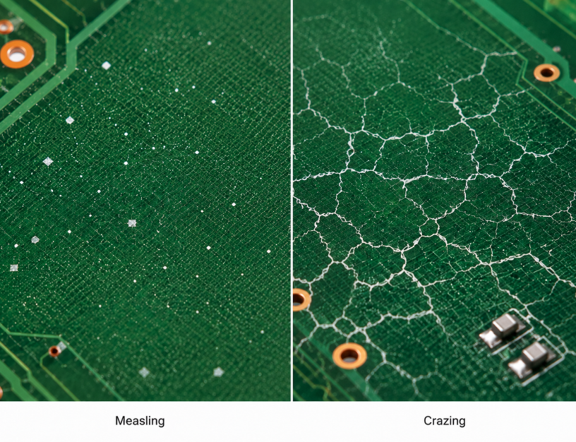
What Is the Difference Between Measling and Crazing?
The difference between measling and crazing is mainly the visual pattern and stress direction. Measling appears as isolated white spots, while crazing appears as connected white lines or streaks along glass fiber bundles.
| Item | Measling | Crazing |
|---|---|---|
| Visual pattern | Dot-like, square-like, or cloudy marks | Line-like, streak-like, or network marks |
| Shape | Isolated local spots | Connected lines following glass weave direction |
| Stress range | Localized stress point | Wider stress path along fiber bundles |
| Common cause | Local resin-glass separation | Resin fracture or separation along glass fibers |
| Appearance area | Often near glass intersections or stressed zones | Often follows warp and fill direction of glass cloth |
| Surface condition | Usually flat in mild cases | Usually flat unless linked with deeper damage |
| Risk level | Depends on size, density, and location | Depends on length, spread, and proximity to conductors |
| Inspection focus | Count, size, location, nearby circuitry | Line length, direction, spread, and circuit clearance |
| Process meaning | Local material or heat stress | Broader laminate stress or mechanical strain |
| Review action | Inspect and compare with acceptance criteria | Inspect carefully if lines extend near critical features |
Both measling and crazing are related to stress between resin and glass reinforcement. However, crazing can suggest that stress has spread along the glass weave instead of staying as isolated points. For Class 3, medical, automotive, aerospace, power, or high-voltage products, visual inspection should be supported by clear acceptance criteria and additional testing when needed.
How Is PCB Measling Different From Blistering and White Spots?
PCB measling is an internal white laminate mark, blistering is raised separation, and white spots may come from several different sources. The surface condition is the first clue.
Blistering usually appears as a bubble-like or raised area. It may show laminate lifting, solder mask separation, coating separation, or copper adhesion risk. PCB measling usually remains flat because the separation is small and internal.
White spots are a broader visual category. They may come from flux residue, cleaning residue, abrasion, solder mask defects, moisture stains, chemical marks, or laminate stress. Therefore, not every white mark should be called measling. Correct judgment requires visual inspection, magnification, surface review, process history, and sometimes cross-section analysis.
How to Test for PCB Measling During Assembly?
Testing for PCB measling during assembly should follow a clear process: visual inspection, defect recording, process review, electrical testing, and deeper analysis when risk is high. The goal is to confirm whether the issue is only visual or related to structural reliability.
Step 1: Inspect the board visually.
Check the PCB under proper lighting and magnification. Focus on white marks under the laminate surface, not residue on the solder mask. Record whether the marks are dot-like, square-like, cloudy, line-like, or spreading across the board.
Step 2: Mark the defect location.
Record whether the marks appear near plated through holes, vias, routed edges, BGA areas, connectors, high-voltage spacing, edge plating, heavy copper areas, or large laminate fields. Location helps decide whether the defect is low risk or needs deeper review.
Step 3: Compare before and after assembly.
If possible, compare bare board inspection photos with post-reflow or post-wave soldering photos. If the marks appear only after heating, the problem may be linked to moisture absorption, thermal shock, or soldering profile control.
Step 4: Review storage and baking records.
Check whether the PCB was vacuum sealed, stored in a dry environment, exposed to humidity, or baked before assembly. Moisture history is important because absorbed moisture can expand rapidly during soldering and create visible laminate stress.
Step 5: Review the soldering profile.
Check reflow peak temperature, ramp rate, time above liquidus, wave soldering temperature, selective soldering dwell time, and hand soldering exposure. Excessive heat or repeated heating can make mild laminate weakness worse.
Step 6: Run electrical tests.
Use continuity testing, flying probe testing, fixture testing, insulation resistance testing, dielectric testing, or functional testing according to the product risk level. A board may look visually questionable but still pass basic electrical testing.
Step 7: Use cross-section analysis when needed.
For high-reliability, high-voltage, automotive, medical, or power products, microsection analysis can confirm whether the issue is only measling or whether hidden delamination, barrel cracks, voids, or deeper resin separation exists.
Step 8: Decide acceptance based on risk.
The final decision should consider defect size, density, location, product class, electrical test result, customer drawing, and IPC acceptance requirements. A mild isolated condition may be accepted, while spreading or critical-location defects should be investigated.

Can PCB Measling Be Accepted or Rejected?
PCB measling may be accepted when it is isolated, flat, away from critical conductors, and allowed by the agreed inspection standard. It may be rejected when it spreads, appears near critical areas, or is linked to electrical or structural failure.
Acceptance depends on:
- Product class: Class 3 and safety-critical boards need stricter review.
- Customer drawing: project-specific requirements override general assumptions.
- Defect location: measling near vias, high-voltage spacing, or edge plating carries more risk.
- Defect density: repeated marks across panels suggest unstable processing.
- Test result: failed insulation, continuity, or function testing changes the decision.
- Thermal history: defects after rework or solder shock require process review.
The practical rule is simple. Do not reject every mild isolated case blindly, but do not ignore repeated or growing signs. The final decision should match the product risk level, IPC requirements, and customer acceptance criteria.
How Can PCB Measling Be Prevented in PCB Manufacturing and Assembly?
PCB measling can be prevented by controlling material selection, laminate storage, drilling quality, soldering heat, moisture exposure, and rework cycles. Prevention should start before fabrication, not after white marks appear during assembly.
Effective prevention methods include:
- Select the right laminate: use High-Tg FR-4 or suitable specialty materials for products exposed to high soldering temperature, repeated reflow, or harsh working environments.
- Confirm material traceability: check laminate brand, Tg, CTI, copper weight, board thickness, and storage condition before batch production.
- Control moisture exposure: keep PCB boards sealed, dry, and protected from long air exposure before assembly.
- Bake boards when required: use controlled baking when boards have been stored too long, exposed to humidity, or shipped through high-moisture conditions.
- Optimize lamination parameters: control resin flow, pressure, temperature, and cure time to improve resin-glass bonding stability.
- Improve drilling and routing: use suitable drill bits, stable feed speed, clean routing paths, and proper panel support to reduce mechanical stress.
- Balance copper and stackup: avoid severe copper imbalance because uneven thermal expansion can increase internal laminate stress.
- Control reflow profile: avoid excessive ramp rate, peak temperature, and time above liquidus. The profile should match laminate capability and component requirements.
- Limit repeated rework: repeated hand soldering, hot air repair, or BGA rework can increase local heat stress and moisture expansion.
- Inspect after thermal processes: add post-reflow or post-wave soldering inspection when the product has strict reliability requirements.
- Define acceptance criteria early: confirm IPC class, visual acceptance rules, special product requirements, and reporting format before production.
- Connect fabrication with PCBA feedback: if measling appears during assembly, feedback should return to material storage, lamination, drilling, and soldering process review.
Prevention works best when PCB fabrication and PCBA assembly are managed together. Material review, stackup planning, soldering profile control, incoming inspection, and post-assembly testing should be aligned before mass production begins.
FAQs About PCB Measling
Q1: Does PCB thickness affect the risk of measling?
A1: Yes. Thicker PCB boards can hold more internal stress and moisture than thinner boards. During soldering, heat may not spread evenly through the laminate, especially in multilayer PCB structures. This does not mean every thick board will show measling, but thick boards need better drying, stackup balance, and controlled heating.
Q2: Can long storage time make measling more likely?
A2: Yes. Long storage can increase moisture absorption if packaging is damaged or storage humidity is not controlled. A PCB that looks normal before assembly may show white laminate marks after reflow. For stored boards, check vacuum sealing, desiccant condition, humidity exposure, and baking requirements before production.
Q3: Should PCB boards be baked before assembly?
A3: Baking is useful when moisture exposure is suspected, but it should not be used blindly. Controlled baking can reduce moisture-related stress before soldering. However, wrong baking temperature or excessive baking time may affect solderability, surface finish, or material condition. Baking rules should match laminate type and project requirements.
Q4: Can solder mask hide PCB measling?
A4: Yes. Dark solder mask colors may make internal white marks harder to see. Green, black, or matte solder mask can reduce visibility under normal light. For products with strict appearance or reliability requirements, inspection should use proper magnification, angled lighting, and bare board review before assembly.
Q5: Is functional testing enough to approve a board with measling?
A5: Not always. Functional testing only proves that the board works under the test condition. It may not reveal future insulation weakness, laminate stress, or hidden structural risk. For high-voltage, automotive, medical, telecom, or power PCB assemblies, visual review and reliability testing may also be required.
Q6: Can PCB measling lead to CAF risk?
A6: Measling itself is not the same as conductive anodic filament growth, but poor laminate integrity, moisture, and insulation stress can increase long-term reliability concern. If the marks appear near high-voltage spacing or dense vias, insulation resistance testing and material review should be considered.
Q7: What information should be included in a measling inspection report?
A7: A useful report should include clear photos, board side, defect location, quantity, size range, process stage, soldering history, and test result. It should also identify whether the issue appeared before assembly, after reflow, after wave soldering, or after rework. Clear reporting speeds up root cause analysis.
Q8: Can hand soldering increase measling risk?
A8: Yes. Hand soldering can create concentrated local heat if dwell time is too long or the soldering iron temperature is too high. Connector pins, large pads, and repair areas are common risk points. Controlled temperature, limited dwell time, and reduced repair cycles help lower laminate stress.
Q9: Does copper thickness affect measling behavior?
A9: Heavy copper does not directly create measling, but uneven copper distribution can create uneven heating and expansion. High-copper areas may cool and heat differently from open laminate areas. A balanced stackup and controlled thermal profile help reduce stress during PCB manufacturing and assembly.
Q10: Can PCB measling appear after conformal coating?
A10: It may become harder to inspect after coating because the surface layer changes light reflection. If white marks are suspected, inspection should be completed before conformal coating. Coating should not be used to hide laminate defects. The board condition should be confirmed before protective coating is applied.
Q11: When is microsection analysis necessary?
A11: Microsection analysis is useful when the defect is near plated holes, high-voltage spacing, BGAs, edge plating, or safety-critical circuits. It helps confirm whether the issue is only visual measling or deeper delamination, barrel cracking, voiding, or resin separation. It is especially valuable for batch disputes.
Q12: Can PCB measling affect impedance-controlled boards?
A12: Mild isolated measling away from controlled traces may not change impedance. However, marks near critical dielectric areas, high-speed traces, or reference planes should be reviewed carefully. For RF, telecom, and high-speed digital PCB projects, stable dielectric structure and material consistency are important.
Q13: Should measling limits be written into purchase documents?
A13: Yes. Purchase documents should define IPC class, visual acceptance rules, inspection method, reporting format, and special reliability requirements. This helps avoid unclear judgment after shipment. It also helps the PCB supplier choose suitable material, process controls, inspection steps, and packaging methods before production.
Q14: Can EBest Circuit support PCB measling prevention and analysis?
A14: Yes. EBest Circuit can support material review, stackup review, PCB fabrication, PCBA assembly, inspection, soldering profile review, and defect analysis. For custom PCB and PCBA projects, we can help reduce measling risk through controlled materials, process planning, quality inspection, and batch production feedback.
Conclusion
PCB measling is a local laminate stress sign, not always a direct functional failure. The correct approach is to identify the defect appearance, compare it with delamination and crazing, review moisture and thermal history, test the board according to product risk, and prevent recurrence through material and process control.
For new PCB and PCBA projects, define material requirements, inspection criteria, soldering limits, and acceptance standards before mass production. If you need custom PCB manufacturing, PCB assembly, defect analysis, or batch production support, contact EBest Circuit for a quotation at sales@bestpcbs.com.
You may also like


Tags: causes measling pcb, measling in pcb, measling pcb, pcb measling vs delamination