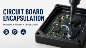
PCB encapsulation is a protective process that covers electronic circuits with resin, gel, or compound to improve durability in demanding environments. It is commonly used when a circuit board needs stronger protection than a thin surface coating can provide.
In many electronic products, a PCB may face moisture, salt spray, dust, vibration, thermal cycling, chemical exposure, or mechanical shock. These conditions can affect long-term reliability, especially in automotive electronics, industrial control systems, LED lighting, power modules, outdoor devices, marine electronics, and high-voltage assemblies.
This guide explains what PCB encapsulation means, how it works, which materials are commonly used, how it compares with conformal coating, and what engineers should consider before choosing an encapsulation method. For projects such as industrial PCBA, medical PCBA, robot circuit board assemblies, and products that require PCB box build assembly services, early encapsulation planning can make the whole production process smoother. If your design needs better protection against moisture, vibration, dust, or long-term operating stress, you can send your Gerber files, BOM, drawings, or project requirements to sales@bestpcbs.com for an engineering review.
What Is PCB Encapsulation?
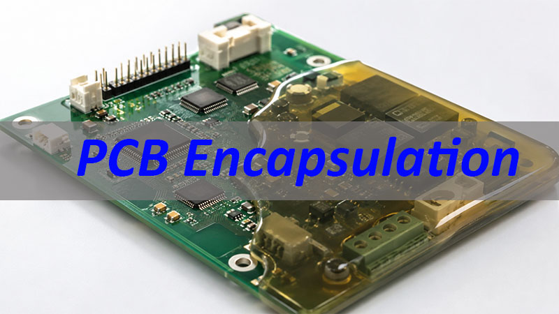
PCB encapsulation is the process of surrounding part or all of a printed circuit board with a protective material. This material may be epoxy, silicone, polyurethane, gel, or another electronic-grade compound. After curing, it forms a protective barrier around components, solder joints, copper traces, and exposed electrical areas.
The goal is simple: protect the circuit from the environment and help the product operate more reliably.
In practice, PCB encapsulation may be used for:
- Moisture protection
- Electrical insulation
- Mechanical support
- Shock and vibration resistance
- Corrosion prevention
- High-voltage spacing support
- Dust and chemical protection
- Added product durability
Unlike a simple enclosure, encapsulation directly surrounds the PCB and its components. This creates closer protection and can help reduce the risk of moisture, contamination, or physical stress reaching sensitive areas.
For example, an outdoor LED driver, a sensor module, or a power control PCB may use encapsulation to support stable performance in humid, dusty, or high-vibration working conditions.
What Is an Encapsulated PCB?
An encapsulated PCB is a circuit board that has been covered or surrounded by protective compound after assembly. The encapsulation may cover the whole board or only selected parts of the circuit.
There are several common forms:
| Type | Description | Common Use |
|---|---|---|
| Full board encapsulation | The whole PCB is covered by compound | Outdoor electronics, power modules, industrial boards |
| Partial encapsulation | Only selected areas are protected | High-voltage zones, connectors, sensor sections |
| Component-level encapsulation | Specific components are covered | Coils, transformers, ICs, fragile solder joints |
| Gel encapsulation | A soft gel protects the circuit | Sensors, delicate electronics, rework-sensitive boards |
| Potting-style encapsulation | The PCB is placed in a housing and filled with compound | LED drivers, power supplies, automotive modules |
An encapsulated PCB is often used when the board must work in a controlled and protected condition for a long service life. The final result depends on the board design, compound selection, curing process, component compatibility, and production control.
A good encapsulation design starts before manufacturing. Engineers should consider component height, connector access, heat dissipation, test points, repair needs, and the working environment before the board enters production.
How Does PCB Encapsulation Protect Electronic Circuits?
PCB encapsulation protects a circuit board by forming a physical and electrical barrier around the assembled board. This barrier helps reduce direct contact between the circuit and external stress.
- Moisture protection is one of the main reasons engineers use encapsulation. In humid environments, water vapor can enter small gaps around components and solder joints. Over time, this may affect insulation resistance and accelerate corrosion. A suitable encapsulant helps reduce moisture access and supports stable electrical behavior.
- Mechanical protection is also important. In products exposed to vibration or movement, components may experience stress from repeated motion. Encapsulation can help hold components in place and reduce the impact of vibration on solder joints.
- Electrical insulation is another key benefit. In high-voltage or power electronics, encapsulation can help increase insulation between conductive areas. This is especially useful when spacing is limited or when the assembly needs added protection from dust, humidity, or contamination.
- Chemical and dust protection is valuable in industrial environments. Encapsulation helps shield the PCB from particles, oil mist, cleaning agents, salt, and mild chemical exposure.
- Thermal support can also be part of the design. Some encapsulation materials are thermally conductive. They help transfer heat away from hot components while still offering electrical insulation. This is useful for LED drivers, power converters, battery-related electronics, and high-current control boards.
However, encapsulation should be selected carefully. A material that works well for one product may not be suitable for another. The right choice depends on thermal needs, hardness, rework requirements, voltage level, operating temperature, and environmental exposure.
PCB Potting Encapsulation vs Conformal Coating: What Is the Difference?
PCB encapsulation and conformal coating are both used to protect circuit boards, but they are not the same.
- Conformal coating is a thin protective film applied to the PCB surface. It follows the shape of the board and components, but it does not fully surround the board with a thick protective mass.
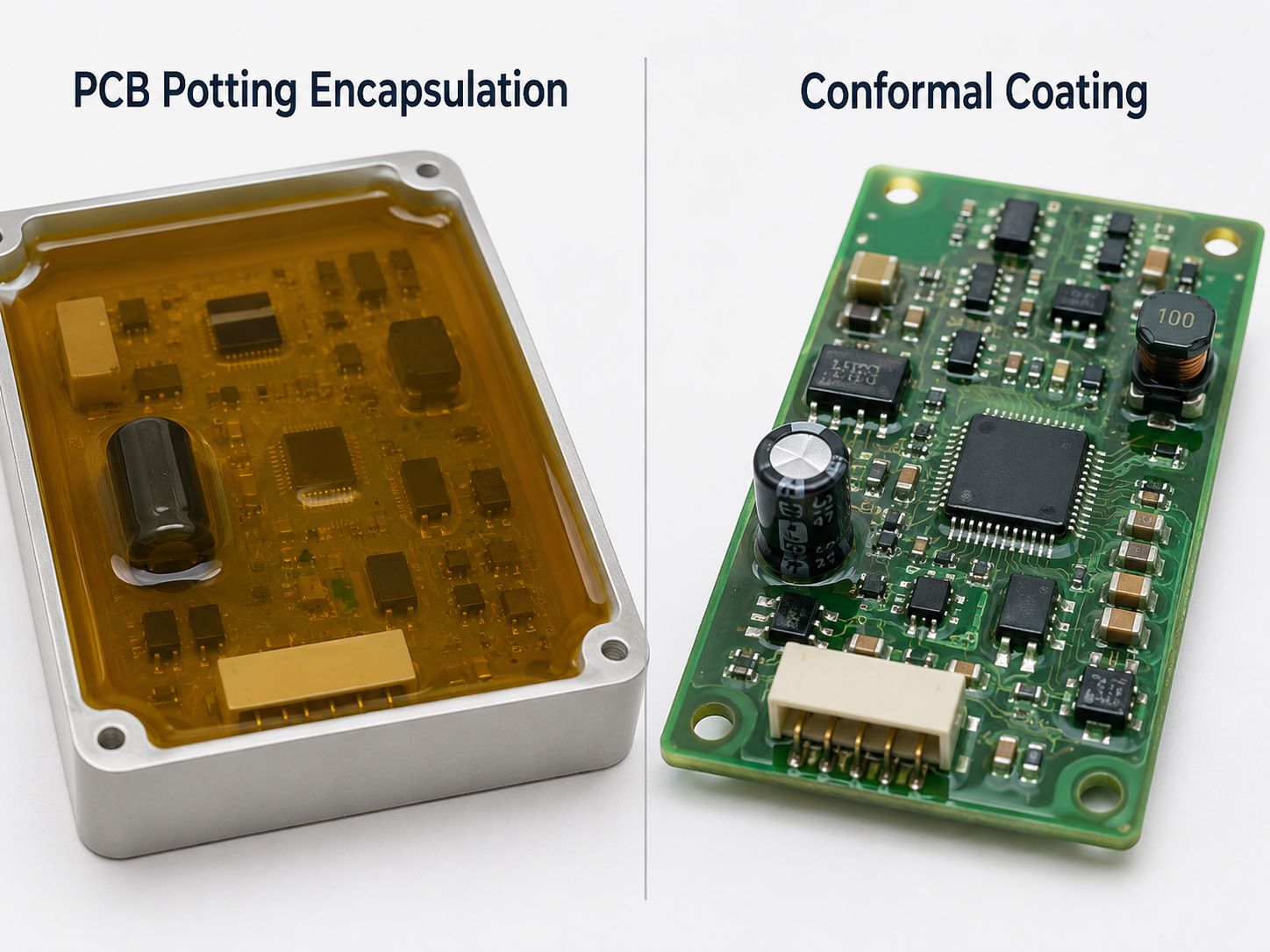
- PCB potting encapsulation is usually thicker and more protective. In many cases, the PCB is placed inside a housing, and liquid compound is poured into the cavity. After curing, the compound surrounds the board and components.
| Item | PCB Encapsulation / Potting | Conformal Coating |
|---|---|---|
| Thickness | Usually thicker | Usually thin |
| Protection level | Higher mechanical and environmental protection | Good surface-level protection |
| Moisture resistance | Strong, depending on material | Good for many normal environments |
| Vibration support | Better component support | Limited mechanical support |
| Rework | More difficult, especially with hard epoxy | Easier than full encapsulation |
| Weight | Adds more weight | Adds little weight |
| Cost | Often higher due to material and process | Usually lower |
| Common use | Outdoor, industrial, automotive, power modules | Consumer electronics, general PCBA protection |
Both methods are useful. The better choice depends on the final product.
Use conformal coating when the board needs light environmental protection, easier inspection, and better repair access. Use encapsulation when the PCB must handle stronger moisture, vibration, shock, dust, or electrical insulation requirements.
In some products, both methods may be considered during the design stage, but the final decision should be based on testing and working conditions.
What Materials Are Used for PCB Encapsulation?
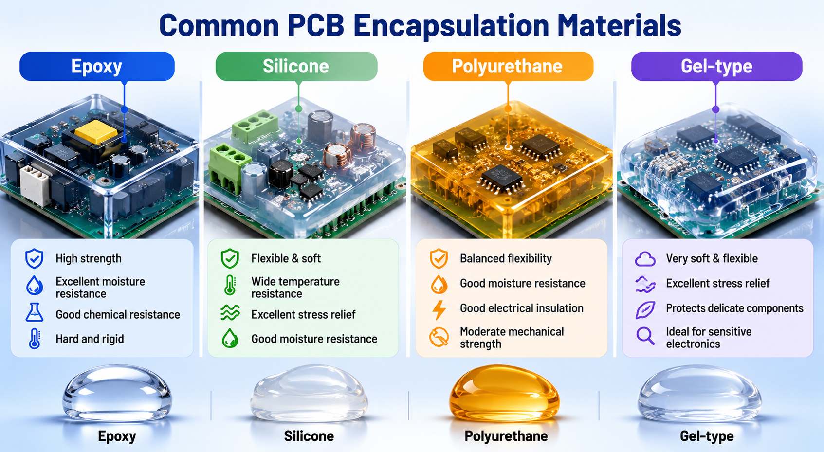
The most common PCB encapsulation materials include epoxy, silicone, polyurethane, and gel-type compounds. Each material has its own performance profile.
| Material | Main Features | Common Applications |
|---|---|---|
| Epoxy | Hard, strong, good chemical resistance, strong adhesion | Power modules, industrial electronics, high-protection assemblies |
| Silicone | Flexible, good temperature resistance, good stress relief | Automotive, LED lighting, sensors, outdoor electronics |
| Polyurethane | Balanced flexibility, moisture resistance, good electrical insulation | Industrial control, consumer electronics, low-to-medium stress environments |
| Silicone gel | Soft, flexible, easier stress relief | Sensors, delicate circuits, modules needing softer protection |
| Thermally conductive resin | Helps transfer heat while insulating electrically | LED drivers, power electronics, high-current boards |
- Epoxy for PCB encapsulation is widely used when the product needs strong mechanical protection and a hard finished structure. It bonds well and offers good resistance to moisture and chemicals. It is suitable for products where rework is not expected.
- Silicone encapsulation is preferred when flexibility and temperature cycling are important. Silicone can absorb stress better than many hard materials, making it useful for products exposed to expansion, contraction, or vibration.
- Polyurethane encapsulation offers a balanced option. It is softer than epoxy and can provide good moisture protection. It is often used when the board needs protection but also some flexibility.
- PCB encapsulation gel is useful for sensitive electronics. It is soft and can help protect components without placing heavy stress on fragile solder joints or delicate parts.
The best material is not chosen by name alone. Engineers should check hardness, viscosity, curing time, thermal conductivity, dielectric strength, adhesion, flame rating, operating temperature, and compatibility with components.
Is PCB Encapsulation Epoxy the Right Choice?
PCB encapsulation epoxy is a strong option for many electronic assemblies, especially when the board needs firm mechanical support and long-term protection.
Epoxy is often selected because it cures into a hard, durable material. It can protect the PCB from moisture, dust, shock, and chemical exposure. It also provides good electrical insulation, which is useful for power electronics and high-voltage applications.
Epoxy may be a good choice for:
- Power supply modules
- Industrial control boards
- LED driver boards
- High-voltage PCB assemblies
- Automotive control modules
- Outdoor electronic devices
- Products that do not require frequent repair
There are also design points to review. Because epoxy becomes hard after curing, it may create stress on components during temperature changes. For boards with tall components, fragile packages, ceramic parts, or fine solder joints, engineers should check whether a softer material is better.
Rework is another practical point. Once epoxy is fully cured, removing it can be difficult. For prototypes or products that may need repair, silicone or gel-type materials may offer better access.
In short, epoxy is a good choice when strength, insulation, and environmental protection are the main priorities. For high thermal cycling or rework-sensitive designs, another encapsulant may be more suitable.
What Are the Common PCB Encapsulation Methods?
PCB encapsulation can be done in several ways. The method depends on the product structure, protection area, material type, and production volume.
Full potting method
- The PCB is placed inside a housing or mold, and the compound is poured until the board is fully covered. This method is common for power supplies, LED drivers, outdoor modules, and automotive electronics.
Partial encapsulation method
- Only specific areas are covered. This is useful when connectors, test points, switches, or adjustment parts must remain accessible. It also helps reduce material cost and weight.
Dam-and-fill method
- A thicker material is used to create a border around the area, then a lower-viscosity compound fills the center. This method is often used when a controlled encapsulation area is needed.
Low-pressure encapsulation
- This method uses controlled pressure to apply material around the PCB or components. It is useful for delicate assemblies because it reduces mechanical stress during processing.
Gel encapsulation method
- A soft gel is applied around the circuit. This is common for sensor modules and assemblies that need protection with less mechanical stress.
A typical PCB encapsulation process includes:
- PCB assembly and inspection
- Cleaning or surface preparation if required
- Masking connectors, test points, or keep-out areas
- Mixing the encapsulation compound
- Dispensing or pouring the material
- Vacuum degassing when needed
- Curing under controlled conditions
- Final inspection and electrical testing
Process control is important. Air bubbles, poor adhesion, incorrect mixing ratio, incomplete curing, or material overflow can affect reliability. For production-quality PCBA, encapsulation should be treated as an engineered process, not only a simple filling step.
How to Choose Reliable PCB Encapsulation Services?
Choosing reliable PCB encapsulation services requires more than checking whether a supplier can pour resin onto a board. The supplier should understand PCB design, PCBA assembly, material behavior, testing, and end-use conditions.
A reliable manufacturing partner should review the project before production. This includes checking the Gerber files, BOM, assembly drawings, enclosure structure, component layout, connector positions, and the expected working environment.
Key points to evaluate include:
- Experience with PCB fabrication and PCBA assembly
- Understanding of epoxy, silicone, polyurethane, and gel materials
- DFM support before production
- Ability to protect connectors, test points, and functional areas
- Controlled dispensing, curing, and inspection process
- Electrical testing after encapsulation
- Support for prototypes, medium-volume builds, and mass production
- Traceability for materials, batches, and production records
- Knowledge of thermal, insulation, and reliability requirements
For many projects, the best result comes from early collaboration. If encapsulation is considered only after the PCB layout is finished, there may be less space for material flow, test access, heat transfer, or connector protection.
EBest Circuit supports customers with PCB fabrication, PCBA assembly, component sourcing, DFM review, testing, and production-quality support. For products that require protective assembly solutions, our engineering team can review the PCB layout, component structure, working environment, and assembly requirements before production.
If your project involves industrial control boards, LED drivers, automotive electronics, outdoor modules, power electronics, or other protected PCB assemblies, you can send your Gerber files, BOM, drawings, and requirements to sales@bestpcbs.com for engineering review and quotation.
FAQs About PCB Encapsulation
Q1: What is PCB encapsulation used for?
A1: PCB encapsulation is used to protect circuit boards from moisture, dust, vibration, chemicals, corrosion, and electrical stress. It is especially useful for outdoor electronics, industrial control boards, power modules, LED drivers, automotive electronics, and high-voltage assemblies.
Q2: Is PCB encapsulation the same as potting?
A2: They are closely related, but not always identical. Potting usually means placing the PCB inside a housing and filling it with compound. Encapsulation can also mean covering only part of a circuit board or selected components. In many PCBA projects, potting is one common form of PCB encapsulation.
Q3: What is the best material for PCB encapsulation?
A3: There is no single best material for every design. Epoxy is strong and durable. Silicone is flexible and suitable for temperature cycling. Polyurethane offers balanced protection. Gel is softer and suitable for delicate electronics. The best choice depends on temperature, vibration, moisture, voltage, heat dissipation, and rework requirements.
Q4: Can an encapsulated PCB be repaired?
A4: It depends on the material. Hard epoxy is difficult to remove after curing, while silicone or gel materials may be easier to handle. If rework is important, the material should be selected during the design stage, not after production starts.
Q5: Does PCB encapsulation help with waterproofing?
A5: PCB encapsulation can greatly improve moisture resistance when the right compound and process are used. However, waterproof performance also depends on the enclosure, connectors, cable exits, sealing design, and testing method. For outdoor or wet environments, the full product structure should be reviewed together.
Q6: Does encapsulation affect heat dissipation?
A6: Yes, it can. Some compounds trap heat, while thermally conductive materials can help transfer heat away from components. For power electronics, LED drivers, and high-current boards, thermal performance should be checked before choosing the encapsulant.
Q7: What should be checked before encapsulating a PCB?
A7: Engineers should check material compatibility, component height, connector access, test points, curing temperature, thermal needs, voltage spacing, and possible rework requirements. A DFM review before production helps avoid practical assembly problems.
Q8: When should I choose PCB encapsulation instead of conformal coating?
A8: Choose encapsulation when the board needs stronger protection against moisture, vibration, shock, dust, or electrical stress. Choose conformal coating when the board needs lighter protection and easier repair access. For harsh environments, encapsulation usually offers a higher protection level.
To conclude, PCB encapsulation is a practical way to improve circuit board durability in demanding applications. It protects assembled boards from moisture, vibration, dust, chemicals, corrosion, and electrical stress while supporting longer product life.
The right solution depends on the material, process, PCB layout, component structure, environment, and testing requirements. Epoxy, silicone, polyurethane, and gel materials all have useful roles, but they should be selected according to the actual product—not only by cost or habit.
Need support for a protected PCB or PCBA project? Pls feel free to send your Gerber files, BOM, drawings, and working environment requirements to sales@bestpcbs.com. EBest Circuit can support PCB fabrication, component sourcing, PCBA assembly, DFM review, testing, and production-ready manufacturing for encapsulated electronic assemblies.
You may also like


Tags: Circuit Board Protection, PCB Encapsulation, PCB Potting Materials