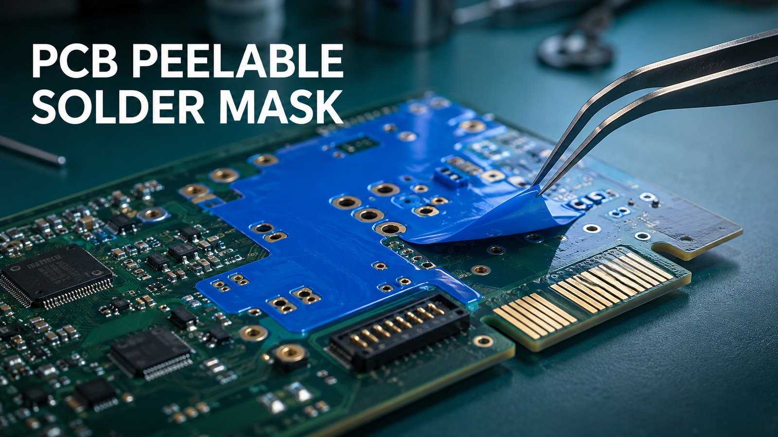
PCB peelable solder mask is a temporary masking material used to keep solder, flux, cleaning fluid or conformal coating away from selected holes, contacts and component areas. Unlike the permanent solder mask that remains on a finished PCB, the temporary film is applied for a defined process step and peeled away afterward.
It is useful only when the material, coverage, cure condition and removal plan match the assembly process. A vague fabrication note such as “add blue mask” is not enough: the supplier needs a marked layer, the protected features, the process exposure and the acceptance condition. This guide explains how to make that decision and prepare a quote-ready package.
What Is PCB Peelable Solder Mask?
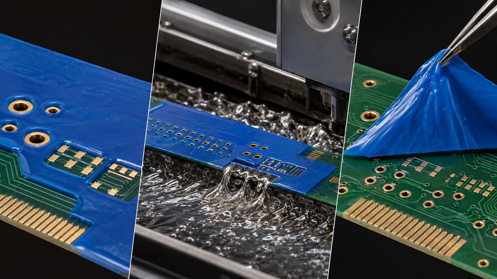
Peelable mask is a removable process aid, not the PCB’s permanent dielectric coating. It is commonly supplied as a viscous liquid that is placed over selected areas, cured into a flexible film, exposed to the intended process and removed manually. Product chemistry and processing windows differ, so the selected material’s current technical data sheet controls.
The distinction matters at purchase order review. IPC-SM-840 addresses permanent solder mask and flexible cover materials; it should not be used as a blanket qualification statement for every temporary peelable compound. Define temporary masking as its own fabrication or assembly requirement, with a named purpose and an agreed acceptance check.
| Layer or material | Purpose | End condition |
| Permanent solder mask | Insulates and protects the finished PCB surface while exposing intended pads | Remains on the board |
| Peelable temporary mask | Blocks solder, flux or coating from selected zones during a process step | Removed after the defined operation |
| Coverlay | Protects flexible-circuit conductors and defines openings | Remains as part of the FPC |
| Assembly tape or fixture | Provides temporary mechanical masking or support | Removed or reused according to the process |
When Should You Use Peelable Mask on a PCB?
Use it when selected features must stay free of solder or coating while nearby areas go through the same operation. The strongest use cases have a clear protected zone, a compatible material and an accessible peel path.
- Keep selected plated through-holes open during wave soldering for a later connector or mechanical assembly.
- Protect edge contacts, test points, pins or terminals from solder contact.
- Mask connectors and keep-out areas during spray, brush or dip conformal coating when the chosen product supports that exposure.
- Temporarily cover a local area during cleaning or another documented assembly operation.
- Reduce manual taping where repeatable dispensed or screened coverage is practical.
Do not choose it merely because it is removable. Very small, tightly packed or inaccessible zones may be difficult to coat consistently and harder to peel without fragments. High-temperature dwell, aggressive chemicals, bare-metal compatibility and cleanliness requirements must be checked against the exact product and process.
Peelable Mask vs Tape, Washable Mask and Permanent Solder Mask
The best option is the one that protects the feature through the process and can be removed without creating a new defect. Geometry, volume, temperature, chemistry and cleanliness usually decide the choice.
| Option | Good fit | Risk to check |
| Peelable mask | Irregular groups of holes or contacts; repeatable local coverage | Minimum film body, complete cure, peel access and fragment control |
| High-temperature tape | Simple edges or flat shapes; low-volume manual work | Labor, edge leakage, adhesive residue and placement variation |
| Washable mask | Processes with a validated compatible wash step | Complete dissolution, wash chemistry and trapped residue |
| Reusable fixture or pallet | Stable, repeated production with suitable board geometry | Tooling cost, board support, clearances and revision control |
| Permanent solder mask | Normal long-term surface protection and pad definition | It cannot serve as a removable post-process mask |
For a related overview of surface-protection choices, see the guide to solder mask on a PCB. For board purchasing, the broader PCB fabrication specifications checklist helps connect the mask note to the full build package.
Which PCB Areas Should Be Protected?
Mark only the features that must remain untouched by the next operation, then include enough surrounding area to form a continuous removable film. Protection zones often include through-holes reserved for a later insertion step, gold fingers, connectors, test points, terminals or coating keep-outs.
Review the zone against both sides of the board. A mask covering a hole on one side may not prevent ingress from the opposite side unless the application method and coverage are designed for it. Also check nearby solder joints, small components and board edges so the cured film can be gripped and peeled without stressing hardware.
- Identify the exact process the area must survive.
- Mark every protected feature on a dedicated drawing or unambiguous data layer.
- Define which board side receives the mask.
- Provide a clear boundary and any critical keep-out around adjacent pads or components.
- Confirm that the cured film has an accessible removal edge.
How Do Wave Soldering, Cleaning and Conformal Coating Affect the Choice?
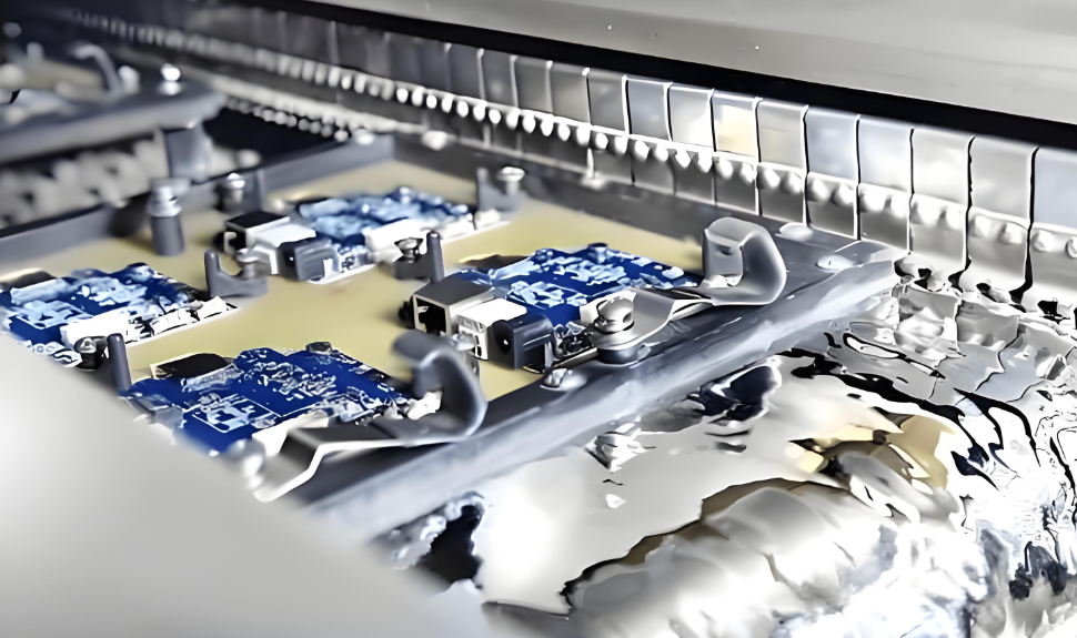
A peelable mask must be selected for the complete exposure sequence, not for temperature alone. During wave soldering it may encounter preheat, flux, molten solder and cleaning. During conformal coating it may contact solvent or water-based chemistry and must resist coating ingress around the protected feature.
Manufacturer data illustrates why a generic number is risky. Techspray’s WonderMASK P documentation gives product-specific cure, thickness and wave-solder limits, while MG Chemicals 862 lists its own application and cure parameters. Those values describe those named products; they are not universal PCB design rules. The contract manufacturer must confirm the actual material, application method and validated process window.
Surface finish also matters because the protected feature may be bare copper, plated metal, a soldered surface or a gold contact. Request compatibility confirmation for the actual finish rather than assuming all peelable masks behave alike. The selection of the exposed finish itself can be reviewed separately in the PCB surface-finish selection guide.
How Should Peelable Solder Mask Be Shown in Gerber Data and Drawings?
Create a dedicated, clearly named temporary-mask layer and repeat its purpose in the fabrication or assembly drawing. Do not rely on color alone, a screenshot or a filename such as “blue glue” without a legend. The manufacturer must know whether filled shapes indicate covered areas or openings.
- Name the layer, for example, TOP_PEELABLE_MASK or BOTTOM_TEMP_MASK.
- State the polarity: “filled geometry equals mask coverage.”
- Identify the operation: wave solder protection, conformal-coating keep-out or another defined step.
- Call out the board side, protected feature and any critical boundary tolerance.
- State that the mask is temporary and must be removed after the specified operation.
- Define the post-removal acceptance condition: no unintended solder/coating on protected features, no visible mask fragments, and no damage to pads, finish or components.
Include a reference image only as a communication aid; released manufacturing data must remain authoritative. If Gerber naming or polarity is unclear, expect a DFM question before production.
Which Material and Process Limits Must the Supplier Confirm?
Ask the supplier to identify the exact temporary mask and confirm it against the board finish and assembly route. Evidence should be marked as verified, to be confirmed or unavailable. Do not turn an open capability question into a public claim.
- Product name, revision of technical data sheet and shelf-life control.
- Compatibility with copper, gold, silver, solder, OSP or other exposed finish in the protected zone.
- Application method: hand dispense, template, pneumatic or robotic placement.
- Target film build and minimum practical geometry for a continuous peel.
- Cure condition, maximum process temperature and exposure time.
- Resistance to the actual flux, cleaner and conformal-coating chemistry.
- Removal method, peel access and residue/fragment inspection.
- First-article evidence before volume production.
For quotation, treat this as a capability-to-be-confirmed item. Board type, factory route, selected material and the original process record must all be checked before a supplier commits to a production value.
What Causes Lifting, Leakage, Tearing or Residue?
Most failures trace to surface condition, weak geometry, incomplete or excessive cure, incompatible chemistry or an uncontrolled removal step. Diagnose the mechanism instead of simply adding more material.
| Symptom | Likely questions | Control |
| Edge lifting | Was the surface contaminated? Was the film fully formed at the edge? | Clean surface, validate application and inspect before exposure |
| Solder or coating leakage | Was the boundary continuous? Did the process attack the mask? | Confirm coverage and chemistry with a first article |
| Film tears during peeling | Was it too thin, over-cured or trapped around geometry? | Use a validated film body and accessible peel path |
| Fragments remain in holes | Were holes bridged or filled in a way that prevents one-piece removal? | Inspect both sides and use magnification where needed |
| Residue or finish change | Is the exact material compatible with the surface and cleaner? | Approve the named material and verify after removal |
A preproduction board is valuable when the geometry is new, the protected finish is sensitive or the mask will see multiple chemical steps. Record the applied condition and removal result so production is not dependent on operator memory.
How Should Peelable Mask Be Inspected and Removed?
Inspect coverage before the protected operation and inspect cleanliness and feature condition after removal. The film should be removed using the method approved for the material, typically with a controlled manual peel. Do not assume a peelable mask will dissolve in the cleaning process.
- Before processing: verify the correct board side, all marked zones, continuous edges and no interference with intended solder joints.
- After processing: allow the board and coating, where applicable, to reach the approved removal condition.
- Peel without levering against small components, pads or fragile flex areas.
- Inspect holes, corners and narrow gaps for remnants.
- Verify protected contacts remain free of unintended solder or coating.
- Check that the surface finish, permanent solder mask and nearby components are undamaged.
- Record first-article photographs when the mask is a critical process characteristic.
If the user intent is specifically “how to remove solder mask from PCB,” first distinguish temporary peelable mask from permanent LPI solder mask. Permanent solder mask removal is a different rework operation and may damage copper or change the board’s insulation and reliability.
What Changes Peelable-Mask Cost and Lead Time?
Cost is driven mainly by protected-area complexity, application method, inspection effort and whether the process is already validated. A few accessible holes may be straightforward; many small islands, both-side coverage, tight component clearances or repeated coat/cure cycles add labor and risk.
Lead time can increase when the material must be sourced, the drawing is ambiguous, a first article is required, or compatibility testing is needed for a special finish, cleaner or coating. Quantity changes the economic choice: manual masking can fit prototypes, while recurring production may justify a template, controlled dispensing program or solder pallet.
Ask suppliers to separate non-recurring setup from per-board masking and inspection. That makes quote comparisons more meaningful than a single total price with different assumptions hidden inside it.
What Should You Send in a Peelable-Mask RFQ?
A quote-ready package tells the supplier what to protect, what the mask must survive and how the result will be accepted. Send:
- Gerber or ODB++ files, drill data and fabrication drawing.
- A dedicated top and/or bottom temporary-mask layer with stated polarity.
- PCB stackup, material, thickness, copper and surface finish.
- Assembly drawing, BOM and CPL when the board will also be assembled.
- Wave-solder profile or other expected temperature exposure.
- Flux, cleaning and conformal-coating details where relevant.
- Quantity, prototype/production stage and target delivery date.
- Required first-article photographs, inspection report or sample approval.
- Post-removal acceptance criteria and any cleanliness requirement.
For a complete manufacturing handoff, pair this with the site’s PCB DFM guide. A supplier can then review mask feasibility together with the board outline, holes, finish, assembly sequence and inspection plan.
FAQ About PCB Peelable Solder Mask
Is peelable solder mask permanent?
No. It is a temporary process material intended to be removed after the specified soldering, cleaning or coating operation. Permanent PCB solder mask remains on the finished board.
Why is peelable solder mask often blue or pink?
Color helps operators see coverage and, for some products, may indicate curing progress. Color alone does not identify chemistry or performance, so use the product name and current TDS.
Can peelable mask protect plated through-holes during wave soldering?
Yes, this is a common application when the selected product and coverage are validated for the wave process. Both-side access, film continuity and post-process removal still require review.
Can it protect gold fingers and contacts?
Some named products are documented for contacts or gold fingers, but compatibility must be confirmed for the exact finish, material and exposure sequence.
Is peelable mask the same as coverlay?
No. Coverlay is a permanent protective layer used on flexible circuits. Peelable mask is temporary and is removed after its process function is complete.
Can I specify only “blue mask” on the drawing?
No. State that it is temporary peelable mask, define the covered geometry and polarity, identify the board side and operation, and specify removal and acceptance requirements.
How thick should peelable solder mask be?
There is no single universal value. Each material has a product-specific recommended film build, and the practical geometry also depends on application and removal. Use the selected product’s TDS and supplier approval.
Does peelable mask leave residue?
A suitable, correctly processed product is intended to remove cleanly, but residue or fragments can occur if chemistry, cure, surface condition or geometry is wrong. Post-removal inspection is necessary.
How is temporary peelable mask removed from a PCB?
After the approved process and cooling or coating condition, it is normally lifted and peeled manually according to the material instructions. Inspect holes and tight corners for remnants.
Should the first production build include a mask sample?
Yes when the geometry, finish, chemistry or thermal route is new or critical. A first article can confirm coverage, survival, removal and the protected-feature acceptance condition before volume production.
Need a PCB quote with temporary peelable masking?
Send EBest Circuit your Gerber/ODB++ files, peelable-mask layer, surface finish, process profile, quantity and acceptance requirements. We will review the data and confirm the applicable manufacturing route before quotation.