PCB manufacturing PCB manufacturing
Home > Blog

PCB Drilling

PCB Hole Size Tolerance: PTH, NPTH, and Press-Fit Guide
Saturday, September 5th, 2026
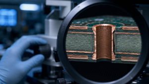
PCB quality engineer measuring finished hole size with optical equipment and pin gauges
Finished-hole tolerance must match the hole function, plating condition and agreed measurement method.

PCB hole size tolerance defines the acceptable range of the finished hole, not simply the diameter of the drill tool. Plated through holes (PTH), non-plated holes (NPTH), vias and press-fit holes serve different functions, so one blanket tolerance rarely produces the best balance of fit, reliability, yield and cost.

The drawing should state whether each dimension is finished or drilled, whether plating is present, what feature mates with the hole, and how acceptance will be measured. Without those details, a supplier may meet a numerical callout while missing the assembly requirement.

What PCB Hole Size Tolerance Actually Controls

A tolerance controls the allowed upper and lower finished diameter for a defined hole class. It protects lead insertion, fastener fit, press-fit retention, plating reliability or via geometry. The tolerance should be derived from that function.

A nominal value alone is incomplete. A drawing needs a plus/minus or limit range, the plated status and any positional or geometric requirement that affects fit.

Drill Tool Size vs Finished Hole Size

Mechanical drill diameter is a manufacturing input; finished hole diameter is the inspected output. For a PTH, copper deposition reduces the open diameter after drilling. Cleaning, desmear, plating distribution and measurement method affect the final result.

NPTH features normally do not receive barrel copper, but routing/drilling variation, material behavior and finishing still matter. Do not copy a finished size into the drill file and assume the fabricator will interpret the required allowance.

How PTH and NPTH Hole Tolerances Differ

Hole class Primary function Tolerance evidence
PTH component hole Lead insertion plus reliable plated connection Finished diameter, plating and lead envelope
Via Electrical interconnection Finished hole, aspect ratio, annular ring and plating
NPTH mounting hole Mechanical clearance or location Finished diameter, position and mating hardware
Press-fit hole Controlled interference with compliant pin Connector specification, finished diameter and plating
Slot Tab, lead or mechanical feature Finished width/length, radii and plated status

Keep PTH and NPTH features separate in the drill data and drawing. Ambiguous mixed tables are a common source of quoting and production errors.

Why Press-Fit Holes Need a Functional Window

Press-fit performance depends on the relationship between the finished plated hole and the connector pin system. A hole that is too small may raise insertion force or damage the barrel; one that is too large may reduce retention or electrical contact.

Use the connector manufacturer’s approved finished-hole window and identify the pin part number. Align it with plating, board thickness, copper construction, insertion tooling and inspection. Our press-fit PCB assembly guide explains the broader process.

Need a hole table checked before PCB release?

Send the drill files, fabrication drawing, connector data, stackup and finished-hole requirements. EBest Circuit can flag ambiguous plated status and tolerance conflicts.

How Via Tolerance Interacts with Annular Ring

Finished-hole variation and positional variation both consume the copper land around a via. A larger finished diameter can reduce remaining annular ring even when the hole center is unchanged; registration shift can reduce it on one side.

Review pad diameter, finished hole, plating allowance, layer registration and breakout criteria together. See the annular ring guide and PCB aspect-ratio guide.
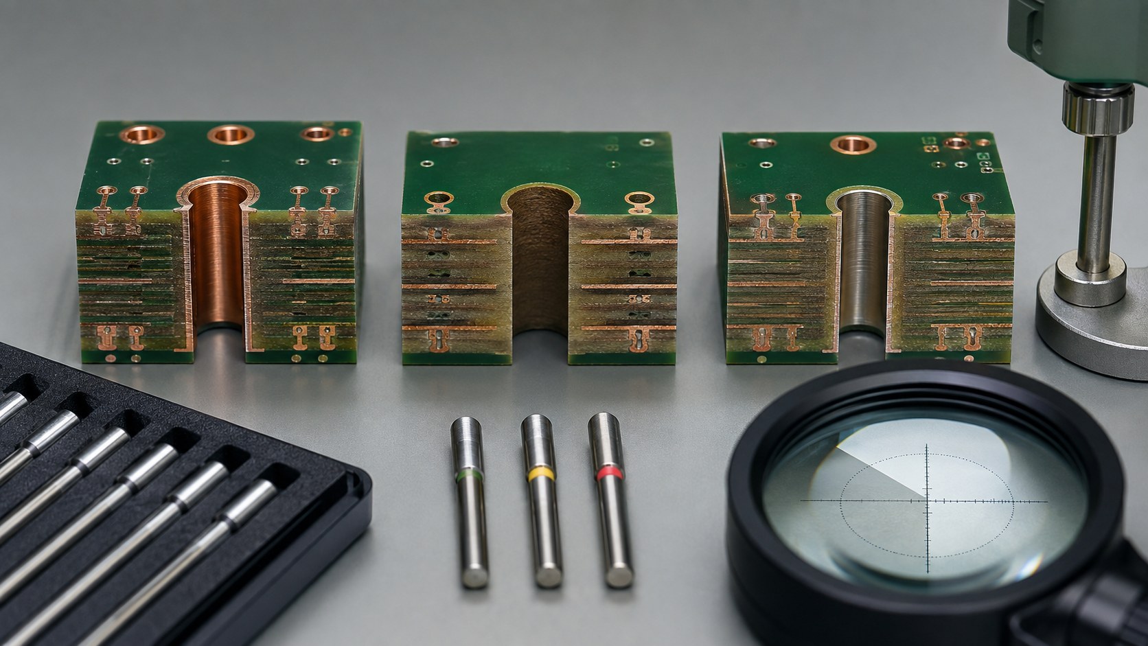
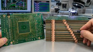
Cross-section samples comparing plated non-plated and press-fit PCB holes
PTH, NPTH and press-fit holes need different acceptance logic even when nominal diameters look similar.

Manufacturing Variables Behind Finished-Hole Variation

Finished size is influenced by more than tool diameter. Drill wear, runout, panel-stack setup, laminate movement, desmear, electroless copper, electrolytic plating and local current distribution can change the result.

  • Tool selection and wear influence the drilled opening.
  • Material and stack height affect drilling behavior.
  • Cleaning/desmear prepares the wall before metallization.
  • Barrel copper reduces the open diameter of plated holes.
  • Plating distribution can vary across a panel.
  • Final finish or secondary operations may alter particular features.

These variables explain why capability must be confirmed for the actual stackup and hole class, not copied from a generic tolerance table.

How Finished PCB Hole Size Is Measured

The measurement method must suit the hole and acceptance purpose. Pin gauges can quickly verify functional pass/fail windows; optical systems can measure diameter and location; cross-sections can show plating and wall condition.

Agree whether the reported result is a minimum diameter, maximum diameter, two-axis optical value or gauge acceptance. Sampling location and lot coverage also matter when plating varies across the panel.

Diameter tolerance must also be separated from positional tolerance. A hole can have the correct opening but sit too far from its datum, pad or mating feature. Conversely, a correctly located center can still fail a functional gauge because the finished opening is undersize. For slots, measure width, end radii, length and position according to the drawing rather than reducing the feature to one diameter.

Measurement timing should be clear. A result taken before plating does not prove the final PTH opening, while an inspection after an unapproved secondary operation may no longer represent the released process. Keep equipment calibration, sample identity and revision traceable to the production lot.

Why Over-Tight Tolerances Increase Cost and Risk

A tolerance tighter than the product needs can force special tooling, sorting, additional coupons, lower panel utilization or extra process controls. It may also reduce supplier options without improving assembly.

Classify holes by function. Apply tight limits only to features that require them, such as qualified press-fit systems or precision mechanical interfaces. Use the fabricator’s standard capability where it satisfies ordinary via or lead-clearance needs.

How to Build a Clear Hole and Slot Table

  1. Assign a unique class to each functional hole family.
  2. State PTH, NPTH or other required treatment.
  3. Specify finished size and tolerance or limit range.
  4. Identify quantity and associated drill-tool reference.
  5. Separate round holes from plated/non-plated slots.
  6. Call out press-fit part numbers and approved windows.
  7. State positional requirements where mechanical fit depends on them.
  8. Keep Gerber/ODB++, NC drill and drawing revisions synchronized.

For base size selection, review the protected standard PCB drill sizes guide.

Supplier Evidence and Nonconformance Review

Acceptance evidence should prove the required finished condition. Depending on risk, that can include first-piece measurements, gauge results, cross-sections, plating records, coordinate reports and lot traceability.

If a hole is out of tolerance, determine scope and function before disposition. Do not enlarge, replate or accept a critical feature without confirming its effect on annular ring, barrel copper, fit and reliability.

Comparing two PCB quotes with different hole assumptions?

Send both interpretations with the board files and mating-part data. We can help normalize finished-size, plating and inspection requirements.

PCB Hole Tolerance Decision Checklist

  • Is the value a drill size or finished size?
  • Is the feature plated, non-plated or press-fit?
  • What part, lead, pin or fastener must fit?
  • Does annular ring remain acceptable at worst case?
  • Are position and diameter tolerances separated?
  • Is the measurement method defined?
  • Are only functional holes tightly controlled?
  • Do all released files use the same revision?

What to Send for EBest Circuit Review and Quotation

Send Gerber or ODB++, NC drill data, fabrication drawing, stackup, materials, copper requirements, hole/slot table, connector or hardware specifications, quantities, assembly needs, inspection level and target delivery.

EBest Circuit can review data consistency and return questions before quotation. Specific tolerance capability must be confirmed against the selected construction and approved manufacturing route.

PCB Hole Size Tolerance FAQ

What is PCB hole size tolerance?

It is the allowed range around a defined finished or drilled hole dimension.

Is drill size the same as finished hole size?

No. Plating and other processing change the final opening, especially for PTH features.

Do PTH and NPTH holes use the same tolerance?

Not automatically. Their processes and functions differ, so they should be specified separately.

Why are press-fit holes more sensitive?

The finished plated diameter directly affects insertion force, retention and contact behavior.

How is a finished hole measured?

Common methods include calibrated pin gauges, optical measurement and cross-section analysis.

Does plating reduce hole diameter?

Yes. Barrel copper occupies part of the drilled opening, so fabrication compensates from the finished requirement.

Can a larger hole reduce annular ring?

Yes. Increasing the opening leaves less copper land around the hole.

Should every hole receive a tight tolerance?

No. Tighten only features whose fit or reliability requires it.

What causes hole-size variation?

Tool condition, drilling setup, material behavior, cleaning, plating and measurement all contribute.

What files prevent tolerance mistakes?

Provide synchronized artwork, NC drill files, a finished-hole table, stackup and mating-part specifications.

Make every critical hole measurable and manufacturable.

Send your PCB files, hole table, connector data, quantities and target delivery.

You may also like

PCB Drill Wander: Causes, Inspection, and Prevention
Saturday, September 5th, 2026
PCB engineer inspecting drilled-hole position and annular ring alignment
Drill-wander control combines machine, tool, panel-stack and design evidence rather than relying on a visual check alone.

PCB drill wander is unintended lateral movement of a mechanical drill as it enters and travels through a production panel. The finished hole can deviate from its programmed path, reducing annular ring, moving closer to internal copper or creating a non-straight hole wall.

An off-center hole is not automatically proof of drill wander. Image-to-drill registration, layer shift, artwork scaling and lamination movement can create a similar top-view result. A useful investigation separates the drill path from the copper-layer positions before selecting corrective action.

What PCB Drill Wander Means

A wandering drill does not follow the intended axis consistently through the panel stack. Deflection may begin at entry, grow with depth or change as the tool crosses different materials. The entry and exit locations can therefore tell only part of the story.

The risk rises when the hole is small relative to drilling depth, the stack is unstable, the tool is worn or running inaccurately, or feed/speed and chip removal are not suited to the construction.

Drill Wander vs Layer-to-Drill Registration Error

Drill wander describes the physical hole path; registration error describes the relationship between that path and copper features. A straight hole can look off-center if an inner layer shifted. A wandering hole can enter near center but approach an internal land at depth.

Observation Possible mechanism Evidence to review
Entry and exit displaced similarly Machine/program/panel registration Tool coordinates, targets and first-piece measurement
Hole path bends through depth Tool deflection or wander Cross-section and entry/exit comparison
Different inner layers show different land offset Layer registration or lamination movement Layer targets and coupon cross-section
Problem increases as a bit is used Wear, debris or runout Tool-life and spindle records

Why a PCB Drill Bit Deflects

The tool follows the combined mechanical forces at entry and throughout the cut. If those forces are uneven, a slender drill can bend away from the programmed axis.

  • Surface texture or unsuitable entry material can disturb initial centering.
  • Excess panel-stack height increases the unsupported cutting path.
  • Worn or damaged cutting edges create unequal load.
  • Spindle runout and poor collet condition move the tool off axis.
  • Incorrect feed, speed or retraction can increase heat and deflection.
  • Poor debris removal can recut chips and load the flutes.
  • Construction changes can alter cutting resistance through the stack.

Entry Material, Panel Stack, and Backer Control

The drill must enter cleanly, hold its path through every panel and exit without excessive burr or breakout. Entry and backing materials support those tasks, while stack height affects rigidity, heat and chip evacuation.

A production route should match the tool diameter and board construction. Increasing the number of panels per drill stack may improve throughput, but it also changes the path length and process margin. The qualified setup—not a universal stack count—should determine the limit.

Seeing reduced annular ring or unexplained hole offset?

Send the stackup, drill files, finished-hole requirements, copper images and inspection evidence. EBest Circuit can help separate design clearance from drilling and registration risk.

Tool Wear, Runout, and Drilling Parameters

Drill-condition controls should be tied to measured output. Tool-life limits, spindle maintenance, collet cleanliness and first-piece verification help keep a process stable, but the correct thresholds depend on the tool and construction.

Feed that is too aggressive can increase lateral force; an unsuitable speed can raise heat or wear. Slow is not automatically safe: rubbing rather than cutting can also damage the hole. Process engineers qualify the combination and monitor changes rather than adjusting one parameter in isolation.

How Laminate Construction and Hole Geometry Change the Risk

A hole must be evaluated against total drilling depth, material system, copper distribution and nearby features. Thick builds and small tools deserve additional review because stiffness and chip evacuation become more demanding.

Hole type also matters. Through holes, press-fit holes, component leads, vias and controlled-depth features have different finished-size and structural priorities. For size selection, see the standard PCB drill-size guide. Controlled-depth work is covered in our controlled-depth drilling guide.

Annular Ring and Hole-to-Copper Clearance Risks

Drill movement consumes the registration allowance built into pads and clearances. The critical question is the finished relationship at every connected and nonconnected layer—not whether the drill symbol was centered in CAD.

Possible results include reduced annular ring, tangency, breakout, unwanted approach to plane copper, or a weakened connection. Pad size should be reviewed with finished-hole tolerance, plating allowance and the fabricator’s registration capability. See the PCB annular ring guide for the geometry.

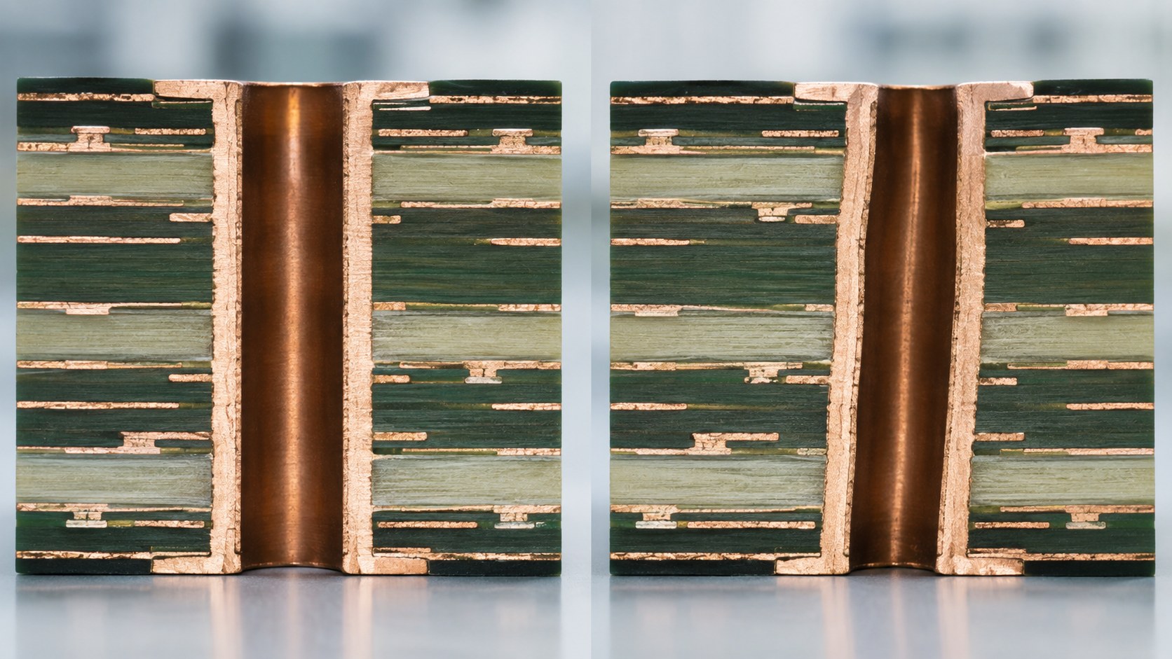
PCB cross-sections used to compare hole path and internal layer registration
Cross-sections help distinguish hole-path behavior from the position of individual internal copper layers.

Hole-Wall and Plating Consequences

A non-straight or rough drilled hole can complicate desmear, activation and copper deposition. Drill smear, debris, wall roughness or local geometry changes may affect how the plated barrel forms.

Do not assume every offset hole has a plating defect, and do not assume good continuity proves the complete wall is acceptable. Review hole-wall condition, copper coverage and connection geometry using the agreed acceptance plan.

How PCB Drill Wander Is Detected

Detection works best when top-view measurement is combined with depth-sensitive evidence. Automated optical inspection or coordinate measurement can find entry-position trends. Exit-side review can reveal accumulated deviation. Cross-sections show the path relative to inner lands and wall condition.

Coupon and panel mapping are important when a defect changes with machine position, stack location or tool life. Record the drill program, tool identity, hit count, panel stack and measurement location so the pattern can be reproduced.

DFM Actions Before PCB Release

  1. Define finished rather than only nominal drill sizes.
  2. Provide a clear plated/non-plated and tolerance table.
  3. Check pad and plane clearances at every layer.
  4. Flag press-fit, connector and other function-critical holes.
  5. Review small holes against the actual construction depth.
  6. Avoid ambiguous duplicate drill entries or mixed units.
  7. Confirm how controlled-depth or backdrilled features are identified.
  8. Request approval before any geometry change that affects function.

What to Ask After a Drill-Position Nonconformance

A corrective-action response should identify the mechanism, affected scope and evidence of containment. Ask whether the path wandered, copper layers shifted, the panel registered incorrectly, or several factors combined.

Useful evidence includes mapped measurements, cross-sections, tool-life data, spindle/collet checks, stack setup, entry/backer lot and first-piece records. The supplier should explain how affected inventory was identified and how the revised control will be verified.

Need evidence before accepting a drilled-hole deviation?

Share the drawing, photos, measurement report, cross-sections and lot history. We can help frame the containment and acceptance questions.

What to Send for EBest Circuit Drilling Review and Quotation

Send Gerber or ODB++, NC drill files, stackup, material and copper requirements, finished-hole table, tolerances, quantities, assembly requirements, test needs and target delivery. Identify press-fit and other critical holes and provide connector specifications when relevant.

EBest Circuit can review file consistency, pad/clearance relationships and drilling-risk questions before quotation. Specific drill, aspect-ratio or tolerance capability must be confirmed against the current construction and approved production route.

PCB Drill Wander FAQ

What is PCB drill wander?

It is unintended lateral deflection of a mechanical drill from its programmed axis as it enters or travels through a PCB production stack.

Is every off-center hole caused by drill wander?

No. Artwork, layer and drill registration errors can create a similar top-view appearance.

How does drill wander affect annular ring?

It moves the finished hole toward a pad edge, reducing the remaining copper land and potentially causing tangency or breakout.

Can a worn drill cause wandering?

Yes. Uneven wear or damage can increase lateral cutting forces, although the complete machine and setup should be investigated.

Does a taller panel stack increase risk?

It increases the drilling path and can reduce margin for small tools; the qualified stack limit depends on construction and process.

Can AOI detect drill wander?

Top-view inspection can reveal hole-to-pad offset trends, but cross-section or entry/exit evidence may be needed to prove path deflection.

Can electrical test find every drill-wander problem?

No. It can identify open/short conditions but may not fully characterize remaining land, hole-wall geometry or latent structural risk.

Should designers increase every via pad?

No. Pad changes consume routing space and should be based on the actual tolerance budget and functional requirements.

What records help identify the root cause?

Tool identity and hit count, spindle/collet checks, drill parameters, stack setup, panel mapping, targets and cross-sections are useful.

What files are needed for drilling DFM?

Provide artwork, NC drill data, stackup, hole table, tolerances, critical-hole notes, quantities and any applicable component specifications.

Protect annular ring and plated-hole reliability before production.

Send your board data, hole table, stackup, quantities and target delivery for a project-specific review.

You may also like

PCB Controlled Depth Drilling for Via-Stub Control and Reliable Fabrication
Saturday, September 5th, 2026
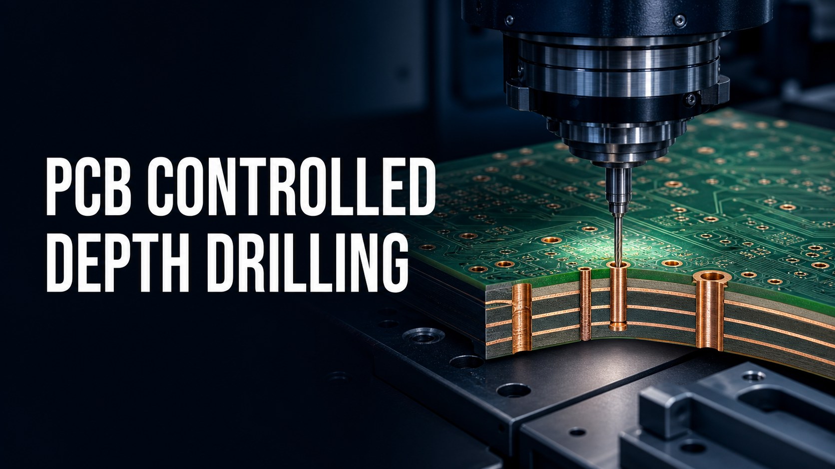
CNC spindle performing controlled depth drilling on a multilayer PCB cross-section
Controlled-depth drilling removes an unused plated via barrel only when the stackup, drill side and target layer are clearly defined.

PCB controlled depth drilling, commonly called backdrilling, removes the unused section of a plated through-hole barrel after the electrical connection layer. The remaining copper cylinder is a via stub. At high edge rates, that stub can behave as a resonant branch, increasing reflection, insertion loss or jitter.

Backdrilling is not a default requirement for every multilayer PCB. Use signal-integrity analysis to identify the vias that need it, then release exact drill side, target layer, hole group and inspection criteria to the fabricator. A note that only says “backdrill high-speed vias” is not manufacturable enough.

What Is PCB Controlled Depth Drilling?

Controlled-depth drilling is a secondary mechanical drilling operation that enters a plated hole from one board face and stops at a defined Z-depth. For via-stub removal, the secondary drill is larger than the finished plated hole so it removes unwanted copper barrel without creating a new electrical connection.

The active via section remains between the signal transition and the opposite required connection. The removed section becomes a non-plated cavity. Because the drill approaches a real copper layer, depth accuracy, registration and stackup thickness variation all matter.

“Controlled-depth drilling” can also describe other depth-limited machining. On a fabrication drawing, state that the feature is backdrilling for via-stub removal and define the layer pair. That prevents confusion with controlled-depth blind holes or mechanical recesses.

When Does a Via Stub Justify Backdrilling?

Backdrilling is justified when the predicted or measured channel penalty from the unused barrel exceeds the design budget and a simpler architecture cannot remove it. Data rate alone is an unreliable trigger because transition rise time, stub length, dielectric properties and channel topology interact.

  • Model the connector, package, trace, via transition and unused barrel together.
  • Check return loss, insertion loss and resonance over the required frequency range.
  • Identify only the nets whose stubs materially affect the channel.
  • Consider whether changing the signal layer, using a blind via or shortening the through connection solves the problem.
  • Confirm the improved design still meets power, mechanical, test and cost constraints.

Typical candidates include high-speed serial links, fast memory channels and dense connector fields. Low-speed controls and power vias usually do not need the same treatment unless analysis finds a specific issue.

Backdrilling vs Blind Vias, Microvias and Sequential Lamination

Choose the interconnect structure during stackup planning, not after routing is complete. Backdrilling preserves a through-hole manufacturing route while removing selected unused barrels. Blind or microvia structures avoid the long barrel by connecting fewer layers, but add their own build-up and reliability constraints.

Option Best fit Main tradeoff
Backdrilled through via High-layer board needing through-via routing with selected stub removal Secondary drilling, larger clearance and depth verification
Blind mechanical via Connection from a face to a defined internal layer Depth/aspect-ratio and lamination constraints
Laser microvia Short adjacent-layer HDI connections and fine-pitch escape Sequential build-up, stacking rules and qualification
Through via without backdrill Channels that tolerate the remaining stub Lowest process complexity but potential SI penalty

For structure selection, compare this guide with blind vias in HDI design, the broader PCB via types guide, and the HDI PCB fabrication guide when sequential structures are under review.

Which Vias Should Be Backdrilled?

Create an explicit backdrill set from the routed nets and stackup; do not select holes by diameter alone. Two identical through holes can require different treatment because their signal transitions end on different layers.

  • Identify the net and via designator or tool group.
  • Confirm the first and last electrically connected layers.
  • Determine whether the unused barrel is above, below or on both sides of the active connection.
  • Exclude component pins or vias whose barrel is still electrically required.
  • Check nearby copper, planes, anti-pads and adjacent holes against the larger backdrill.
  • Group only holes that share the same drill side, target layer and permitted depth window.

A separate table for each group is easier to inspect than one global note. If both sides are drilled, use distinct tool names and views.

How to Define Drill Side and Target Layer

Every controlled-depth drill group needs a physical entry side and an unambiguous stopping relationship to the last active layer. Layer names such as L10 are meaningful only when the controlled stackup revision is attached.

  1. Freeze the numbered stackup and identify top and bottom orientation.
  2. For each via, mark the signal transition and the unused barrel direction.
  3. Specify backdrill from top or bottom.
  4. State the last active layer and the layer the drill must not damage.
  5. Define the acceptable residual stub or depth window from SI and fabrication agreement.
  6. Assign a unique drill tool/group and include it in the drill legend.
  7. Cross-check the NC data, fabrication detail and net list before release.

Do not define only an absolute machine depth if the board thickness or stackup can change. Tie the requirement to the functional layer and let the approved manufacturing data translate it into the controlled drill depth.

How Much Residual Stub Is Acceptable?

Acceptable residual stub is a channel-design decision constrained by manufacturing depth tolerance. There is no universal value that fits every material, layer count, edge rate and loss budget.

A shorter stub generally moves its resonance higher and reduces its effect in the operating band, but demanding an unnecessarily small remainder can increase the risk of drilling into the capture layer or active connection. The specification needs margin for dielectric-thickness variation, copper thickness, lamination movement, drill setup and measurement uncertainty.

Use the SI model to set the maximum electrical remainder, then ask the fabricator for a safe production window. Record both the target and acceptance method. EBest-specific values are to be confirmed from the original factory capability data for the selected stackup.

How Backdrill Diameter Affects Pads and Clearances

The secondary drill is larger than the plated hole, so it consumes more radial space than the original via. Copper that was safe around a normal through hole may be cut or exposed by the backdrill.

  • Define the backdrill tool independently from the finished hole.
  • Check anti-pad clearance on every traversed layer.
  • Remove nonfunctional pads only through an approved stackup and fabricator rule.
  • Protect the required capture pad at the last active layer.
  • Review adjacent traces, plane islands, via pairs and connector pin fields.
  • Include drill wander and layer registration in the clearance analysis.

Do not copy a universal oversize. Drill diameter, plating, registration and breakout rules vary by build. Use a board-specific DFM check.

Why the Released Stackup Must Control the Backdrill

Backdrill depth is inseparable from the physical stackup. A change to prepreg thickness, core construction, copper weight or layer numbering can move the active layer relative to the board surface.

Use one revision-controlled stackup across CAD, SI analysis, fabrication drawing and NC drill output. If the fabricator proposes a material or thickness substitution, repeat the depth and residual-stub review before approval. A substitution acceptable for impedance may still change backdrill margin.

For broader release discipline, use the PCB DFM checklist. Backdrill should be part of the same controlled stackup review, not a note added after CAM preparation.

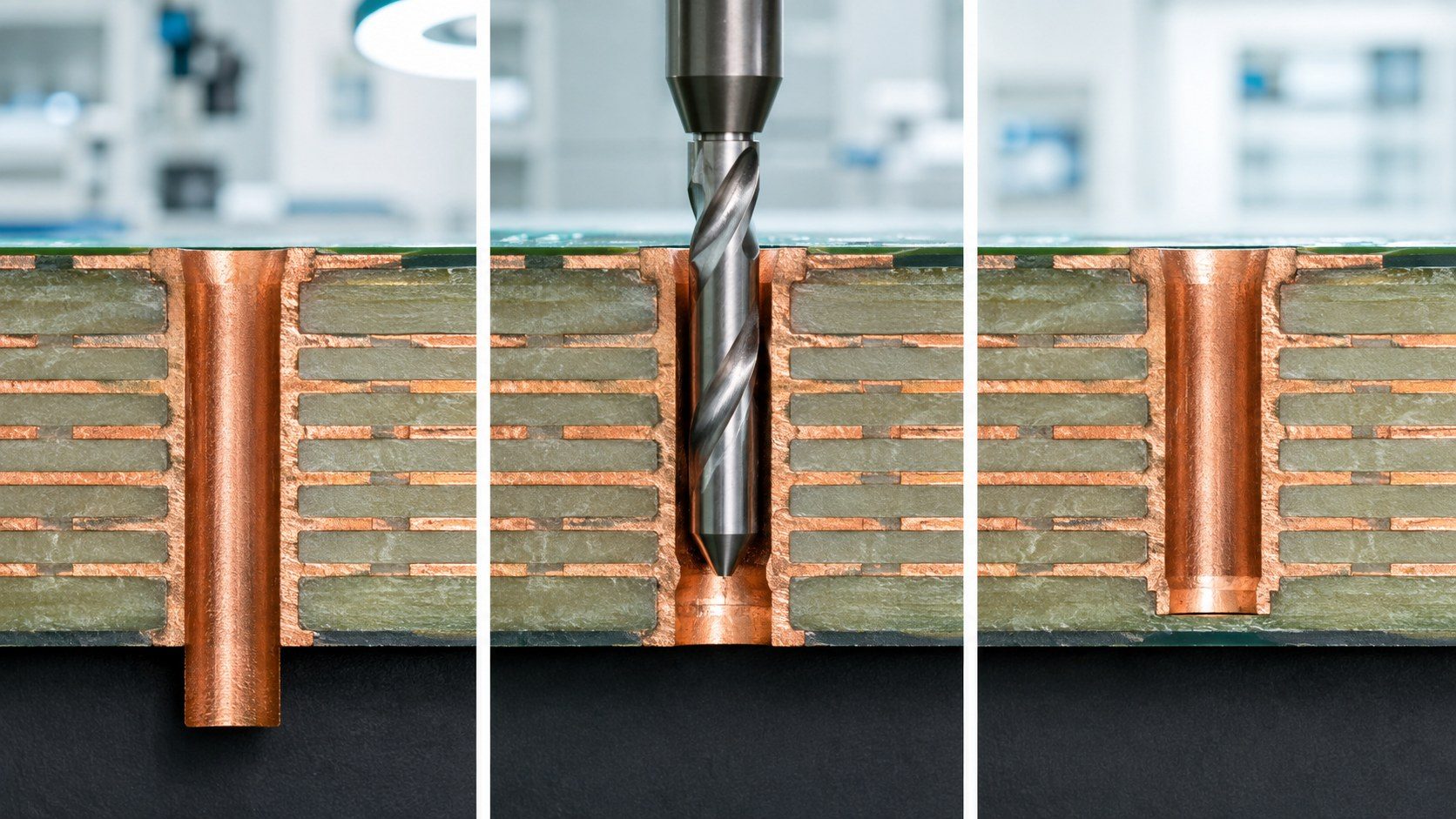
Before, drilling and after cross-sections of a plated PCB via stub removed by backdrilling
The secondary drill removes the unused barrel while leaving controlled separation from the last active connection.

What Gerber, Drill and Fabrication Notes Must Show

The released package should allow CAM to identify every backdrilled hole, its direction and its layer relationship without inference. Provide:

  1. A numbered, dimensioned stackup with material and finished thickness.
  2. Normal NC drill data and separate controlled-depth drill files or clearly identified tool groups.
  3. A backdrill table listing group, entry side, source hole/tool and last active layer.
  4. The agreed residual-stub or depth requirement and tolerance source.
  5. Backdrill diameter or a requirement for supplier calculation/approval.
  6. Cross-section details for top, bottom and double-sided cases.
  7. Inspection, coupon, microsection or depth-report requirements.
  8. A note that any stackup revision requires backdrill revalidation.

ODB++ or IPC-2581 may carry richer relationships, but a human-readable table remains valuable for quotation and independent review.

How Controlled Depth Drilling Is Manufactured

A typical backdrill route forms and plates the through hole first, then uses controlled registration and Z-depth to remove the unwanted barrel. Exact process order depends on the board construction and factory.

The manufacturer converts the layer-based requirement into a machine depth using the actual stackup. Optical or mechanical registration aligns the larger tool with the existing plated hole. The operation may be completed from one or both sides. Panels then proceed through the remaining route, finishing and inspection steps defined for the product.

Tool wear, panel flatness, entry material, spindle control and stackup variation influence the result. Capability should therefore be confirmed for the actual material, thickness and hole field rather than inferred from a generic equipment list.

How Backdrilled Vias Should Be Inspected

Inspection must prove both that enough stub was removed and that the active connection was not damaged. Select evidence according to product risk and volume.

  • CAM/drill-file reconciliation for every controlled-depth group.
  • First-article depth verification using a qualified measurement method.
  • Microsection or representative coupon showing residual stub and layer separation.
  • Visual checks for offset, breakout, debris or damaged surface pads.
  • Electrical test for opens and shorts after drilling.
  • TDR or channel testing when performance evidence is contractually required.
  • Lot, panel and tool traceability in the inspection report.

Agree on sample quantity and location before production. One convenient coupon may not represent the deepest group or densest connector field.

What Causes Overdrill, Long Stubs and Wrong-Layer Damage?

Failure Likely cause Prevention
Residual stub too long Shallow depth, stackup mismatch or conservative machine target Approved depth window and representative verification
Active pad/barrel damaged Excessive depth or wrong target layer Layer-based definition, stackup control and margin
Backdrill offset Registration error or incorrect tool alignment Fabricator clearance rule and positional inspection
Adjacent copper cut Oversize drill not included in all-layer DFM Use the real backdrill diameter in clearance checks
Wrong holes drilled Ambiguous grouping or revision mismatch Unique tool files, table and independent CAM review

How to Validate Signal-Integrity Improvement

Prove the improvement against the same channel budget that justified backdrilling. Compare modeled designs with and without the residual stub, including realistic via geometry, material properties and connector/package models.

For prototypes, correlate TDR, insertion/return loss or system eye/bathtub measurements with the fabricated stackup and inspection evidence. If measured behavior differs from simulation, check the actual residual stub, dielectric construction, via field and launch before assuming the concept failed.

Backdrill is one channel element. Trace loss, reference discontinuities, connector launches, crosstalk and equalization may still dominate.

What Changes Backdrilling Cost and Lead Time?

Cost depends on the number of drill groups, sides, depths, holes, panel setup and verification requirements. Many holes at one controlled depth can be simpler than a smaller quantity split across several target layers and both board faces.

Lead time can increase for stackup engineering, dedicated programs, first-article setup, microsections or external SI testing. Tight, unsupported tolerances can add risk without improving the channel. Ask suppliers to separate normal fabrication, controlled-depth setup and special inspection so competing quotes use the same scope.

What to Send in a Controlled-Depth Drilling RFQ

  • Gerber, ODB++ or IPC-2581 data and complete NC drill files.
  • Released numbered stackup, material, finished thickness and copper weights.
  • Backdrill table with via group, net, entry side and last active layer.
  • Target/maximum residual stub and the SI basis for it.
  • Proposed drill diameter or request for fabricator recommendation.
  • All-layer pad, anti-pad and copper-clearance data.
  • Quantity, panel constraints and prototype/production stage.
  • Electrical test, microsection, coupon, depth report and TDR requirements.
  • Change-control requirement for stackup or drill-program revisions.
  • Target delivery date and acceptance source.

Do not assume a supplier supports the same residual stub or depth tolerance across all constructions. Request written confirmation for the proposed build.

FAQ About PCB Controlled Depth Drilling

Is controlled depth drilling the same as PCB backdrilling?

For high-speed via-stub removal, the terms are commonly used together. Controlled-depth drilling can also describe other depth-limited holes, so specify the backdrill purpose and layer relationship.

Why are via stubs a signal-integrity problem?

An unused plated barrel is a branch off the signal path. At sufficiently fast transitions it can resonate and increase reflection and loss.

Does every high-speed via need backdrilling?

No. Use channel analysis to identify material stubs. Some vias are short enough, connect near the far face or can use another structure.

Can backdrilling be done from both PCB sides?

Yes when the active connection lies between unused barrel sections, but each side needs its own group, depth and clearance review.

How is backdrill depth specified?

Prefer a layer-based requirement tied to the released stackup, plus an agreed residual-stub or depth window and inspection method.

Why is the backdrill tool larger than the plated hole?

It must remove the copper barrel reliably despite normal registration variation. The selected oversize also drives anti-pad and adjacent-copper clearance.

Can a backdrill damage the signal layer?

Yes if depth, stackup, orientation or target layer is wrong. Manufacturing margin and verification protect the last active connection.

How do you inspect residual via stub?

Depending on the requirement, manufacturers may use depth measurement, coupons, microsections and electrical or TDR evidence.

Is backdrilling cheaper than microvias?

It depends on the layer structure, hole groups, lamination route and volume. Compare complete stackup and inspection costs, not one operation.

What causes most backdrill quotation delays?

Missing stackup revision, unclear drill side, no last active layer, mixed hole groups and an unsupported residual-stub requirement are common causes.

Need a multilayer PCB quote with controlled-depth backdrilling?

Send EBest Circuit your Gerber/ODB++ data, released stackup, backdrill table, drill sides, target layers, residual-stub requirement, inspection plan, quantity and delivery target. We will review the project and confirm the applicable factory route before quotation.

Send your backdrill RFQ package | Contact EBest Circuit

You may also like