

PCB drill sizes define the original hole diameter used during PCB fabrication, while the finished hole size is the final usable diameter after plating and processing. The correct size affects component insertion, solder quality, via plating, annular ring, inspection yield and PCB manufacturing cost. This guide explains standard PCB drill sizes, PCB drill bit size conversion, through-hole component holes, via drill sizes, HDI microvias, drill tolerance, aspect ratio limits, IPC-based design checks and quotation details for reliable PCB production.
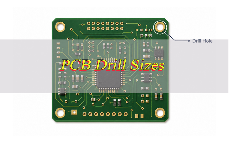
What Are PCB Drill Sizes?
PCB drill sizes are the hole diameters used to create vias, through holes, mounting holes, tooling holes and mechanical openings on a PCB. These holes can be produced by mechanical drilling or laser drilling, depending on the required diameter, depth and PCB structure.
In production, the drill size is only the starting value. After drilling, the PCB may go through desmear, copper plating, surface finish and final inspection. These steps can change the usable hole diameter, especially for plated holes.
A correct drill size must be selected together with finished hole size, pad diameter, annular ring, plating thickness, board thickness, drill tolerance and hole type. If these factors are not matched, the PCB may have poor insertion, soldering defects, weak vias or low production yield.
What Is the Difference Between Drill Size and Finished Hole Size?
Drill size is the original hole made by the drill bit, while finished hole size is the final hole diameter after plating and fabrication. This difference is most important for plated through holes because copper plating reduces the internal hole diameter.
For example, if a PCB design requires a 0.80 mm finished PTH hole, the actual drill size before plating may be larger. This extra allowance gives space for copper to be deposited on the hole wall while keeping the final opening suitable for the component lead.
For NPTH holes, the final size is usually closer to the mechanical drill diameter because the hole wall is not plated. PCB drawings should clearly state whether each value refers to drill size or finished hole size. This prevents CAM review errors, incorrect tool selection and assembly fit problems.
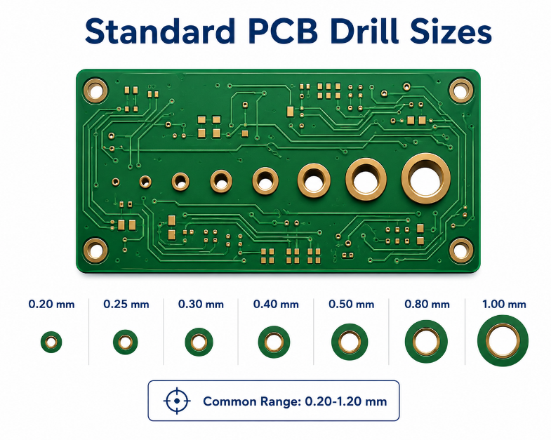
What Are Standard PCB Drill Sizes?
Standard PCB drill sizes usually range from 0.20 mm to 1.20 mm or larger for common mechanical drilling. Smaller HDI or advanced small vias may use tighter drilling processes or laser drilling, while larger holes are used for connectors, terminals, mounting screws, tooling holes and mechanical positioning.
| mm | mil | inch | Use |
|---|---|---|---|
| 0.15 | 6 | 0.0059 | HDI / advanced small via |
| 0.20 | 8 | 0.0079 | Small via |
| 0.25 | 10 | 0.0098 | Fine-pitch via |
| 0.30 | 12 | 0.0118 | Standard via |
| 0.40 | 16 | 0.0157 | Signal via |
| 0.50 | 20 | 0.0197 | Large via |
| 0.60 | 24 | 0.0236 | Small lead |
| 0.80 | 31 | 0.0315 | Resistor lead |
| 1.00 | 39 | 0.0394 | Connector pin |
| 1.20 | 47 | 0.0472 | Terminal hole |
The standard PCB drill sizes chart should be treated as a common design reference, not a universal rule for every PCB factory. Final selection still depends on finished hole size, plating allowance, tolerance, PCB thickness, aspect ratio and the manufacturer’s proven production capability.
How Do You Read a PCB Drill Size Chart?
A PCB drill size chart helps convert hole sizes between mm, mil and inch, and it helps compare drill size with finished hole requirements. This is useful when component datasheets, CAD libraries and fabrication notes use different units.
| mm | mil | inch |
|---|---|---|
| 0.20 | 7.87 | 0.0079 |
| 0.25 | 9.84 | 0.0098 |
| 0.30 | 11.81 | 0.0118 |
| 0.40 | 15.75 | 0.0157 |
| 0.50 | 19.69 | 0.0197 |
| 0.60 | 23.62 | 0.0236 |
| 0.80 | 31.50 | 0.0315 |
| 1.00 | 39.37 | 0.0394 |
| 1.20 | 47.24 | 0.0472 |
The key conversion is 1 inch = 25.4 mm, 1 mil = 0.001 inch, and 1 mm = 39.37 mil. A PCB drill bit size chart mm to inches prevents unit mistakes, while PCB drill size mm vs mil conversion helps engineers review Gerber files, datasheets and fabrication drawings more accurately.
What Size Drill Is Used for PCB Through Holes?
The drill size for PCB through holes depends on component lead diameter, insertion clearance, plating allowance and manufacturing tolerance. A through-hole component hole should not equal the lead diameter because the component must insert smoothly before soldering.
| Lead Dia. | Finished Hole | Typical Production Drill |
|---|---|---|
| 0.40 mm | 0.55–0.60 mm | 0.65–0.70 mm |
| 0.50 mm | 0.65–0.70 mm | 0.75–0.80 mm |
| 0.60 mm | 0.75–0.80 mm | 0.85–0.90 mm |
| 0.80 mm | 0.95–1.00 mm | 1.05–1.10 mm |
| 1.00 mm | 1.15–1.20 mm | 1.25–1.30 mm |
For most through-hole component drill sizes, the finished hole is commonly 0.15–0.25 mm larger than the maximum lead diameter. For engineers asking what size drill for PCB in mm, the safest method is to start from the datasheet lead diameter, add insertion clearance, then confirm the final production drill with the PCB manufacturer.
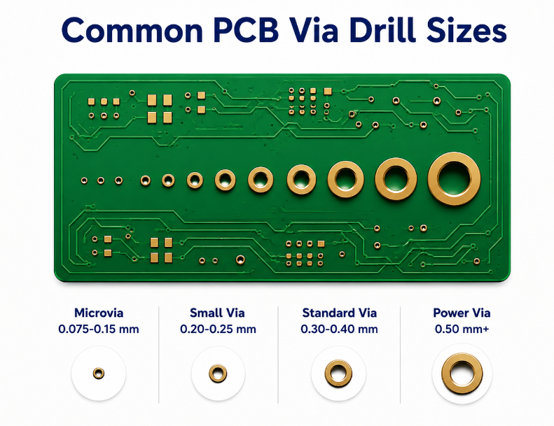
What Are Common PCB Via Drill Sizes?
Common PCB via drill sizes usually range from 0.20 mm to 0.50 mm for mechanical vias. The selected size depends on routing density, current requirement, thermal design, PCB thickness, layer count and plating capability.
| Via Type | Drill Size | Typical Pad Size | Use |
|---|---|---|---|
| Microvia | 0.075–0.15 mm | 0.20–0.35 mm | HDI routing |
| Small via | 0.20–0.25 mm | 0.45–0.55 mm | Dense layout |
| Standard via | 0.30–0.40 mm | 0.60–0.80 mm | Signal routing |
| Power via | 0.50 mm+ | 0.90 mm+ | Current path |
| Thermal via | 0.30–0.50 mm | 0.60–1.00 mm | Heat transfer |
Small vias save routing space and support fine-pitch fanout. However, smaller vias increase drilling difficulty, plating risk, inspection demand and cost, especially in thick multilayer PCB boards. For power or thermal use, larger vias may be more reliable than many undersized vias because they provide stronger copper plating and lower resistance.
What Is the Minimum PCB Drill Size?
The minimum PCB drill size depends on drilling method, PCB thickness, aspect ratio, plating requirement and process capability. In standard mechanical drilling, a practical minimum is often around 0.20–0.30 mm for many PCB projects.
For HDI PCB designs, laser-drilled microvias can be smaller, commonly around 0.075–0.15 mm, depending on stack-up and dielectric thickness. The minimum drill size for PCB via / HDI microvia should be confirmed before layout because it affects lamination, plating, reliability and cost.
Blind buried microvia drill size standard should be reviewed as part of the HDI stack-up, not as a standalone hole diameter. The smallest possible hole is not always the best option; stable mass production depends on proven capability, reliable plating and proper aspect ratio control.
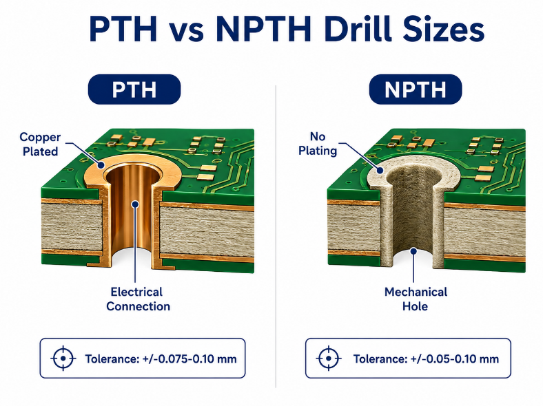
What Is the Difference Between PTH and NPTH Drill Sizes?
PTH drill sizes must allow for copper plating, while NPTH drill sizes are mainly controlled by mechanical drilling accuracy. PTH holes are used for electrical connection, and NPTH holes are used for mechanical location, screws, tooling or insulation clearance.
| Item | PTH | NPTH |
|---|---|---|
| Full Name | Plated Through Hole | Non-Plated Through Hole |
| Hole Wall | Copper plated | No copper plating |
| Final Size | Smaller after plating | Close to drilled size |
| Use | Vias, leads, electrical holes | Mounting, tooling, locating |
| Design Focus | Conductivity and solderability | Mechanical fit |
| Tolerance Factor | Drilling plus plating | Drilling accuracy |
PTH vs NPTH drill sizes tolerance should be separated in the fabrication drawing. Mixing plated and non-plated holes in one unclear drill table can cause wrong hole processing, poor fit or assembly problems. For mounting holes, NPTH design often gives better mechanical control because no copper plating changes the final diameter.
What Is the PCB Drill Hole Tolerance Standard?
PCB drill hole tolerance is the allowed size variation between the specified finished hole and the actual manufactured hole. It is affected by drilling accuracy, plating thickness, hole size, board thickness, material movement and inspection requirements.
The following values are common manufacturing tolerance ranges, not universal IPC limits. Final tolerance should be confirmed according to PCB class, hole type, size, thickness and supplier capability.
| Hole Type | Common Tolerance | Control Point |
|---|---|---|
| PTH small hole | ±0.075–0.10 mm | Finished hole |
| NPTH hole | ±0.05–0.10 mm | Mechanical fit |
| Mounting hole | ±0.10 mm+ | Diameter and position |
| Tight hole | ±0.05 mm | Extra inspection |
For normal PCB production, PTH finished hole tolerance is often around ±0.075–0.10 mm, while tighter holes may increase cost. IPC drill size guidelines focus less on one universal drill table and more on finished hole quality, annular ring, plating integrity, hole wall reliability and acceptance class. For critical holes, finished hole inspection, annular ring review, hole wall plating check and cross-section inspection are common quality controls.
How Do Aspect Ratio Limits Affect PCB Drill Sizes?
Aspect ratio decides whether a drilled hole can be plated reliably through the PCB thickness. The basic formula is PCB thickness divided by finished hole diameter. A small hole in a thick board creates a high aspect ratio and makes copper plating more difficult.
| Thickness | Hole Dia. | Aspect Ratio |
|---|---|---|
| 1.60 mm | 0.40 mm | 4:1 |
| 1.60 mm | 0.25 mm | 6.4:1 |
| 2.00 mm | 0.25 mm | 8:1 |
| 3.20 mm | 0.30 mm | 10.7:1 |
Many standard PCB designs stay within practical aspect ratio limits such as 6:1, 8:1 or 10:1, depending on factory capability. Higher aspect ratio holes increase plating risk, especially in thick multilayer PCB boards. When the board is thicker than 2.0 mm, small vias should be reviewed carefully before mass production.
What Is the Difference Between Mechanical Drill and Laser Drill?
Mechanical drilling is used for standard through holes, vias, NPTH holes and mounting holes, while laser drilling is used for small HDI microvias and blind vias. The process is selected according to hole size, depth, stack-up and routing density.
| Item | Mechanical Drill | Laser Drill |
|---|---|---|
| Size Range | 0.20 mm+ common; 0.15 mm possible in advanced process | 0.075–0.20 mm common |
| Hole Type | Through hole, via, NPTH | Blind microvia |
| Cost | Lower | Higher |
| Best Use | Standard PCB drilling | HDI breakout |
| Limit | Tool wear, drill wander | Depth control |
Mechanical drilling is more economical for common PCB drill sizes and high-volume standard holes. Laser drilling is better for fine-pitch BGA breakout, compact HDI routing and blind microvia structures. Using laser drilling only where necessary helps control PCB cost without sacrificing routing density.
How Do Non-Standard Drill Sizes Affect PCB Cost?
Non-standard drill sizes can increase PCB cost because they add tool changes, setup work, slower drilling, higher inspection demand and greater tool breakage risk. The cost impact becomes stronger when the PCB has many holes or very small diameters.
Key cost factors include:
- Extra drill tool changes, which increase machine time.
- Uncommon drill bits, which may require special preparation.
- Very small holes, which increase tool wear and breakage risk.
- Tight tolerance holes, which require additional measurement.
- High hole count, which extends drilling cycle time.
- High aspect ratio holes, which increase plating difficulty.
- Special inspection requirements, which add quality control time.
For cost-sensitive PCB projects, use standard PCB drill sizes whenever possible and avoid unnecessary custom hole diameters. During quotation, provide hole count, finished hole size, PTH/NPTH separation, tolerance and board thickness so the PCB manufacturer can price the drilling process accurately.
How Should You Choose the Right PCB Drill Size?
Choose the right PCB drill size by starting with the finished hole requirement, then checking plating allowance, tolerance, component lead diameter, aspect ratio and supplier capability. This prevents design problems before fabrication.
- Confirm the hole function. Vias, resistor holes, connector holes, mounting holes and tooling holes require different rules.
- Define the finished hole size. PTH holes require plating allowance; NPTH holes focus on mechanical fit.
- Check the component datasheet. Use the maximum lead diameter, not only the typical value.
- Protect the annular ring. Pad size must leave enough copper around the drilled hole.
- Review aspect ratio. Small holes in thick PCB boards are harder to plate reliably.
- Check inspection needs. Critical holes may require finished hole measurement, cross-section review or plating verification.
- Use standard drill sizes. Standard options reduce cost and improve production stability.
- Prepare quotation data. Send board thickness, hole count, smallest drill size, PTH/NPTH list, tolerance and HDI structure if applicable.
- Confirm special requirements early. HDI microvias, blind vias, buried vias, press-fit holes and tight tolerance holes should be reviewed before file release.
FAQs About PCB Drill Sizes
Q1: Can one PCB design use several different PCB drill sizes?
A1: Yes. One PCB can use different holes for vias, connector pins, resistor leads, mounting holes, tooling holes and test access. However, too many drill diameters increase drill tool changes and manufacturing time. A compact drill table with standard PCB drill sizes helps reduce cost, improve production consistency and simplify CAM review.
Q2: Is the drill size in a CAD library always correct for production?
A2: Not always. A CAD footprint may use a generic hole size, but real production must consider the component datasheet, plating allowance, insertion clearance and PCB supplier tolerance. Before mass production, the finished hole size should be checked against the actual component lead diameter and assembly method.
Q3: Should mounting holes be PTH or NPTH?
A3: Mounting holes are often NPTH when they are used only for screws, spacers or mechanical alignment. PTH mounting holes may be selected when grounding, shielding or chassis connection is required. The choice depends on mechanical fit, electrical function, clearance requirement and whether the screw area should connect to copper.
Q4: What should be included in a PCB drill file?
A4: A complete drill file should include hole coordinates, drill diameters, units, plated hole data, non-plated hole data and slot information if applicable. The fabrication drawing should also define finished hole size, tolerance and special holes. Clear drill data reduces CAM questions and prevents wrong hole processing.
Q5: Why do Gerber files and drill files sometimes show different hole information?
A5: Gerber files describe copper, solder mask and silkscreen layers, while Excellon drill files define drilled hole positions and sizes. If the CAD export is incomplete, the drill table may not match the layout. Before ordering PCB fabrication, check that Gerber, drill file and fabrication drawing use the same units and hole definitions.
Q6: What is drill wander in PCB manufacturing?
A6: Drill wander means the drill shifts slightly away from the intended center point during drilling. It can reduce annular ring width, cause breakout or create reliability risk in small pads. Proper annular ring allowance, manufacturable pad size and stable drill diameters help reduce the effect of drill wander.
Q7: How does annular ring affect PCB drill size selection?
A7: Annular ring is the copper area between the drilled hole edge and the pad edge. If the drill is too large or the pad is too small, the remaining copper ring may be weak. Drill size and pad size must be selected together to maintain electrical reliability and pass inspection.
Q8: Do PCB drill sizes affect solder mask design?
A8: Yes. Large holes, dense vias and exposed test points may require proper solder mask openings or tenting rules. For vias near fine-pitch components, mask design affects solder bridging and contamination risk. Drill size, pad size and solder mask clearance should be reviewed together during PCB layout.
Q9: Can vias be plugged, tented or filled after drilling?
A9: Yes. Vias can be tented with solder mask, plugged with resin or filled and capped for HDI and BGA designs. The choice depends on assembly process, via location and reliability target. Via filling requirements should be stated clearly because they affect cost, lead time and surface flatness.
Q10: Do PCB drill sizes affect high-speed signal quality?
A10: Yes. Via drill diameter, pad size, anti-pad size and via stub length can affect impedance and signal integrity in high-speed PCB designs. For fast signals, uncontrolled vias may create reflection or loss. Controlled impedance boards should review via structure together with stack-up and return path.
Q11: How does copper thickness affect PCB drilling?
A11: Heavy copper PCB may require larger pads, stronger annular ring control and careful hole wall plating. Thick copper also increases manufacturing difficulty around small holes and dense vias. For heavy copper boards, drill size, copper weight, spacing and plating capability should be reviewed before production.
Q12: What is the best way to reduce PCB drilling cost?
A12: The best approach is to use common drill diameters, reduce unnecessary hole count, avoid overly tight hole tolerance and confirm minimum drill capability early. Non-standard sizes and very small holes increase machining and inspection time. A clean drill table helps the PCB factory quote faster and manufacture more efficiently.
Q13: Are blind vias and buried vias more expensive than through vias?
A13: Yes. Blind and buried vias usually increase cost because they require additional drilling, lamination and inspection steps. HDI microvias may also require laser drilling and via filling. They should be used where routing density or BGA breakout requires them, not as a default replacement for standard through vias.
Q14: What inspection methods are used for PCB drilled holes?
A14: Common inspection methods include finished hole measurement, annular ring check, visual inspection, electrical continuity testing and cross-section inspection for critical PTH holes. For high-reliability PCB, hole wall plating quality is especially important. Inspection confirms that the drilled hole meets size, plating and reliability requirements.
Q15: What information should buyers send for a PCB drill size review?
A15: Buyers should send Gerber files, Excellon drill files, fabrication drawings, board thickness, stack-up, PTH/NPTH separation, finished hole tolerance, smallest drill size and special via requirements. For HDI, press-fit connectors or thick multilayer PCB, complete drill information helps prevent delays and improves quotation accuracy.
Choosing proper PCB drill sizes directly affects PCB manufacturability, assembly quality and long-term reliability. A reliable design should confirm finished hole size, PTH or NPTH type, annular ring, tolerance, aspect ratio, via structure and inspection requirements before releasing files for production.
If your PCB project includes HDI microvias, thick multilayer boards, press-fit connectors, tight tolerance holes, heavy copper or custom drilling requirements, our China PCB factory can review your Gerber files and drill table before production. Send your PCB files, board thickness, stack-up, PTH/NPTH list and tolerance notes to EBest Circuit via sales@bestpcbs.com. We can help you optimize drill sizes, reduce manufacturing risk and provide a fast PCB quotation for prototype or batch production.
You may also like


Tags: common pcb drill sizes, minimum pcb drill size, pcb drill size chart, pcb drill sizes mm, standard pcb drill sizes