PCB manufacturing PCB manufacturing
Home > Blog

Rogers RO4450F Prepreg: Multilayer PCB Stackup Guide

August 21st, 2026

Rogers RO4450F prepreg is a high-frequency thermoset bonding material, also known as bondply, used to bond dielectric cores, copper layers, and copper foil in multilayer RF and microwave PCBs. It is generally considered when a design uses RO4000-series laminates and requires predictable dielectric spacing, reliable resin filling, controlled impedance, or sequential lamination. It is not a copper-clad core and is usually unnecessary for a simple two-layer board built from a single Rogers core.

EBest Circuit supports Rogers and Rogers/FR-4 hybrid PCB fabrication, including stackup review, controlled impedance, prototypes, and volume production. For an engineering review, send the Gerber files, proposed stackup, Rogers material grade, dielectric thickness, copper weight, target impedance, operating frequency, and quantity to sales@bestpcbs.com.

This guide covers RO4450F thickness, RO4450F Dk, compatible Rogers materials, lamination controls, and the information needed to quote a multilayer RF PCB.

Rogers RO4450F prepreg for multilayer RF and microwave PCB stackups

What Is Rogers RO4450F Prepreg?

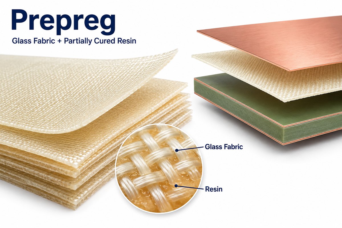
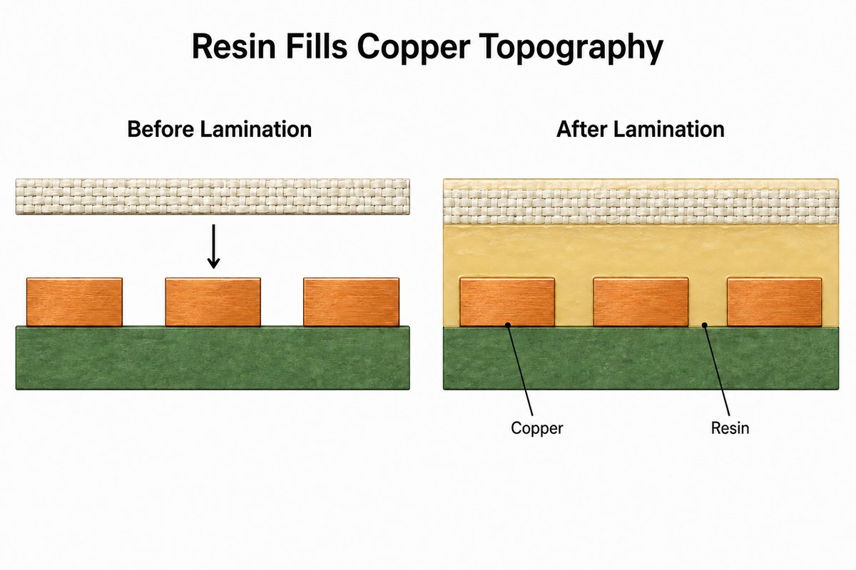
Rogers RO4450F is a glass-reinforced, hydrocarbon-ceramic thermoset bonding material in the RO4400 family. Before lamination, it is supplied as an uncured sheet without copper. During pressing, its resin softens, flows around etched copper features, and then cures to join the PCB layers.

After curing, RO4450F performs two functions:

  • It provides mechanical bonding between the layers.
  • It becomes part of the electrical dielectric structure.

This second function is especially important in stripline and other controlled-impedance structures. The bondply’s dielectric constant and final pressed thickness influence the distance between a signal trace and its reference plane.

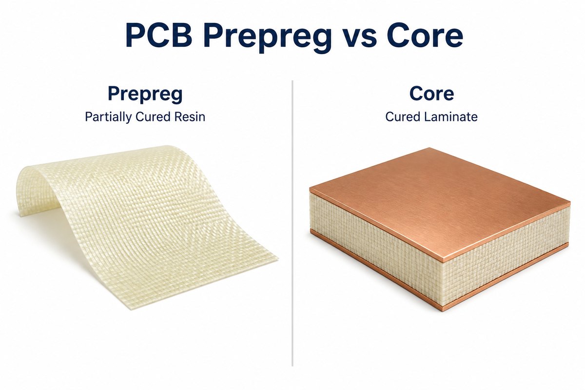
RO4450F should not be described as a complete “RO4450F PCB laminate.” A laminate or core normally contains a cured dielectric with copper on one or both sides. RO4450F is the bonding layer placed between cores, inner layers, or copper foil.

It is appropriate for multilayer RF boards that need RO4000-compatible bonding. A two-layer RO4350B or RO4003C PCB made from one copper-clad core normally does not require bondply because no additional layers need to be laminated.

What Are the Key RO4450F Datasheet Values?

The following values come from the Rogers RO4450F and RO4460G2 bondply datasheet. They are typical material values rather than guaranteed finished-PCB results. Design teams should check the test method and obtain current material documentation before releasing a production stackup.

Property RO4450F typical value Design relevance
Material type High-frequency thermoset bondply Used between layers, not as a copper-clad core
Standard thickness 0.0040 in / 0.102 mm Starting point for stackup planning
Thickness tolerance ±0.0006 in Must be considered in dielectric-height analysis
Dielectric constant 3.52 ± 0.05 at 10 GHz Influences impedance and signal velocity
Dissipation factor 0.004 at 10 GHz Contributes to transmission loss
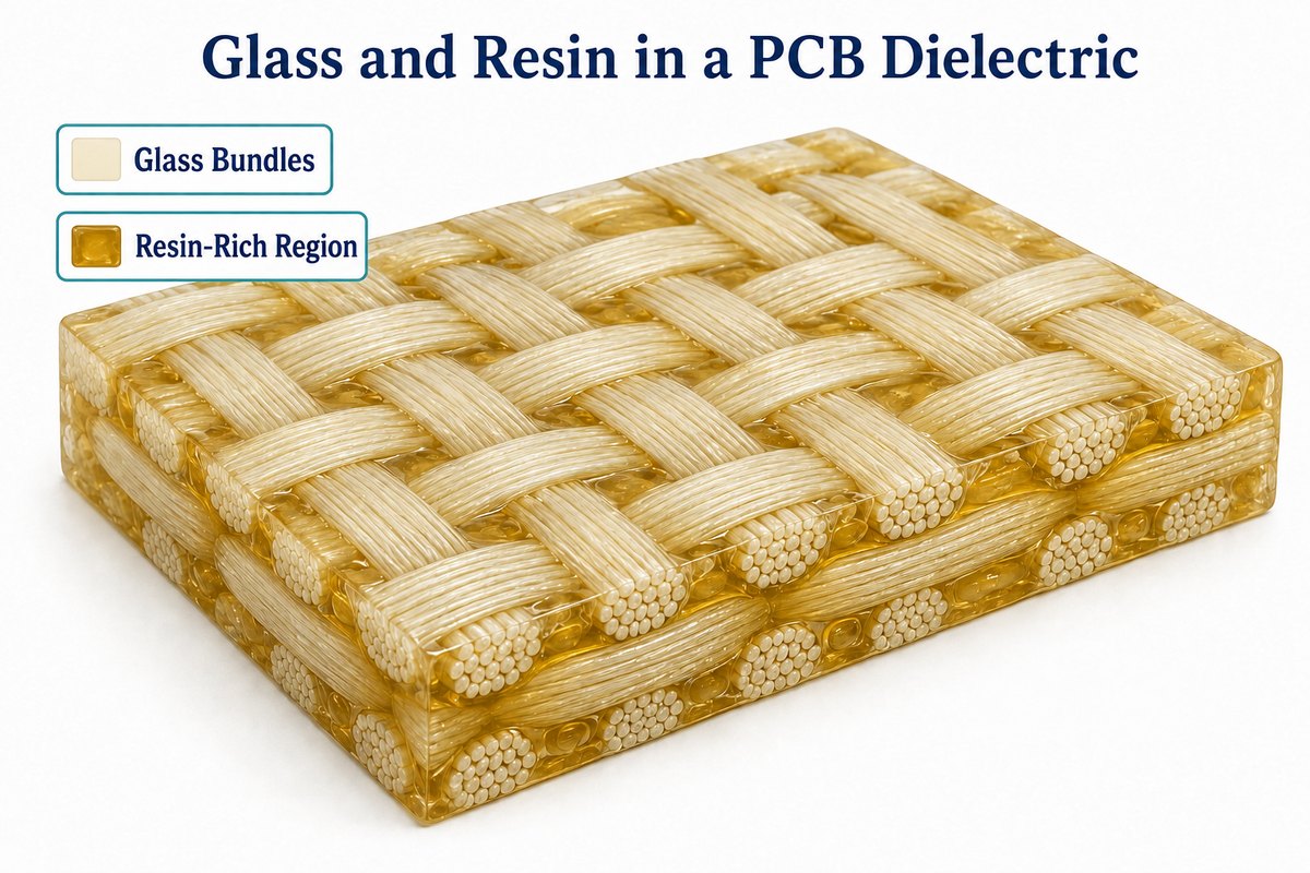
Glass style 1080 Influences resin distribution and local dielectric behavior
Resin content 80% Supports filling around etched copper
Glass transition temperature Above 280°C Supports multiple lamination cycles after full cure
Decomposition temperature 390°C Indicates thermal decomposition resistance
Thermal conductivity 0.65 W/m·K Relevant to thermal modeling, but not a heat-spreading solution
CTE, X/Y/Z 19/17/50 ppm/°C Relevant to dimensional and plated-hole reliability
Moisture absorption 0.04% under D24/23 conditions Test conditions must be retained when comparing data
Flammability UL 94 V-0 Suitable for applications requiring this material rating
Lead-free compatibility Yes Compatible with lead-free assembly processes

The Dk value of 3.52 should not be entered into every field solver without context. Rogers reports it using a defined IPC test method on raw material. Actual circuit behavior also depends on cured thickness, glass weave, copper roughness, trace geometry, frequency, and the measurement model used by the PCB manufacturer.

The official values and test conditions are available in the Rogers RO4450F bondply datasheet.

How Does RO4450F Work in a Multilayer PCB Stackup?

RO4450F is positioned between etched cores, inner-layer copper surfaces, or copper foil before the multilayer book is pressed. As the temperature rises, the resin reaches a low-viscosity range and flows into spaces around the copper pattern. Continued heat and pressure cure the resin and form a stable dielectric layer.

A typical multilayer construction may contain:

  • An RO4350B or RO4003C RF core
  • An etched inner copper layer
  • One or more plies of RO4450F
  • A reference plane or copper foil
  • Additional Rogers or FR-4 layers

The bondply quantity cannot be determined from layer count alone. The manufacturer must examine copper thickness, retained copper percentage, open areas, opposing plane layers, venting features, and the required final dielectric spacing.

RO4450F is most valuable when its improved lateral flow helps fill a challenging copper pattern. However, adding more plies simply to improve filling also increases dielectric thickness. That can change impedance and may require different trace widths, so resin fill and electrical geometry must be reviewed together.

RO4450F multilayer PCB stackup during fabrication layup

Which Rogers Laminates Are Compatible with RO4450F?

Rogers identifies RO4450F as compatible with multilayer constructions using RO4000-series materials, including RO4003C, RO4350B, RO4835, RO4360G2, and RO4000 LoPro laminates.

The most common pairings include:

  • RO4003C: Often selected for commercial RF and microwave boards where performance and material cost must be balanced.
  • RO4350B: Suitable for high-frequency multilayer designs that also require a UL 94 V-0-rated core material.
  • RO4835 and RO4360G2: Used when their specific electrical, thermal, or environmental properties match the application.
  • RO4000 LoPro: Useful when smoother copper is required to reduce conductor loss at higher frequencies.

Material compatibility does not mean that different cores can be exchanged without modifying the design. Each grade has its own Dk, Df, available thicknesses, copper options, thermal behavior, and processing requirements. Replacing RO4350B with RO4003C, for example, can change impedance and loss even if both can be bonded with RO4450F.

The exact core grade, copper foil type, dielectric thickness, and RO4450F ply count should therefore appear in the controlled stackup rather than being left to the manufacturer after quotation.

What Determines the Pressed Thickness of RO4450F?

Each RO4450F ply bonds to approximately 0.004 inch, or 0.101 mm, when pressed between opposing flat surfaces. In an actual PCB, the thickness contributed by that ply changes because some resin moves into the spaces between copper features.

The main factors are:

  • Inner-layer copper weight
  • Percentage of copper remaining after etching
  • Distribution of copper across the panel
  • Plane-to-plane or signal-to-plane construction
  • Number of RO4450F plies
  • Lamination pressure and thermal profile
  • Venting and flow patterns outside the functional circuit area

According to Rogers’ processing guidance, RO4450F can fill up to 0.0018 inch of total copper thickness under the stated design conditions. Additional bondply may be required when the filling requirement exceeds approximately 0.002 inch. This is particularly relevant to heavy inner copper and layers with large differences between dense and open copper areas.

A designer should not set controlled impedance from the nominal 4 mil value alone. The PCB manufacturer should calculate or estimate the finished dielectric thickness from the real copper pattern and validated press process. The resulting production stackup can then be returned to the designer for approval before fabrication.

How Does RO4450F Affect Controlled Impedance?

RO4450F affects controlled impedance whenever it forms part of the dielectric path between a signal trace and a reference plane. Both its Dk and its cured thickness influence the impedance result.

For an internal stripline, a thinner-than-expected RO4450F layer moves the trace closer to the reference plane and generally lowers impedance. A thicker layer generally raises impedance when the remaining geometry is unchanged. Trace width, copper thickness, trapezoidal etching, and copper roughness create additional variation.

The impedance review should include:

  • Target single-ended or differential impedance
  • Operating frequency or signal rise time
  • Trace width and spacing
  • Finished copper thickness
  • Dielectric height above and below the trace
  • Dk value and calculation method
  • Copper foil type and roughness
  • Manufacturing tolerance
  • Coupon and test requirements

For RF transmission lines, insertion loss and phase behavior may be just as important as nominal impedance. A prototype should therefore be verified electrically when the stackup is new, the frequency is high, or the acceptable tolerance is narrow.

The drawing should identify the required impedance but allow the fabricator to make controlled trace adjustments after calculating the approved production stackup. Locking the trace geometry while leaving the final material construction undefined creates avoidable quotation delays and engineering questions.

Controlled impedance and pressed dielectric thickness measurement

Can RO4450F Be Used in Rogers and FR-4 Hybrid Stackups?

RO4450F can be used in selected Rogers/FR-4 hybrid multilayer constructions. Rogers states that RO4400 bondply uses FR-4-compatible bonding temperatures and can be combined with low-flow FR-4 bondply in a non-homogeneous stackup using one bonding cycle.

Hybrid construction can reduce material cost by placing Rogers laminates only where RF or high-speed performance requires them. Power, control, or low-speed routing layers may remain on FR-4 if their electrical and thermal requirements permit it.

However, the stackup must account for differences in:

  • Dielectric constant and dissipation factor
  • Z-axis and in-plane expansion
  • Resin flow
  • Copper adhesion treatment
  • Glass transition behavior
  • Moisture response
  • Finished thickness and warpage
  • Drilling and desmear requirements

Standard FR-4 prepreg should not automatically replace RO4450F next to an impedance-controlled RF trace. Its dielectric properties and loss may be unsuitable for that transmission-line structure. A hybrid approach works best when the electrical role of every dielectric layer is clearly defined.

Hybrid construction is unnecessary when every layer carries performance-sensitive RF signals or when the savings from replacing a small amount of Rogers material do not justify the additional stackup and process complexity.

Rogers and FR-4 hybrid PCB stackup with RO4450F prepreg

How Does RO4450F Compare with RO4450B and RO4450T?

The correct choice depends primarily on approved legacy construction, resin-filling requirements, and the dielectric thickness options needed by the stackup.

Selection point RO4450F RO4450B RO4450T
Current design role RO4000-compatible bondply with improved lateral flow Referenced in earlier RO4400 documentation and existing designs Spread-glass bondply with more thickness choices
Nominal thickness options Primarily 0.004 in Depends on the applicable legacy specification Approximately 0.0025 to 0.006 in, depending on grade
Dk 3.52 ± 0.05 at 10 GHz Must be confirmed from the approved specification Varies with thickness; not one universal value
Main advantage Better filling for demanding copper patterns May already be qualified in a legacy product Greater dielectric-thickness flexibility
Best-fit decision New designs or difficult fill conditions Existing validated stackups High-layer-count designs needing more thickness choices
Substitution approach Review Dk, thickness, fill, and impedance Do not replace based only on the family name Recalculate the stackup for the selected thickness

RO4450F should not replace RO4450B solely because it has better lateral flow. A substitution can change dielectric thickness, Dk, resin volume, impedance, and an already qualified thermal history. For an established product, review the material declaration, approved vendor list, validation records, and change-control requirements first.

RO4450T is more appropriate when the design needs finer control over dielectric spacing. RO4450F remains attractive when a 4 mil bondply fits the electrical geometry and copper filling is the stronger concern.

What Should Fabricators Check During RO4450F Lamination?

RO4450F lamination requires controlled storage, clean handling, suitable inner-layer preparation, and a press profile matched to the actual copper pattern.

Rogers’ processing guide identifies several important controls:

  • Store the bondply at 10°C to 32°C and protect it from ultraviolet light.
  • Keep unused material in sealed packaging and follow first-in, first-out control.
  • Do not store it frozen, refrigerated, or under vacuum.
  • Keep slip sheets in place during handling and tooling to limit contamination.
  • Treat inner-layer copper with an appropriate oxide or oxide-alternative process.
  • Bake prepared inner layers for 15–20 minutes at 115°C to 125°C before layup.
  • Provide sufficient time in the 100°C to 120°C low-viscosity range for resin filling.
  • Use vacuum assistance where available and verify the thermal profile with thermocouples.
  • Maintain traceability for material lots, press cycles, and stackup records.

The published guide describes bonding pressures in the 400–750 psi range and a 175°C curing stage, but these numbers should not be copied into an uncontrolled press recipe. Board thickness, layer count, copper distribution, press equipment, book loading, and lagging materials influence the process window.

Special review is advisable for designs with more than six metal layers, copper of 35 µm or thicker, opposing plane layers, single bondply plies over demanding copper patterns, or bonding to FR-4 cores. The complete Rogers RO4400 processing guide should be used alongside the fabricator’s validated process.

RO4450F prepreg lamination preparation in a PCB factory

What Causes Voids, Delamination, or Impedance Deviation in RO4450F Boards?

Most RO4450F defects originate from a mismatch between the copper structure, available resin, surface condition, and lamination process.

Problem Likely cause Practical prevention
Resin voids Insufficient resin, poor venting, contamination, or inadequate time in the flow window Review copper topography, venting, ply count, cleanliness, and press profile
Delamination Weak copper preparation, moisture, contamination, or incomplete cure Control storage, inner-layer treatment, pre-bake, pressure, and curing records
Local thickness variation Unbalanced copper or large open areas Improve copper balance and calculate pressed thickness by layer
Impedance deviation Incorrect Dk, dielectric height, trace width, or copper-thickness assumptions Approve the production stackup and use impedance coupons
Registration error Thin inner layers, unsuitable tooling, or excessive material movement Match tooling and pinning strategy to the required registration tolerance
PTH reliability problems Excessive thermal stress, unsuitable hole-wall preparation, or material mismatch Inspect drilled holes and use a compatible desmear process
Surface discoloration or hardened sheets Open-package exposure or poor inventory control Reseal partial packs and discard visibly affected material

Traditional chemical desmear should also be reviewed carefully. Rogers notes that CF4/O2 plasma is preferred when desmear is necessary, while etchback of the core and prepreg layers is not recommended.

Failure prevention is cheaper at stackup approval than after fabrication. A cross-section, impedance report, material certificate, electrical test, and controlled process record provide more useful evidence than relying only on the material name printed on the purchase order.

Which PCB Applications Use RO4450F?

RO4450F is best suited to multilayer boards in which Rogers RO4000-series cores require a compatible bonding layer and the cured bondply affects electrical or mechanical performance.

Common applications include:

  • Backhaul radio equipment
  • RF power amplifiers
  • Small cells and distributed antenna systems
  • Microwave communication modules
  • RF filters and signal-distribution boards
  • Antenna feed networks
  • Test and measurement equipment
  • High-speed communication hardware
  • Mixed-material RF and digital multilayer PCBs

It is particularly useful when an RF design needs buried routing, internal reference planes, transitions between RF and digital sections, or multiple lamination cycles.

RO4450F may be unnecessary for a two-layer RF board, a low-frequency industrial controller, or a cost-sensitive design whose dielectric loss and impedance stability can be met with a suitable FR-4 system. Selecting it without a clear electrical or structural reason adds material cost and supply-chain constraints without creating a corresponding performance benefit.

RF and microwave PCB testing with a vector network analyzer

What Information Is Needed for an RO4450F PCB Quote?

A reliable quotation requires more than the Gerber files and board dimensions. The manufacturer must understand the intended electrical geometry and which parts of the material specification are fixed.

Provide the following information:

  • Gerber or ODB++ fabrication data
  • Layer count and proposed stackup
  • Exact Rogers core grades
  • RO4450F ply location and quantity, if already defined
  • Core and dielectric thicknesses
  • Finished board thickness and tolerance
  • Base and finished copper weights
  • Controlled-impedance targets and tolerances
  • Operating frequency or critical signal requirements
  • Via types, finished hole sizes, and aspect ratios
  • Surface finish
  • Solder mask requirements
  • Panel or individual board dimensions
  • Prototype and production quantities
  • Required inspection reports or impedance data
  • Applicable acceptance class or customer specification

If the pressed dielectric height is not finalized, identify the electrical constraints rather than inserting an assumed value. The manufacturer can then propose a producible stackup for approval.

EBest Circuit can review Rogers and Rogers/FR-4 hybrid stackups before quotation. Sending the material grade, copper weight, target impedance, operating frequency, and proposed layer arrangement at the beginning reduces engineering questions and helps keep the prototype consistent with later production.

FAQs About Rogers RO4450F Prepreg

Is RO4450F a core or a prepreg?

RO4450F is a prepreg or bondply, not a copper-clad core. It is placed between PCB layers during lamination and becomes a cured dielectric after pressing.

Can RO4450F be laminated with RO4350B or RO4003C?

Yes. Rogers identifies RO4450F as compatible with RO4350B, RO4003C, and several other RO4000-series laminates. The complete stackup still needs review for thickness, impedance, copper filling, and lamination conditions.

What is the standard thickness of RO4450F?

The standard sheet thickness is 0.0040 inch, or approximately 0.102 mm, with a published tolerance of ±0.0006 inch. Its actual contribution to a PCB stackup depends on the copper thickness and distribution surrounding the bondply.

Can RO4450F be used with 1 oz or thicker inner copper?

It can be used with 1 oz copper, but the retained copper pattern and total filling requirement must be reviewed. Rogers recommends additional technical review for copper layers of 35 µm or thicker because a single ply may not provide enough resin for every pattern.

Can RO4450F replace RO4450B directly?

Not without engineering approval. Even materials from the same family can differ in thickness, Dk, availability, flow behavior, and qualification status, so the controlled stackup and impedance calculation must be checked.

Is RO4450F suitable for sequential lamination?

Yes. Its high post-cure Tg allows fully cured RO4400 bondply to withstand additional lamination cycles. The complete thermal history, via structure, and inner-layer preparation still need to match the fabricator’s validated process.

Can standard FR-4 prepreg replace RO4450F?

Standard FR-4 prepreg may be acceptable in non-critical layers, but it is not a direct electrical substitute near an RF transmission line. Differences in Dk, Df, thickness, and thermal behavior can change impedance, loss, and reliability.

RO4450F is a practical bonding material for multilayer RF PCBs when a design uses RO4000-series cores, requires controlled dielectric spacing, or presents demanding copper-fill conditions. Its nominal datasheet values are only the starting point; the final decision should be based on pressed thickness, copper distribution, impedance requirements, layer construction, and a controlled lamination process.

If you are planning a Rogers RO4450F multilayer PCB, send your Gerber files, stackup, material grades, copper weights, impedance targets, operating frequency, and quantity to EBest Circuit at sales@bestpcbs.com for engineering review and quotation.
You may also like

High Temperature PCB Material: How to Choose for Heat and Reliability

August 21st, 2026

A high temperature PCB material must do more than survive one hot assembly cycle. It needs to maintain insulation, dimensional stability, copper adhesion, and plated-hole reliability throughout the product’s real thermal profile. The correct choice depends on operating temperature, dwell time, cycling rate, heat flow, voltage, frequency, stackup, and expected service life.

At EBest Circuit, we manufacture high-Tg FR-4 and work with polyimide, high temperature ceramic substrate, and selected high-performance laminate systems for demanding PCB applications. We begin with the actual environment rather than selecting the highest Tg on a datasheet. This prevents both under-specification and unnecessary material cost. For an initial material review, you can send the stackup, operating and peak temperatures, Gerber files, copper requirements, quantity, and test conditions to sales@bestpcbs.com.

High Temperature PCB Material infographic showing high-Tg FR-4, polyimide and ceramic

What Is a High Temperature PCB Material?

A high-temperature material is a laminate or substrate that retains the required electrical and mechanical properties under a defined thermal load. That definition is intentionally application-specific. A board that sees three lead-free reflow cycles has a different exposure from an industrial controller operating near a furnace for years.

Engineers should separate three temperature cases:

  • Assembly peaks: short soldering and rework excursions.
  • Continuous operation: the steady temperature near the board or component.
  • Thermal cycling: repeated movement between low and high temperatures.

The weakest part of the finished structure may be the resin, copper interface, plated hole, solder joint, coating, connector, or component rather than the laminate itself. A reliable material specification therefore starts with the complete use profile, not a single headline temperature.

Which Properties Matter Beyond Tg?

Tg, or glass transition temperature, is the region where a resin changes from a rigid glassy state to a softer state with faster expansion. It helps classify resin systems, but it is not the board’s continuous-use rating.

The following properties provide a more complete picture:

Property What It Indicates Why It Matters
Tg Resin transition region Dimensional stability and expansion behavior
Td Onset of chemical decomposition under the stated test method Resistance to severe thermal exposure
T260/T288 Time to delamination at a specified temperature Assembly and rework robustness
Z-axis CTE Expansion through board thickness Stress on plated holes and vias
Thermal conductivity Rate of heat movement through material Junction temperature and heat spreading
Moisture absorption Water uptake under test conditions Reflow defects and insulation stability
Dk and Df Dielectric behavior and loss Impedance, timing, and RF/high-speed performance

Compare values only when the test method, material thickness, resin content, and conditioning are compatible. A higher Tg does not guarantee lower Z-axis expansion, better heat transfer, or lower signal loss.

High Temperature PCB Materials

The main high temperature pcb materials solve different problems. Some resist resin softening, some conduct heat efficiently, and others preserve electrical behavior at high frequency.

High Temperature PCB Materials comparison of high-Tg FR-4, polyimide and ceramic
Material Family Main Strength Main Limitation Typical Fit
High-Tg FR-4 Familiar multilayer processing and improved thermal stability Modest thermal conductivity Industrial controls, automotive electronics, multilayer boards
Polyimide High thermal endurance and flex compatibility Moisture and process control require attention Rigid-flex, aerospace, sensors, repeated thermal exposure
Ceramic High-temperature stability, insulation, and heat transfer Brittle and relatively costly Power modules, LEDs, sensors, harsh environments
High-frequency laminate Controlled Dk/Df and selected high-Tg options Higher material and fabrication cost RF, microwave, radar, high-speed links
Metal-core or thermal-spreading structure Moves heat toward a chassis or heatsink Limited routing freedom in common constructions Power conversion and high-power lighting

High-Tg FR-4 is usually the practical first candidate for a conventional rigid multilayer board. Polyimide becomes attractive when thermal endurance, flexibility, or repeated cycling dominates. Ceramic is justified when electrical isolation and heat transfer must be combined in a compact structure. RF materials should be chosen primarily from electrical loss and dielectric stability, then checked for thermal compatibility.

For a broader overview of laminate families, see our PCB material guide.

How Does High-Tg FR-4 Compare With Polyimide?

High-Tg FR-4 retains the established glass-fabric and epoxy-style production route used for many rigid multilayer PCBs. It offers a useful balance of cost, availability, drill behavior, lamination control, and lead-free assembly resistance. Our internal manufacturing source lists low-Tg FR-4 at 130–140°C, mid-Tg FR-4 at 150°C, and high-Tg FR-4 at 170–180°C; the exact laminate family still needs confirmation for each build.

Polyimide generally provides a higher thermal margin and is the standard foundation for flexible circuitry. It can also support rigid high-reliability constructions. However, resin chemistry, moisture handling, dimensional movement, bond system, and fabrication profile must all be controlled.

Choose between them using the application:

  • Use high-Tg FR-4 when a rigid board needs stronger reflow and thermal-cycling performance without moving to a specialized material system.
  • Consider polyimide when service temperature, repeated flexing, low outgassing requirements, or severe thermal cycling makes FR-4 unsuitable.
  • Do not substitute one for the other without checking stackup thickness, copper balance, drilling, lamination, and assembly requirements.

When Is a High Temperature Polyimide PCB the Better Choice?

A high temperature polyimide pcb is often the better choice when the circuit must flex, fit a three-dimensional enclosure, or tolerate repeated thermal exposure. Common examples include engine-area sensors, aerospace instruments, downhole equipment, heaters, and compact rigid-flex assemblies.

Polyimide selection still requires several decisions:

  • Adhesiveless or adhesive-based copper-clad laminate.
  • Static-flex or dynamic-flex construction.
  • Rolled-annealed or electrodeposited copper.
  • Coverlay, bondply, stiffener, and rigid-area material compatibility.
  • Moisture storage, baking, and assembly controls.

The bend area should not contain abrupt copper-width changes, unsupported vias, sharp corners, or an unsuitable grain direction. High thermal capability cannot compensate for a mechanically weak flex layout.

When Is a High Temperature Ceramic PCB Appropriate?

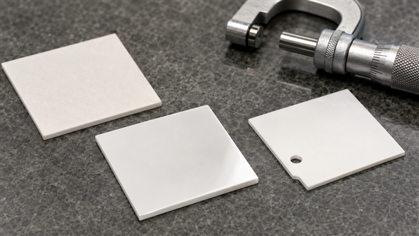
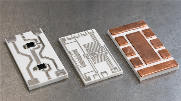
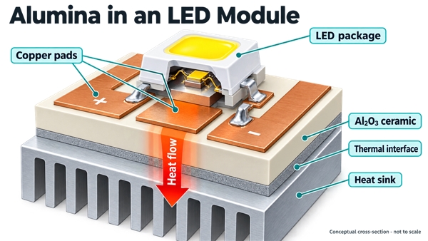
A high temperature ceramic pcb is appropriate when heat must move through an electrically insulating substrate while the circuit also needs low expansion and dimensional stability. Alumina and aluminum nitride are common choices, but their heat-transfer capability, strength, availability, metallization, and cost differ.

Ceramic is often considered for:

  • Power modules and high-current semiconductor assemblies.
  • High-power LEDs and laser drivers.
  • Automotive, industrial, and energy sensors.
  • RF modules requiring stable substrate properties.
  • Circuits exposed to high temperature or aggressive environments.

Ceramic is not simply a premium replacement for FR-4. It is brittle, panelization and machining differ, and copper attachment or metallization becomes part of the thermal-mechanical design. The ceramic grade, thickness, copper system, mounting method, and heatsink interface should be assessed together.

How Should High Temperature PCB Design Address Heat and Expansion?

Good high temperature pcb design controls both temperature and mechanical strain. Material selection is only one part of that work.

High Temperature PCB Design infographic showing a heat source, thermal path and Z-axis expansion

Use these design measures where the application requires them:

  • Place heat-generating components to create a short, predictable path to copper planes, thermal vias, a chassis, or a heatsink.
  • Use adequate copper area and balanced copper distribution to reduce local hot spots and warpage.
  • Keep high-expansion laminate regions from overstressing dense via fields.
  • Size plated holes and annular rings for the board thickness and thermal-cycle target.
  • Avoid resin-starved regions around heavy copper and tightly packed features.
  • Check component, solder alloy, connector, coating, and enclosure limits against the same temperature profile.
  • Model or measure board temperature at the hottest operating condition rather than relying only on ambient temperature.

The PCB board stackup should be finalized with the fabricator. Glass style, resin content, copper weight, dielectric thickness, and material pairing affect both thermal movement and manufacturability.

How Do Fabrication and Assembly Affect Thermal Reliability?

Fabrication exposes a multilayer board to lamination heat, drilling, desmear, copper plating, solder-mask cure, surface finishing, and assembly. A material can have strong datasheet values and still fail if the process window is not matched to its chemistry.

Important controls include:

  • Material storage and baking: Moisture can cause blistering, delamination, or conductive reliability problems during heating.
  • Lamination profile: Heat-up rate, pressure, vacuum, cure time, and cooling influence resin flow and registration.
  • Hole preparation: Drill parameters and desmear chemistry must create a clean surface for dependable copper plating.
  • Copper plating: Adequate and uniform barrel copper is essential because plated holes carry Z-axis strain.
  • Assembly profile: Peak temperature, time above liquidus, the number of reflow cycles, selective soldering, and rework all add thermal history.
  • Handling after assembly: Cleaning, coating, mounting torque, and heatsink attachment can introduce additional stress.

Material equivalence should be approved from a property set, not a Tg value alone. If an alternate laminate is proposed, compare its datasheet, processing behavior, impedance model, and qualification requirements.

What Causes High-Temperature PCB Failures?

Most thermal failures are interactions between material, geometry, process, and operating conditions.

Common modes include:

  • Barrel cracking: Z-axis expansion strains plated through holes during cycling.
  • Pad lifting or copper separation: Heat and mechanical force weaken the copper-to-resin interface.
  • Delamination or blistering: Moisture, insufficient cure, contamination, or excessive thermal exposure separates layers.
  • Warpage: Unbalanced copper, asymmetric stackups, large temperature gradients, or incompatible materials distort the board.
  • Insulation degradation: Heat, voltage, moisture, and contamination reduce electrical isolation.
  • Solder-joint fatigue: Different expansion rates between the PCB, package, and solder repeatedly strain the joint.
  • Local overheating: Poor heat spreading raises component and laminate temperature even when ambient conditions appear acceptable.

A useful stop condition is any operating point where the measured board temperature, deformation, insulation resistance, or interconnect performance leaves the validated range. At that point, the design needs a different material, improved cooling, a revised stackup, or a lower electrical/thermal load.

How Should Materials Be Tested and Qualified?

Qualification should reproduce the stresses that matter to the product. A generic thermal test is rarely enough.

High-Temperature PCB Qualification with thermal cycling, repeated reflow and microsection checks

A practical plan may include:

  • Incoming laminate certificate and lot traceability review.
  • Tg, Td, T260/T288, CTE, moisture, Dk/Df, or thermal-conductivity data as applicable.
  • Solder-float or repeated-reflow coupons for assembly exposure.
  • Thermal cycling or thermal shock using the product’s temperature range and dwell conditions.
  • Microsection analysis of plated holes, vias, copper interfaces, and dielectric condition.
  • Insulation resistance, hipot, or leakage testing where voltage and safety require it.
  • Dimensional, warpage, and registration checks before and after thermal exposure.
  • Functional testing at temperature with the representative component load.

Pass/fail limits should be agreed before testing. Record the laminate manufacturer and grade, lot, stackup, coupon geometry, thermal profile, sample count, and inspection method so results remain traceable.

What Affects Cost and Lead Time?

Material price is only one cost driver. Total cost depends on whether the laminate is stocked, whether core and prepreg combinations are available, and whether the material needs special drilling, lamination, surface treatment, or handling.

The largest drivers are usually:

  • Material family and exact grade.
  • Finished thickness, layer count, and panel utilization.
  • Copper weight and copper balance.
  • Controlled impedance and dielectric tolerances.
  • Sequential lamination, blind or buried vias, and via filling.
  • Ceramic machining or specialized metallization.
  • Qualification coupons, thermal testing, and documentation.
  • Prototype quantity and production forecast.

Avoid specifying the most extreme material class by default. A high-Tg FR-4 solution may be more economical and easier to source than polyimide or ceramic when the measured environment remains within its validated range.

FAQ About High Temperature PCB Material

Is Tg the maximum operating temperature of a PCB?
No. Tg describes a resin transition region under a defined test method. Continuous operating temperature depends on the full laminate system, exposure time, mechanical load, voltage, components, solder joints, and product qualification.

Is a higher Tg always better?
No. It may improve thermal and dimensional stability, but it does not automatically improve thermal conductivity, signal loss, moisture behavior, or cost. Compare the complete property set.

Can standard FR-4 be used near a hot component?
Sometimes. The answer depends on the measured board temperature, duration, cycling, heat spreading, and reliability target. If the board approaches its validated limits, use improved cooling or a more suitable laminate.

Which material is best for repeated lead-free reflow?
Choose from Tg, Td, T260/T288, Z-axis CTE, moisture behavior, board thickness, via structure, and the number of assembly and rework cycles. High-Tg FR-4 is common, but the exact grade matters.

Does ceramic always run cooler than FR-4?
Not automatically. Ceramic can conduct heat much better, but final temperature also depends on copper, substrate thickness, contact area, thermal interfaces, airflow, and the heatsink or chassis.

What information is needed before choosing a material?
Provide operating and peak temperatures, dwell time, cycle count, voltage, frequency, power dissipation, board dimensions, stackup, copper weights, via structures, assembly profile, environment, test standard, and expected lifetime.

How Can EBest Circuit Support High-Temperature PCB Projects?

EBest Circuit supports material review, stackup planning, impedance requirements, prototype fabrication, PCB assembly, and production scaling for thermally demanding boards. Our available rigid-board material range includes low-, mid-, and high-Tg FR-4 as well as selected Isola, Nelco, Rogers, Taconic, PTFE, and other laminate families. Material availability, equivalence, and processing requirements are confirmed for the specific design.

Send your Gerber files, stackup, operating and peak temperatures, material preference, copper weight, quantity, assembly profile, and test requirements to sales@bestpcbs.com. We will review the thermal, electrical, mechanical, and manufacturing constraints and recommend a practical build route.

You may also like

Copper Foil Price Trend 2026: How Copper Prices Affect PCB Material Cost

August 21st, 2026

Copper foil is one of the key materials in PCB manufacturing, directly affecting PCB conductivity, current carrying capability, and part of the overall PCB raw material cost.

Recently, copper market prices have remained at elevated levels. LME three-month copper was trading close to $14,000 per ton, while Shanghai copper futures were around RMB 107,200 per ton. Although copper prices slightly declined during the latest trading session, the market remains at a high level and continues to attract attention from PCB buyers.

For companies sourcing PCB products, understanding the relationship between copper foil price, copper price PCB impact, and PCB material cost helps with PCB material cost comparison, quotation evaluation, project budgeting, and procurement planning.

Copper Foil Price Trend 2026 and its effect on PCB material cost

What Is Driving the Copper Foil Price Trend in 2026?

The copper foil price trend is influenced by both supply conditions and demand from several industries. PCB manufacturing is one important application, but copper consumption also comes from electric vehicles, renewable energy, power systems, and data center infrastructure.

Key factors affecting copper market conditions include:

  • Growing demand for electronic products and power equipment
  • Increasing copper usage in high-current applications
  • Higher requirements for advanced electronic systems
  • Changes in copper inventory and global supply conditions

For PCB manufacturers, copper futures prices are only one reference point. Actual material costs depend on:

  • Copper foil purchasing prices
  • Copper-clad laminate (CCL) costs
  • Supplier inventory
  • Material specifications
  • Order volume and production planning
Copper supply chain from mining and copper foil to CCL, PCB manufacturing, and PCBA assembly

Current market monitoring shows that copper and tin remain at high price levels, creating potential cost pressure for PCB-related materials. However, there is no confirmed industry-wide PCB supplier price increase at this stage.

How Much Is Copper Foil Price Per Kg?

Many buyers search for copper foil price per kg, but there is no single fixed price for all PCB copper foil products.

The actual price depends on:

  • Copper market price
  • Copper foil thickness
  • Surface treatment requirements
  • Application type
  • Order quantity
  • Supplier pricing conditions
Copper foil types and thicknesses from half-ounce to heavy copper foil

Different PCB applications use different copper foil grades.

Copper Foil Type Typical Application Main Cost Factors
Standard copper foil Conventional FR4 PCB Copper price and thickness
Heavy copper foil High-current PCB Copper weight and processing requirements
Low-profile copper foil High-speed PCB Surface quality and signal requirements
Battery copper foil Battery applications Purity and manufacturing process

For PCB production, copper foil is only one part of the total material cost. Other factors, such as laminate type, layer count, copper thickness, and manufacturing complexity, also influence the final quotation.

How Does Copper Price Affect PCB Material Cost?

The impact of copper price PCB is mainly related to how much copper a PCB design requires.

Copper affects PCB material cost through several areas:

  • Copper foil: The main conductive material used to build PCB layers.
  • CCL materials: Copper foil is combined with dielectric materials to create PCB laminates.
  • Heavy copper structures: Thicker copper layers increase material consumption.
  • Metal-based PCB solutions: Aluminum or copper-based thermal structures may have higher material sensitivity.
PCB copper foil and CCL structure with solder mask, prepreg, core, and copper layers

A simplified PCB cost structure includes:

Cost Element Copper Price Impact
Copper foil Direct impact
CCL Indirect impact
Manufacturing process Depends on design
Assembly and testing Application dependent

A higher copper price does not automatically mean the same percentage increase in PCB price. The final pcb cost depends on the complete board design and manufacturing requirements.

Which PCB Products Are More Sensitive to Copper Price Changes?

Different PCB types have different copper consumption levels. Boards designed for high current or thermal performance usually have higher copper requirements.

PCB applications sensitive to copper price, including EVs, batteries, motor controllers, industrial power, and data centers
PCB Type Copper Price Sensitivity
Heavy copper PCB High
Metal core PCB Medium to high
Multilayer PCB Medium
Standard FR4 PCB Lower
High-speed PCB Depends on material selection

Copper price changes are usually more noticeable in applications such as:

  • Battery management systems
  • Motor controllers
  • Power converters
  • Industrial control equipment
  • Energy storage systems

For these products, copper thickness is often part of the electrical and thermal design. Reducing copper usage without engineering evaluation may affect reliability or performance.

Will Higher Copper Foil Prices Increase PCB Costs?

Higher copper foil prices can create cost pressure, but PCB quotations do not change based only on copper market prices.

Manufacturers usually consider:

  • Current material inventory
  • Copper foil and CCL purchasing cost
  • PCB specifications
  • Production volume
  • Delivery requirements
  • Supplier agreements

For example, a heavy copper PCB with several ounces of copper has a stronger connection with copper prices than a standard FR4 control board.

The latest market information indicates that copper remains expensive, but there is currently no confirmed evidence of universal PCB price increases. For buyers, regular quotation review is more practical than making purchasing decisions based only on copper futures movements.

How Can PCB Buyers Control Cost When Copper Prices Rise?

When copper-related costs become uncertain, buyers can improve cost control through better planning.

Recommended actions include:

  • Confirm quotation validity periods with suppliers
  • Review copper thickness requirements during design
  • Compare different material options
  • Monitor CCL and copper foil cost changes
  • Discuss cost-sensitive designs with PCB manufacturers early

For high-current and thermal applications, early engineering communication can help balance electrical requirements, reliability, and PCB cost.

FAQs

What affects copper foil price per kg?

Copper foil price per kg depends on copper market conditions, foil thickness, surface treatment, application requirements, and supplier pricing policies.

Does copper price directly affect PCB cost?

Copper price influences PCB material cost, but the actual impact depends on PCB structure, copper thickness, material selection, and production requirements.

Why is copper foil important in PCB manufacturing?

Copper foil creates conductive paths inside the PCB and affects current capacity, electrical performance, and signal transmission.

Which PCBs are most affected by copper price changes?

Heavy copper PCBs, power electronics boards, and metal core PCBs are generally more sensitive because they require higher copper usage.

How can buyers reduce PCB costs when copper prices increase?

Buyers can control costs through design optimization, supplier communication, quotation management, and selecting suitable PCB materials.

Need Help Evaluating PCB Material Cost?

Copper-related material changes can affect PCB quotations, especially for heavy copper, power, and high-current applications. At EBest Circuit, we support PCB fabrication, PCBA assembly, material evaluation, and engineering review for projects requiring specific copper thickness, thermal performance, and reliability requirements.

Submit your Gerber files, PCB specifications, or BOM requirements to our engineering team at sales@bestpcbs.com. We can help review copper thickness, material selection, and manufacturing options based on your project requirements.

You may also like

Copper PCB Price Risk: What Buyers Should Watch Near $14,000/Ton

August 21st, 2026

A copper PCB price does not rise one-for-one with the London Metal Exchange benchmark, but copper near USD 14,000 per metric ton keeps material costs and quotation validity under pressure. On August 20, 2026, LME three-month copper eased 0.4% to USD 13,988 per metric ton after reaching a six-month high earlier in the week. The correct message is therefore “copper remains expensive,” not “copper surged today.”

For PCB and PCBA buyers, the useful question is how long a high benchmark persists and whether copper foil, copper-clad laminate, plating chemicals, and board suppliers pass that pressure into current quotations. No market report obtained for this article confirms a uniform PCB price increase, effective date, or lead-time change.

Copper PCB Price with copper foil, copper-clad laminates, and a multilayer PCB

What Happened to Copper Prices on August 20, 2026?

Copper slipped during the August 20 trading session but remained close to a historically high level. Reuters reported benchmark LME three-month copper at USD 13,988 per metric ton, down 0.4% at the observation time. The contract had reached a six-month peak on August 17 before inventory inflows reduced some of the immediate supply concern.

Market Signal Observed Value Procurement Meaning
LME three-month copper USD 13,988/metric ton, down 0.4% Still near USD 14,000; continue rolling material checks
SHFE copper CNY 107,200/metric ton, up 0.2% Regional benchmarks can move differently during the same period
Recent market direction Six-month high on August 17, then a modest pullback A high range matters more than one intraday move

The LME identifies its Official Price as a global benchmark used in physical copper contracts and hedging. Its copper contract is quoted in US dollars per tonne with a 25-tonne lot size. That makes the benchmark relevant to upstream pricing discussions, but it is not a direct quotation for copper foil, CCL, bare PCBs, or assembled boards.

Why Does the Copper Price Matter to PCB Buyers?

Copper matters because it appears in foil, plated holes, traces, planes, pads, heat-spreading structures, busbars, and some metal-base constructions. A PCB supplier buys processed materials and manufacturing services, not exchange-grade copper alone. The effect therefore reaches a quote through several steps rather than one formula.

  • Copper foil is laminated to dielectric materials to make cores and copper-clad laminate.
  • Additional copper is deposited during through-hole and surface plating.
  • Etching removes part of the starting copper, so panel utilization and copper distribution affect process cost.
  • Heavy-copper, high-current, copper-base, and large-format products consume more copper or require more demanding processing.
  • Suppliers may shorten quote validity before they apply a visible line-item price change.

Buyers who want more background on laminate pricing can review EBest Circuit’s guide to copper-clad laminate price factors.

Copper foil roll feeding copper-clad laminate production

How Does Copper Move Through the PCB Cost Chain?

Copper moves from an exchange benchmark into PCB pricing through refined metal, foil conversion, laminate production, board fabrication, and quotation policy. Each stage adds its own conversion cost, inventory timing, contract terms, yield risk, freight, and margin.

  1. Benchmark movement: LME and regional exchange prices influence negotiations for refined copper and copper-linked products.
  2. Foil conversion: copper is processed into electrodeposited or rolled foil with specified thickness, profile, treatment, and performance.
  3. Laminate production: foil is combined with resin and reinforcement to produce cores and laminate sheets.
  4. PCB fabrication: imaging, etching, lamination, drilling, plating, surface finish, inspection, and yield determine the finished-board cost.
  5. Commercial release: order quantity, quote validity, payment terms, delivery schedule, and reserved material affect the final offer.

This is why a 10% change in an exchange copper contract must never be reported as a 10% change in a PCB quote. The copper share differs by design, and every factory may hold different material inventory or supplier agreements.

Which PCB Types Have the Highest Copper Exposure?

Heavy-copper and high-current boards usually have the clearest exposure because their finished structures contain more copper and often require longer plating or more difficult etching. Large panels, multiple copper layers, thick copper weights, copper bases, embedded copper features, and busbar-style conductors can also increase sensitivity.

PCB Construction Copper Exposure Main Cost Driver
Standard multilayer FR-4 Moderate Number of foil layers, panel area, and plating
Heavy-copper PCB High Thick copper, etching control, plating time, and yield
Copper-base or copper-core PCB High Copper substrate mass and specialized processing
High-layer-count backplane Moderate to high Multiple foil layers, large size, lamination, and yield
High-current PCBA Design dependent Heavy copper, busbars, terminals, and assembly complexity

The design specification still decides the actual exposure. Our article on choosing PCB copper thickness explains why copper weight should be set by electrical and manufacturing needs, not by market headlines.

Cutaway comparison of a standard multilayer PCB and a heavy-copper PCB

What Does Copper Clad PCB Price Actually Include?

A copper clad PCB price includes far more than raw copper. The laminate system combines copper foil, resin, reinforcement, surface treatment, thickness control, dimensional stability, thermal performance, and supplier-specific qualification. Finished PCB pricing then adds imaging, etching, lamination, drilling, plating, solder mask, surface finish, routing, testing, inspection, yield, and order handling.

Two quotations can therefore react differently to the same metal market. One supplier may have inventory purchased earlier, while another must buy current material. One board may use common 1 oz copper and good panel utilization; another may require thick copper, a large outline, controlled impedance, sequential lamination, or a low-loss material. Buyers should compare specifications and validity dates before concluding that the price difference comes from copper alone.

How Should Buyers Read the Copper Foil Price Trend?

The copper foil price trend should be read as a manufacturing-input signal, not as a finished-PCB price chart. Track the benchmark direction, foil supplier notices, laminate supplier quotes, quotation validity, minimum order quantities, and confirmed lead time together.

  • One-day movement: useful for market context but too narrow for a sourcing decision.
  • Multi-week range: better for judging whether high input costs are persistent.
  • Supplier notice: stronger evidence of an actual commercial change, especially when it gives products and an effective date.
  • Your quotation history: the best evidence of how the market is reaching your exact stackup and quantity.

Keep exchange data and supplier evidence in separate columns. This prevents a market headline from becoming an unsupported claim about a factory’s current price.

What Changes a PCB Material Cost Comparison?

A PCB material cost comparison is meaningful only when both quotations use the same board definition. Copper weight is important, but material brand or family, layer count, board thickness, finished size, panelization, surface finish, controlled impedance, hole structure, quality requirements, quantity, and delivery schedule can change the result.

Before comparing offers, align at least these inputs:

  • Gerber or ODB++ revision and fabrication drawing
  • Layer count, finished thickness, stackup, and impedance table
  • Base and finished copper weight for every layer
  • Material family, Tg requirement, and any low-loss requirement
  • Surface finish, via type, finished hole size, and special plating
  • Order quantity, panel requirements, test method, and requested delivery

For a broader calculation framework, see our guide to custom PCB cost per unit.

How Should Procurement Manage PCB Raw Material Cost?

Procurement should manage PCB raw material cost through quote discipline rather than panic buying. Ask suppliers to identify quotation validity, material basis, lead time, reservation terms, and the conditions that trigger requoting. Use the same released files and quantities for every comparison.

  1. Request the quote validity period and the date on which material pricing was checked.
  2. Separate prototype, scheduled production, and blanket-order quantities.
  3. Confirm whether material is reserved only after purchase-order acceptance or deposit.
  4. Ask whether a change affects all boards or only copper-intensive constructions.
  5. Keep a monthly comparison of the same representative stackups instead of comparing unrelated jobs.
  6. For thick-copper products, review the actual design and manufacturing requirements before seeking a cheaper copper weight.

Reducing copper without checking current density, temperature rise, voltage drop, mechanical strength, and process limits can create a larger reliability cost than the material saving. Buyers evaluating power boards can also review our introduction to heavy-copper PCB construction.

Procurement engineer comparing PCB quotations with copper and laminate samples

FAQ About Copper PCB Price

Did copper prices rise on August 20, 2026?
No. LME three-month copper was down 0.4% at USD 13,988 per metric ton at the Reuters observation time. The important procurement signal is that copper remained near USD 14,000 after reaching a six-month high earlier in the week.

Does a higher LME copper price immediately raise every PCB quote?
No. Transmission depends on copper foil and laminate supplier pricing, factory inventory, the board’s copper content, process complexity, yield, quantity, and quotation policy. A benchmark move alone does not prove a finished-board price increase.

Which boards are most sensitive to expensive copper?
Heavy-copper, copper-base, high-current, large-format, and high-layer-count boards are generally more exposed. The actual effect still depends on copper weight, layer area, plating, etching, panel utilization, and production yield.

Should buyers order extra PCBs because copper is near USD 14,000?
Not automatically. First confirm demand, design stability, supplier quotation validity, storage limits, revision risk, and the real cost difference. Excess inventory can become obsolete if a BOM, PCB revision, or customer forecast changes.

What evidence should support a copper-related price adjustment?
Ask for the affected material or construction, effective date, quote validity, supplier notice where available, and a comparison against the same stackup and quantity. Do not accept an exchange-price percentage as a finished-PCB percentage without a cost breakdown.

How Can EBest Circuit Help You Keep Quotes Comparable?

At EBest Circuit, we review PCB and PCBA requirements against the released Gerber files, stackup, copper weight, BOM, quantity, testing needs, and delivery plan. If high copper prices are affecting your sourcing decision, send the same controlled data set for each quotation so we can identify which requirements drive cost and where an alternative needs engineering review. Contact our team at sales@bestpcbs.com for technical support and a quote. A current copper PCB price should always be tied to a defined board, quantity, validity period, and material basis.

Source note: Market figures reflect the Reuters update published August 20, 2026 and LME copper contract information accessed August 21, 2026. Exchange prices are market benchmarks, not EBest Circuit supplier quotations.

You may also like

12 Critical Materials and Components in the Semiconductor Supply Chain

August 20th, 2026

The semiconductor supply chain depends on far more than the chip itself. A semiconductor chip may be only a few millimeters across, but producing it depends on a surprisingly long chain of materials, chemicals, substrates, gases, passive components, and PCB materials. A shortage at almost any point in this chain can slow production even when wafer capacity itself is available.

That is why semiconductor supply-chain discussions should not focus only on silicon wafers. Materials such as photoresist, high-purity process gases, ABF substrates, copper foil, electronic-grade glass cloth, and passive components can become equally important bottlenecks.

The following 12 materials and components show how closely semiconductor fabrication, advanced packaging, PCB manufacturing, and electronics assembly are connected.

12 Critical Materials and Components in the Semiconductor Supply Chain

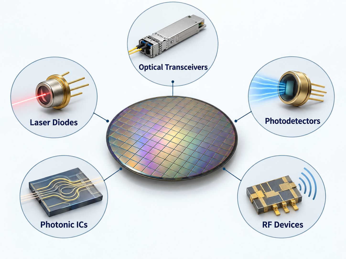
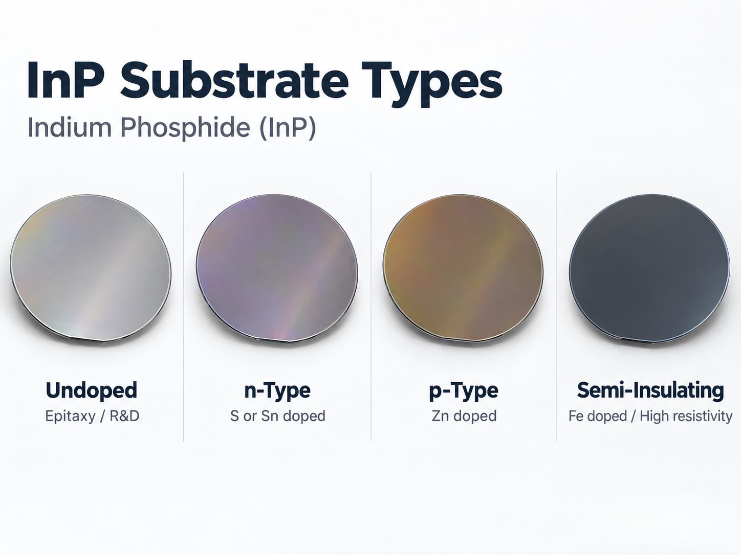
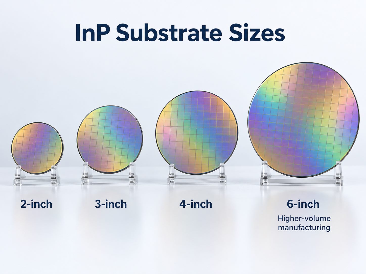
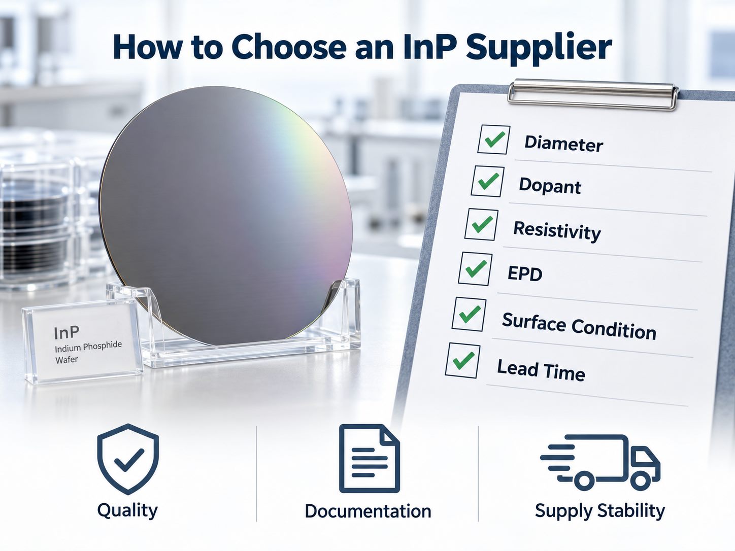
1. Indium Phosphide

Indium phosphide (InP) is a compound semiconductor material mainly used in high-frequency and optoelectronic devices.

It is commonly found in:

  • Optical communication systems
  • Photonic integrated circuits
  • Laser diodes
  • High-speed transistors
  • RF and microwave devices
  • Data-center optical modules

InP performs well in applications involving very high frequencies and light transmission.

Its supply chain is more specialized than conventional silicon. Crystal growth, wafer preparation, epitaxy, and device fabrication require dedicated processes, so production capacity cannot be expanded as easily as standard silicon manufacturing.

2. Photoresist

Photoresist in Semiconductor Manufacturing

Photoresist is a photosensitive material used during semiconductor lithography. A thin layer is coated onto the wafer and exposed through a patterned mask. After development, the remaining resist defines where later processes such as etching, deposition, or implantation will take place.

As circuit geometries shrink, photoresist must provide tight control over:

  • Resolution
  • Film uniformity
  • Sensitivity
  • Purity
  • Defect density
  • Line-edge accuracy

Photoresist is also used in PCB fabrication to define copper circuitry. The basic concept is similar, although semiconductor lithography operates at a much finer scale and under much stricter contamination requirements.

3. Silicon Carbide

Silicon Carbide in Power Electronics

Silicon carbide (SiC) is a wide-bandgap semiconductor material widely used in high-power electronics.

It is particularly suitable for systems that operate at high voltage, high temperature, or high switching frequency.

Typical applications include:

  • EV traction inverters
  • On-board chargers
  • DC-DC converters
  • Fast chargers
  • Solar inverters
  • Industrial motor drives
  • Data-center power supplies

SiC devices can reduce switching losses and improve power density, but manufacturing the wafers is difficult.

Crystal growth, slicing, polishing, epitaxy, and device processing all require precise control, which is one reason SiC supply has attracted attention as electric vehicles and power electronics expand.

4. Copper Foil

Copper foil is one of the core conductive materials used in PCB manufacturing.

After lamination and patterning, it becomes the board’s:

  • Signal traces
  • Power planes
  • Ground planes
  • Pads
  • Thermal structures

Copper thickness matters for current capacity, while surface roughness becomes especially important in high-frequency and high-speed designs.

Heavy copper boards need thicker copper for power handling and heat distribution. High-speed boards may require lower-profile copper to reduce conductor loss.

Although copper foil sounds like a basic material, its thickness, roughness, adhesion, and mechanical properties can directly affect PCB performance.

5. Tantalum Capacitors

Tantalum capacitors are electronic components rather than semiconductor raw materials, but they still matter in the wider electronics supply chain.

They are used where designers need relatively high capacitance in a compact package, including:

  • Power filtering
  • Industrial electronics
  • Telecom equipment
  • Aerospace systems
  • Medical devices
  • Automotive electronics

For PCBA production, a small passive component can become a bottleneck.

If a qualified tantalum capacitor is unavailable, replacing it may require checking voltage rating, capacitance, ESR, package size, reliability requirements, and approved alternatives before assembly can continue.

6. ABF Substrates

ABF substrates are widely used in advanced semiconductor packaging.

ABF stands for Ajinomoto Build-up Film, an insulating material used in high-density package substrates.

These substrates create the electrical connection between fine-pitch semiconductor packages and the larger interconnect structures on the PCB.

They are commonly associated with:

  • CPUs
  • GPUs
  • AI accelerators
  • Networking processors
  • High-performance computing devices

As package I/O density increases, substrate routing becomes finer and more complex.

Wafer capacity alone therefore does not determine how many finished chips can enter the market. Advanced packaging and substrate availability can become separate constraints.

7. High-Purity Nitrogen

Nitrogen is common in industry, but semiconductor manufacturing requires very high purity and controlled delivery.

It is used for:

  • Equipment purging
  • Oxygen displacement
  • Wafer handling
  • Chamber protection
  • Drying
  • Controlled process atmospheres

Semiconductor processes are highly sensitive to contamination, so trace moisture, particles, oxygen, or chemical impurities can affect process stability and yield.

High-purity nitrogen also has a place in electronics assembly. Nitrogen-assisted reflow and soldering processes may be used when oxidation control is important.

8. MLCCs

Multilayer ceramic capacitors, or MLCCs, are among the most common passive components on modern PCB assemblies.

They are used for decoupling, filtering, bypassing, and power stabilization.

Supply becomes more sensitive when a design combines demanding requirements such as:

  • Very small package sizes
  • High capacitance
  • Higher voltage
  • Automotive qualification
  • Tight tolerance
  • Specific temperature characteristics

An MLCC with the same nominal capacitance is not always a direct substitute.

Engineers may also need to review dielectric type, DC bias behavior, package size, voltage rating, temperature coefficient, and qualification requirements before approving an alternative.

9. Molybdenum Sputtering Targets

Molybdenum sputtering targets are used in physical vapor deposition processes.

During sputtering, atoms are released from the target and deposited as a thin film onto another surface.

For semiconductor and electronic applications, target quality depends on more than the molybdenum itself.

Manufacturers need to control:

  • Material purity
  • Density
  • Grain structure
  • Contamination
  • Dimensional consistency
  • Bonding quality

Minor impurities that are acceptable in ordinary industrial metal may create problems during high-precision thin-film processing.

Semiconductor-grade sputtering targets therefore belong to a highly controlled specialty-material supply chain.

10. Electronic-Grade Sulfuric Acid

Sulfuric acid is widely used in industry, but semiconductor production requires ultra-high-purity electronic-grade material.

It is used in wafer cleaning and other chemical processes where trace contamination must remain tightly controlled.

Key concerns include:

  • Metallic impurities
  • Particles
  • Organic contaminants
  • Ionic contamination

Producing industrial sulfuric acid and producing semiconductor-grade sulfuric acid are very different manufacturing tasks.

The purification system, packaging, transportation, handling, and quality controls all need to meet semiconductor processing requirements.

11. High-End PCB Substrates

After a semiconductor is packaged, it still needs a circuit board capable of supporting its electrical and thermal requirements.

Standard FR-4 is suitable for many products, but high-speed, RF, automotive, computing, and industrial designs may need laminates with tighter control over:

  • Dielectric constant
  • Dissipation factor
  • Tg
  • Thermal expansion
  • Moisture absorption
  • Dimensional stability
  • Copper adhesion

For these boards, material selection is part of the engineering process.

A laminate with similar mechanical specifications may behave very differently at multi-gigabit data rates or during repeated thermal cycling.

12. Electronic-Grade Glass Fiber Cloth

Electronic-grade glass fiber cloth is a reinforcement material used in many PCB laminates.

The cloth is impregnated with resin to form prepreg, which is then laminated with copper foil and core materials to build the PCB structure.

Important properties include:

  • Cloth thickness
  • Weave style
  • Yarn size
  • Resin impregnation
  • Dimensional stability
  • Surface uniformity

Glass weave can also affect high-speed signal behavior.

At very high data rates, traces passing over different glass and resin regions can experience small variations in effective dielectric properties. Material selection, routing strategy, and spread-glass constructions can help control this effect.

How Do Semiconductor Material Constraints Affect PCB and PCBA Production?

Before a finished electronic product can be built, the project depends on PCB materials, passive components, connectors, assembly materials, and manufacturing capacity.

Several materials discussed above connect directly with PCB and PCBA production:

  • Copper foil affects conductor construction and electrical performance.
  • Glass cloth and laminate systems influence PCB mechanical and dielectric properties.
  • MLCCs and tantalum capacitors affect BOM availability and assembly scheduling.
  • High-performance substrates become more important as signal speed and power density increase.

Sourcing and engineering therefore need to work together in complex PCB and PCBA projects, particularly when materials or components have limited qualified alternatives.

Which Materials Matter Most in PCB Manufacturing?

Key Materials in PCB Manufacturing

For PCB fabrication, the most relevant items from the list are copper foil, laminate materials, and electronic glass cloth.

Together, these materials define much of the board’s electrical, mechanical, and thermal behavior.

Engineers may need to evaluate:

  • Dk and Df
  • Tg and thermal stability
  • CTE
  • Copper thickness
  • Copper roughness
  • Moisture absorption
  • CAF resistance
  • Dimensional stability

These parameters become more important in HDI, RF, high-speed, high-current, heavy copper, automotive, and other demanding boards.

For example, low-loss laminate may matter far more than standard FR-4 in high-speed interfaces, while copper thickness and thermal design become central in high-current power boards.

How Do Component Shortages Affect PCBA Assembly?

How Component Shortages Affect PCBA Assembly

A bare PCB can be fully manufactured and still sit idle if critical BOM components are missing.

Component availability should therefore be reviewed early, especially for parts that are difficult to substitute.

Important checks include:

  • Manufacturer part number
  • Package and footprint
  • Lifecycle status
  • Lead time
  • Approved alternatives
  • Electrical specifications
  • Reliability grade
  • Supply continuity

Passive components deserve attention as well.

An MLCC or tantalum capacitor may look simple, but replacement can require engineering approval when voltage, dielectric behavior, package size, temperature performance, or qualification requirements differ.

How Can PCB and PCBA Buyers Reduce Supply-Chain Risk?

The practical approach is to identify critical materials and components before production starts.

For PCB projects, buyers should clearly define material, stack-up, copper thickness, impedance, surface finish, and any special thermal or reliability requirements.

For PCBA projects, the BOM should include accurate manufacturer part numbers and approved alternatives where possible.

Several steps can improve sourcing flexibility:

  • Perform DFM and BOM review early.
  • Approve equivalent PCB materials where technically acceptable.
  • Identify long-lead-time and single-source components.
  • Review alternative parts with engineering, not purchasing alone.
  • Separate ordinary BOM items from supply-critical parts.
  • Confirm material availability before mass production.

The goal is to avoid discovering a sourcing problem after production has already started.

How EBest Circuit Supports PCB and PCBA Manufacturing

How EBest Circuit Supports PCB and PCBA Manufacturing

At EBest Circuit, we support PCB and PCBA projects from engineering review and PCB fabrication through component sourcing, assembly, inspection, and testing.

Our PCB capabilities include:

  • Rigid PCB
  • Flex and rigid-flex PCB
  • HDI PCB
  • Heavy copper PCB
  • RF and microwave PCB
  • High-speed PCB
  • High-current PCB

For PCBA projects, EBest Circuit can also coordinate:

  • Component sourcing
  • SMT assembly
  • Through-hole assembly
  • Inspection
  • Testing

Before production, our engineering team can review key project information such as:

  • Gerber files
  • BOM
  • Pick-and-place data
  • PCB stack-up
  • Material requirements
  • Controlled impedance
  • Copper thickness
  • Assembly notes
  • Testing requirements

This allows PCB fabrication, component sourcing, and PCBA assembly requirements to be reviewed within the same project workflow.

Conclusion

These 12 materials and components show that semiconductor supply is closely tied to PCB and electronics manufacturing.

Some are used inside semiconductor fabrication. Others become important during advanced packaging, PCB production, component sourcing, and PCBA assembly.

For PCB and PCBA buyers, the practical issue is broader than chip availability. PCB materials, BOM components, fabrication requirements, assembly, and sourcing all need to align before a product can move smoothly into production.

If you have a PCB or PCBA project, send EBest Circuit your Gerber files, BOM, stack-up, and technical requirements for engineering review and quotation.

You may also like

W-Band Antenna PCB: Design, Materials, Testing and Manufacturing

August 19th, 2026

A W-band antenna PCB integrates, feeds, packages or interconnects an antenna system operating in the W-band, commonly treated as 75-110 GHz. At these frequencies, laminate behavior, copper geometry, registration, transitions, assembly and test fixtures can change electrical performance, so the board must be designed and manufactured as part of the RF system rather than as a conventional interconnect.

The right implementation may be an etched antenna, a phased array, a substrate-integrated waveguide (SIW) structure, an antenna-in-package interface or a hybrid PCB-to-waveguide assembly. There is no universal stackup or trace dimension for every project. Electrical models, mechanical interfaces, fabrication limits and validation methods must be agreed for the actual design.

Realistic W-band antenna PCB with integrated array and RF feed structures

What Is a W-Band Antenna PCB?

A W-band antenna PCB is a frequency-sensitive circuit structure in which the board participates directly in radiation, RF feeding, beamforming, packaging or transition to another transmission medium. Small dimensional changes that are harmless at lower frequencies can create measurable phase, loss or impedance differences in W-band channels.

The term does not describe one fixed antenna shape. A PCB can carry a single radiating element, a corporate-feed network, a multi-channel array, SIW cavities, launch structures or the interface between a chipset and a waveguide antenna. A practical “mmwave pcb antenna” design therefore begins by defining which electromagnetic functions belong to the PCB and which belong to the package, connector, waveguide or surrounding enclosure.

W-band projects usually require closer coordination among antenna designers, package engineers, PCB fabricators, assemblers and test engineers. Their models must use compatible material assumptions, reference planes and mechanical dimensions; otherwise a board can meet its drawing yet miss the system target.

Where Are W-Band Antenna PCBs Commonly Used?

W-band antenna PCBs are used where compact antennas, short wavelengths, wide available bandwidth or fine angular resolution justify the added design and validation effort. The exact frequency allocation and product rules depend on the application and region, so the system specification should define the intended operating window.

Common engineering contexts include:

  • short-range and multi-gigabit wireless links;
  • imaging, sensing and research instruments;
  • phased-array and beam-steering platforms;
  • radar development above conventional automotive radar bands;
  • frequency-extender, calibration and laboratory evaluation hardware;
  • compact modules that transition between silicon, PCB and waveguide structures.

Which W-Band Antenna Type Is Best for Your PCB Project?

The best antenna type is the one that meets the radiation, bandwidth, packaging and manufacturing targets with a testable interface. A simple etched structure may reduce part count, while an array, SIW or antenna-in-package approach can better support gain, integration or feed control at the cost of added process sensitivity.

Architecture Typical fit Main manufacturing concern
Etched patch or slot Compact single element or small array Etch geometry, copper profile, dielectric thickness and surrounding metal
Corporate-fed array Higher gain or controlled beam pattern Feed symmetry, cumulative phase error and registration across channels
SIW or PCB waveguide Low-profile guided structures and transitions Via placement, cavity dimensions, plating and launch repeatability
Antenna-in-package Short chip-to-antenna path and dense integration Package-to-board transition, assembly alignment and warpage
Hybrid PCB-to-waveguide System connection to horn or metal waveguide Mechanical datum, aperture alignment, surface contact and fixture repeatability

A “w band patch antenna” can be suitable when its bandwidth, gain and installation environment are compatible with a planar radiator. A “w-band antenna array” is more appropriate when the system needs higher effective aperture or beam steering, but the additional channels make material variation, conductor geometry and assembly alignment harder to control.

What Should Be Confirmed Before W-Band Antenna PCB Design?

Confirm the RF, mechanical, material and validation boundaries before committing the layout. The project should not begin with a generic 50-ohm trace assumption because the usable geometry depends on the transmission structure, laminate construction, copper profile and surrounding reference planes.

The design team should establish:

  • operating frequency range, channel plan and required bandwidth;
  • antenna architecture, polarization, gain and scan requirements;
  • chipset, package, connector, waveguide and enclosure interfaces;
  • material family, target dielectric properties and allowed construction options;
  • stackup, copper profile, conductor definition and registration assumptions;
  • simulation reference planes and de-embedding approach;
  • acceptable amplitude, phase, impedance and radiation-pattern criteria;
  • prototype quantity, assembly state and planned validation stages.

These inputs do not need to become a long document checklist. They need to be consistent. A model based on one dielectric thickness or copper treatment cannot reliably predict a board manufactured with another construction.

How Should a W-Band Antenna Be Placed and Routed on the PCB?

Place the antenna and its feed network as a controlled electromagnetic region, not as ordinary signal routing. Keep the layout consistent with the simulated stackup, reference planes, enclosure and launch geometry, and protect the antenna aperture from copper, components and mechanical features that were absent from the model.

Useful layout controls include:

  • keeping feed paths short, geometrically consistent and free of unplanned neck-downs;
  • preserving the intended ground return and avoiding reference-plane discontinuities;
  • using symmetric routing where array channels require matched phase and amplitude;
  • locating via fences and SIW rows from the electromagnetic design, not from a generic spacing rule;
  • defining copper keepouts around radiating elements and transitions;
  • placing mounting holes, shields, fasteners and enclosure walls in the simulation model;
  • avoiding solder mask or surface treatments over critical RF regions unless the design explicitly includes them.

Via stitching can support ground continuity and field confinement, but more vias are not automatically better. Via diameter, pitch, antipad, plating and distance from the RF structure all affect the local field and manufacturability.

Which Materials and Stackups Affect W-Band Antenna Performance?

Materials and stackups affect W-band performance through dielectric constant, loss, thickness variation, moisture behavior, copper roughness, glass weave and construction repeatability. A material name alone is not enough; the design model should reflect the actual laminate, copper and fabrication construction being purchased.

Cutaway view of multilayer W-band antenna PCB materials, copper layers and via structures

Review these variables together:

  • design Dk and its test method at a relevant frequency;
  • dissipation factor and conductor-loss assumptions;
  • dielectric thickness and its manufacturing tolerance;
  • copper foil type, profile and plated thickness;
  • glass reinforcement or anisotropy when present;
  • bondply, prepreg or adhesive behavior in a hybrid stackup;
  • dimensional stability through lamination and subsequent thermal cycles;
  • surface finish and solder mask interaction with exposed RF conductors.

Low nominal Df does not guarantee low insertion loss if rough copper, long feeds or poor transitions dominate. Likewise, two laminate constructions with similar datasheet Dk values may produce different effective impedance and phase when their reinforcement, resin content or copper profile differs. For a broader material context, see our RF Microwave PCB guide.

How Do Feed Lines, Impedance Matching, Vias and Transitions Affect Performance?

Feed lines and transitions determine how much of the generated W-band energy reaches the antenna with the intended amplitude and phase. The whole path must be modeled across launches, vias, package pads, cavities, connectors and waveguide interfaces; checking only a straight transmission-line coupon leaves the most sensitive discontinuities untested.

At W-band, a transition can add loss or resonance through a small pad, antipad, stub, air gap or registration shift. Channel-to-channel differences can also accumulate through small length and geometry variations. The design should therefore define the reference plane for every reported result and distinguish simulated antenna impedance from the impedance seen through the complete feed and fixture.

Impedance control PCB principles still apply, but a conventional coupon may not represent the antenna feed, via transition or package launch. Use dedicated test structures when the project needs to separate material, line, transition and fixture effects.

What Is the W-Band Antenna PCB Design and Manufacturing Process?

The process should connect electromagnetic design, fabrication engineering and staged verification so that production data preserve the modeled structure. The PCB fabricator should review the stackup and critical geometry before release, while the antenna designer retains responsibility for RF synthesis and system-level performance.

Engineer inspecting a high-frequency antenna PCB under an optical measurement microscope
  1. Define the operating band, antenna architecture, interfaces and validation targets.
  2. Select a manufacturable material system and build the preliminary stackup.
  3. Simulate the antenna, feed network, transitions, package and nearby mechanical features.
  4. Add fabrication tolerances to sensitivity analysis instead of validating only nominal geometry.
  5. Complete PCB DFM review for conductor definition, registration, drilling, plating and lamination.
  6. Fabricate coupons or representative test structures with the prototype panel.
  7. Inspect the bare board before assembly and record actual stackup or dimensional results where required.
  8. Assemble with controlled alignment, reflow profile, flatness and handling conditions.
  9. Measure interconnect behavior and antenna performance using agreed reference planes.
  10. Correlate test results with the model before freezing the production build.

A useful “mmwave pcb design guide” must include this feedback loop. If the prototype fails, the team needs enough coupon, dimensional and fixture data to identify whether the cause is the antenna model, the feed path, fabrication variation, assembly or measurement setup.

Why Does a W-Band Antenna PCB Show High Loss, Weak Gain or Phase Error?

High loss, weak gain and phase error usually come from several interacting sources rather than one obvious defect. Diagnose the signal path in stages and compare nominally identical channels before changing the antenna geometry.

Symptom Likely cause group First check
Higher insertion loss Material loss, copper roughness, long feed or transition loss Compare line and transition test structures before OTA testing
Resonance shifted Dielectric thickness, effective Dk, etch geometry or nearby metal Measure critical dimensions and confirm the built stackup
Weak or distorted pattern Feed imbalance, enclosure interaction, assembly obstruction or fixture scattering Repeat with the agreed mechanical configuration and calibration boundary
Channel phase spread Line-length, weave, copper, registration or package variation Compare matched channels through the same fixture and reference plane
Poor repeatability Connector torque, waveguide alignment, contact, cable movement or calibration drift Re-seat the fixture and run a repeatability study

Do not tune the board from a single unverified measurement. First confirm calibration, fixture repeatability and reference-plane location. Then compare bare-board dimensions, material construction and assembly state against the model.

How Should a W-Band Antenna PCB Be Tested Before Production?

Test a W-band antenna PCB in layers: bare-board quality, RF interconnect behavior and over-the-air antenna performance answer different questions. A PCB supplier can verify fabrication features and agreed electrical structures, but antenna gain and radiation pattern require suitable W-band equipment, fixtures and an OTA method.

W-band antenna PCB mounted in a millimeter-wave laboratory test fixture

A practical validation sequence may include:

  • visual and dimensional inspection of critical conductors, apertures and registration;
  • microsection or construction verification for selected vias and layer relationships;
  • continuity, isolation and agreed impedance or transmission-line coupons;
  • line and transition measurements with defined calibration and de-embedding;
  • channel-to-channel amplitude and phase comparison for arrays;
  • assembled-module checks with the final package, connector or waveguide interface;
  • OTA return loss, gain, pattern, polarization and scan testing when the responsible laboratory capability is confirmed.

W-band characterization commonly uses frequency extenders and waveguide hardware. Fixture design, flange alignment and calibration boundaries must be documented because a fixture error can look like a PCB or antenna defect.

How Do Assembly and Packaging Affect W-Band Antenna Performance?

Assembly and packaging affect W-band performance by changing alignment, standoff, flatness, local dielectric loading and transition geometry. A bare board that matches its drawing can still perform differently after a chipset, shield, radome, heat spreader or waveguide block is installed.

Control the assembly variables that are included in the RF model:

  • package placement and rotation relative to feed structures;
  • solder volume, collapse and standoff for flip-chip or fine-pitch interfaces;
  • board and package warpage through reflow;
  • underfill, adhesive or coating near active RF regions;
  • connector or waveguide flange alignment and fastener sequence;
  • shield, enclosure and absorber position;
  • cleanliness and surface contamination around exposed conductors.

If assembly is outsourced separately from PCB fabrication, provide the assembler with the RF-sensitive keepouts and mechanical datums. Standard placement tolerances may not describe the relative alignment that the antenna transition actually needs.

What Factors Affect W-Band Antenna PCB Cost?

W-band antenna PCB cost is driven by material choice, stackup complexity, tolerance control, prototype learning and validation—not by board area alone. Early agreement on which characteristics are truly critical can prevent unnecessary controls while protecting RF performance.

The main cost drivers are:

  • specialty laminate availability and minimum purchase quantities;
  • hybrid or sequential lamination construction;
  • thin dielectric layers and tight thickness control;
  • fine conductor geometry, copper-profile requirements and etch compensation;
  • registration demands across antenna, feed and via structures;
  • small or dense plated holes, SIW rows and backdrilling when applicable;
  • dedicated coupons, dimensional reports, microsections or RF test structures;
  • assembly alignment, package complexity and special fixtures;
  • prototype iterations needed to correlate simulation and measured results;
  • production quantity, panel utilization and accepted yield window.

Cost should be reviewed against the validation plan. Removing a useful test structure may reduce initial panel cost but make a failed prototype harder to diagnose. Conversely, specifying a universal tight tolerance without sensitivity evidence can add cost without improving the antenna.

FAQ About W-Band Antenna PCB Projects

Is W-band always defined as 75-110 GHz?

75-110 GHz is a common engineering definition for the W-band, but applications, instruments and regulations may use narrower windows. State the exact operating range and channel plan in the project specification rather than relying only on the band name.

Can a w band patch antenna be fabricated as a conventional multilayer PCB?

It can use familiar PCB processes, but the construction may need tighter control of dielectric thickness, copper geometry, surface condition and registration than a conventional digital board. The antenna model must use the proposed stackup and manufacturing tolerances.

Which laminate properties matter most for a mmwave pcb antenna?

Design Dk, dissipation factor, thickness tolerance, copper roughness, reinforcement structure, moisture behavior and dimensional stability can all matter. Their relative importance depends on whether loss, phase consistency, resonance or mechanical stability dominates the design.

Does a PCB supplier validate antenna gain and radiation pattern?

Not automatically. A PCB supplier may inspect construction, dimensions and agreed RF coupons. Gain, radiation pattern, polarization and scan performance require suitable W-band fixtures and OTA equipment, so the responsible test party and acceptance method must be confirmed for each project.

What project information should be confirmed before production?

Confirm the operating range, antenna type, final stackup, named laminate, copper construction, critical geometry, mechanical interfaces, assembly state, quantity and acceptance method. Provide Gerber or ODB++ data plus relevant package or waveguide drawings when they are part of the manufactured interface.

Why can nominally identical antenna channels show different phase or gain?

Small differences in feed length, dielectric construction, glass weave, copper profile, registration, package alignment or fixture contact can accumulate across channels. Compare the channels through the same calibrated setup and inspect actual geometry before changing the design.

How Can EBest Circuit Support Your W-Band Antenna PCB Project?

EBest Circuit supports RF and high-frequency PCB manufacturing, impedance-controlled PCB work, impedance testing and engineering review for available high-frequency material systems. Because W-band performance depends on the exact stackup, copper construction, antenna topology, transitions and validation method, we review each design for manufacturability and sourcing feasibility rather than promise one universal process window.

Send the target frequency range, antenna architecture, Gerber or ODB++ data, stackup, material and copper requirements, critical tolerances, package or waveguide interface drawings, assembly information, quantity and RF acceptance plan to our engineering team at sales@bestpcbs.com. We can review the PCB manufacturing and assembly scope with your team. Antenna synthesis, W-band VNA measurement and OTA gain or pattern validation are included only when the responsible capability is confirmed for the specific project.

You may also like

Impedance Control PCB: Requirements, Stackup, and Testing

August 13th, 2026

An impedance control PCB can fail even when its Gerber files look correct. A changed dielectric thickness, an unclear reference plane, or an unapproved trace-width adjustment can move the finished impedance outside the required range. The result may be reflections, timing errors, excessive noise, or an interface that works in a prototype but fails after production changes.

The safest approach is to define the electrical target and manufacturing evidence before fabrication begins. This guide explains what customers should release, what a PCB manufacturer should confirm, and how stackup review, test coupons, and time-domain reflectometry (TDR) reports reduce avoidable production risk.

impedance control pcb
Impedance-controlled PCB fabrication connects the approved stackup with measurable production evidence.

What Is an Impedance Control PCB?

An impedance control PCB has one or more transmission lines manufactured to meet specified characteristic-impedance targets. Common examples include single-ended traces and differential pairs used for high-speed digital, communication, or RF signals.

Impedance is affected by the complete trace environment, not trace width alone. Important variables include:

  • Finished trace width and copper thickness
  • Spacing within a differential pair
  • Distance from the trace to its reference plane
  • Dielectric material, thickness, and design Dk
  • Solder mask and nearby copper geometry
  • Etching and lamination tolerances

A calculator can estimate a starting geometry, but the fabricated result depends on the manufacturer’s actual materials and processes. The released design should therefore identify the required impedance, tolerance, signal layers, reference layers, and controlled nets. The PCB supplier can then compare those requirements with the proposed production stackup.

The customer remains responsible for circuit function, interface requirements, signal-integrity targets, and final design approval. EBest Circuit (Best Technology) can review the released files for PCB manufacturability, coordinate a production stackup, fabricate the boards, and provide agreed impedance-testing evidence.

When Does a PCB Need Impedance Control?

Not every signal trace needs controlled impedance. The decision depends on signal edge rate, interconnection length, interface requirements, acceptable reflection, and the complete electrical path. Clock frequency alone is not enough to make the decision.

Customers should evaluate impedance control when a board includes high-speed digital interfaces, RF paths, fast clock or memory signals, antenna feeds, or other transmission lines whose reflections could reduce operating margin. The applicable component and interface specifications should define the required targets.

Skipping control to reduce board cost can create a larger loss later. Possible consequences include:

  • Prototype-to-production performance changes
  • Intermittent communication errors
  • Reduced eye opening or timing margin
  • Excessive ringing, overshoot, or radiated noise
  • Repeated layout changes without proof that fabrication was the cause

The practical decision is not simply “high-speed board or ordinary board.” Identify which nets require control, the target for each net group, and the evidence needed for acceptance. Do not mark every trace as controlled when only a small number of critical nets require it; unnecessary requirements can increase engineering work, coupon space, testing, and cost.

PCB Impedance Control Requirements

An RFQ that says only “impedance control required” leaves essential decisions unresolved. Before quotation or engineering release, provide a controlled-impedance table or equivalent fabrication note that connects each target to specific layers and net classes.

The release package should state:

  • Target impedance for every controlled net class
  • Whether each target is single-ended or differential
  • Required tolerance, such as the project-approved percentage or ohmic range
  • Signal layer and reference plane for each structure
  • Controlled net names or an unambiguous net-class identifier
  • Intended finished copper weight or thickness
  • Approved material family and any required Dk basis
  • Finished board thickness and stackup constraints
  • Whether impedance coupons and TDR reports are required
  • Whether the manufacturer may adjust trace width or spacing

The Gerber or ODB++ data, fabrication drawing, stackup table, net information, and impedance notes must agree. If one file specifies a 100-ohm differential pair while another calls for 90 ohms, fabrication should stop for clarification rather than rely on an assumption.

Customers should also define the approval path. For example, can the PCB manufacturer compensate a finished trace width to suit its etching process? Can it propose a different prepreg while maintaining the approved dielectric thickness and impedance? Which changes require written customer approval? Resolving these questions before CAM release helps prevent untracked changes and repeated quotation cycles.

Controlled Impedance PCB Layer Stackup

The layer stackup connects the electrical model to the material that will be laminated. A nominal layer count and overall thickness are not enough. The manufacturer needs the copper distribution, core and prepreg construction, finished dielectric thicknesses, material data, and reference-plane relationships.

For each controlled structure, confirm:

  • Whether it is a surface microstrip, embedded microstrip, stripline, or coplanar structure
  • Which plane provides the continuous reference
  • The finished dielectric thickness between the signal and reference layers
  • The finished trace width, copper thickness, and differential spacing
  • Whether solder mask is included in the calculation
  • The material Dk value and frequency basis used for modelling
  • Whether nearby copper, plane openings, or routing transitions disturb the structure

A standard stackup can shorten engineering time, but it should not be accepted only because its layer count and board thickness match the design. The available trace geometry must also fit the customer’s routing density and manufacturing limits.

The customer should review the supplier’s proposed production stackup before fabrication. If the supplier changes dielectric thickness or material construction, the calculated line geometry may also need to change. Keep the approved stackup, impedance table, and revised production files under the same revision so purchasing, engineering, and quality teams evaluate one controlled release.

impedance control pcb
CAM and stackup review align controlled traces with available materials and production geometry.

Impedance Control in PCB Manufacturing

Manufacturing converts the approved model into actual copper and dielectric geometry. Lamination, material variation, copper plating, imaging, and etching all influence the finished result. That is why a theoretical value from the design stage cannot, by itself, prove production conformity.

During engineering review, the PCB manufacturer should compare the customer’s targets with the proposed stackup and process capability. If compensation is necessary, the supplier should return the proposed production geometry for approval instead of silently changing controlled features.

Typical manufacturing controls include:

  • Material and stackup verification before lamination
  • CAM checks for controlled nets, reference planes, and coupon structures
  • Process compensation based on the supplier’s qualified etching data
  • Finished-copper and geometry control
  • Coupon fabrication on the same production panel under representative conditions
  • TDR measurement against the agreed target and tolerance
  • Traceable reporting linked to the job, lot, or panel as agreed

Coupon placement and design should represent the relevant production structures. A coupon is useful only when its layer, reference plane, geometry, materials, and processing are representative of the controlled traces being accepted.

If a measured coupon is outside the specified tolerance, the correct response depends on the agreed acceptance plan. The manufacturer should contain the affected material, review the stackup and process data, and communicate the finding before shipment. The customer should decide whether further investigation, rework, rebuild, or a documented deviation is acceptable.

impedance control pcb
A representative impedance coupon can be measured by TDR against the approved target and tolerance.

How to Check Impedance on PCB?

The most common production method is TDR testing of an impedance coupon. The instrument sends a fast electrical transition into the test structure and evaluates reflections along the transmission path. The result is compared with the approved target and tolerance.

Before accepting a test report, check that it identifies:

  • Customer part number and revision
  • Manufacturing job, lot, or panel reference
  • Coupon or test-structure identification
  • Controlled structure and target impedance
  • Required tolerance or acceptance limits
  • Measured result for each reported structure
  • Test date, equipment, or method when required by the quality plan
  • Clear pass/fail status and authorized review

A report showing only one impedance number without identifying the structure or job may not be sufficient for traceability. Likewise, a passing coupon does not prove the performance of the complete assembled product. It demonstrates that the representative PCB structure met the agreed impedance acceptance criteria.

Customers with stricter reliability or compliance needs should define the sampling plan, report format, retention period, and any coupon-storage requirement in the purchase documentation. If direct board measurements, network analysis, or product-level signal-integrity testing are needed, those requirements should be specified separately because they are not automatically included in standard coupon testing.

A Practical Impedance Control PCB Example

Consider a multilayer control board containing a high-speed differential interface and several single-ended clock lines. The initial RFQ includes Gerber files and an overall board thickness, but it does not identify the controlled nets, reference planes, tolerance, or required report.

If fabrication begins from that package, different suppliers may choose different dielectric constructions and compensate the traces differently. The boards may all match the visible artwork while producing different impedance results.

A safer release would include:

  • A table listing each controlled net class and target
  • The approved layer and reference-plane assignments
  • A preliminary stackup with material and thickness constraints
  • Permission boundaries for trace-width or spacing adjustment
  • A requirement for representative coupons and a TDR report
  • A named customer approver for stackup or geometry changes

EBest Circuit (Best Technology) can review this package against available PCB materials and fabrication rules. If the proposed stackup requires a geometry adjustment, the revised values can be returned for customer approval before production. After fabrication, the agreed coupon results can be supplied with the manufacturing record.

This process does not transfer circuit-design ownership to the manufacturer. It gives both parties a controlled handoff: the customer defines the electrical requirement, the manufacturer defines how the approved requirement will be produced and verified, and unresolved differences are closed before material is committed.

FAQs About Impedance Control PCB

Does every high-speed PCB require impedance control? Not automatically. The customer should evaluate signal edge rate, interconnection length, interface specifications, and acceptable reflection. Control the nets whose transmission-line behaviour can affect performance.

What impedance tolerance should I specify? Use the tolerance required by the interface, design analysis, and product acceptance plan. Confirm that the selected PCB construction and supplier process can support it before release; do not assume one tolerance fits every design.

Can a PCB manufacturer change controlled trace width? Only within the agreed approval process. Manufacturing compensation may be necessary, but the proposed finished geometry and stackup should be reviewed when the change could affect routing, clearance, coupling, or signal performance.

Does a passing TDR coupon guarantee that the assembled product will work? No. It verifies the representative PCB structure against the agreed impedance criteria. Component models, connectors, vias, layout transitions, assembly, firmware, and system conditions still affect final performance.

What should I send for an impedance control PCB quotation? Send the fabrication data, drawing, stackup constraints, controlled-net table, impedance targets and tolerances, material requirements, finished thickness and copper requirements, coupon/report expectations, quantity, and revision. For a manufacturing review or quotation, contact sales@bestpcbs.com.

You may also like

Microvia Aspect Ratio: Calculate It Before PCB Release

August 10th, 2026

Microvia aspect ratio can look acceptable in a PCB layout while still creating manufacturing risk. If the microvia is too deep for its diameter, drilling, plating, filling, and bonding margin decreases. The result may be a stackup change, lower yield, or failure during thermal cycling.

This guide explains how to calculate the ratio from the actual stackup and prepare the right information for fabricator review. EBest Circuit (Best Technology) can support PCB manufacturability review, HDI fabrication, sourcing, PCBA, and agreed inspection and testing. The customer owns circuit performance, released files, and final acceptance criteria.

microvia aspect ratio
Microvia Aspect Ratio

What Is Microvia Aspect Ratio?

Microvia aspect ratio describes the relationship between the depth of a microvia and its diameter. In its simplest form:

Microvia aspect ratio = microvia depth ÷ microvia diameter

For example, a 75 μm deep microvia with a 100 μm diameter has an aspect ratio of 0.75:1. A 100 μm deep microvia with the same diameter has a ratio of 1:1.

Confirm the fabricator’s conventions before calculating:

  • Does depth mean dielectric distance only, or does it include relevant copper?
  • Does diameter mean the drilled opening or finished opening?
  • Do CAD, fabrication drawings, and CAM use the same values?

IPC-linked definitions commonly use a maximum ratio of 1:1 and total depth of 0.25 mm. This identifies the structure; it does not guarantee that every 1:1 design is easy to produce or reliable.

Calculating early prevents the team from completing BGA escape routing around a hole geometry that cannot be produced with enough margin.

microvia aspect ratio
HDI PCB layer structure with a copper-plated microvia

How Do You Calculate Via Aspect Ratio?

Start with the production stackup, not the nominal finished board thickness. A through-hole via crosses most or all of the board, but a laser microvia normally connects a much shorter layer span. Its depth should therefore be taken from the actual build-up dielectric and land construction for that layer pair.

Use this calculation sequence:

  • Identify the microvia start and stop layers.
  • Record the actual dielectric thickness between the relevant lands.
  • Confirm whether the fabricator includes outer or target copper in the depth calculation.
  • Confirm whether the denominator is the drilled opening or finished diameter.
  • Divide the confirmed depth by the confirmed diameter.
  • Repeat the calculation for every microvia family rather than assuming one value covers the entire board.

Example: an L1–L2 microvia with an 80 μm depth and 100 μm diameter is 0.8:1. A second layer pair with a 100 μm depth and the same diameter is 1:1. Calculate them separately even if their CAD pad stacks look identical.

Record the result beside the drill definition or stackup note so every reviewer uses the same geometry.

What PCB Aspect Ratio Is Suitable for Microvias?

No single production number suits every PCB. Check the ratio against:

  • Material and dielectric tolerance.
  • Via profile and target-pad preparation.
  • Plating, filling, and lamination capability.
  • Assembly exposure and reliability requirements.

A 1:1 ratio is widely cited in IPC-linked definitions. Industry guidance often prefers about 0.75:1 or below because a shallower, wider structure gives drilling, plating, and filling more margin. These are design references, not universal guarantees.

Treat the ratio as a decision gate:

  • Below the supplier’s established production target: proceed with normal DFM confirmation.
  • Near the supplier’s limit: review tolerances, via profile, plating, fill, registration, and reliability evidence.
  • Above the supplier’s confirmed limit: increase the diameter, reduce the dielectric depth, or change the HDI construction before release.

Confirm that any published maximum applies to the selected material, copper, quantity, and inspection level. Prototype feasibility is not automatically a production rule.

How Does Microvia Size Change the Result?

For a fixed depth, a smaller diameter increases the ratio and reduces process margin. Use the largest microvia that still completes the required escape routing.

Consider an 80 μm depth:

Microvia diameter Calculated ratio Design implication
125 μm0.64:1Wider geometric margin, if pad and routing space allow
100 μm0.80:1Requires confirmation against the selected process
80 μm1.00:1At the commonly cited definition limit and needs close review

Also confirm:

  • Capture and target-pad size.
  • Registration tolerance and BGA pitch.
  • Via-in-pad treatment and copper filling.
  • Component pitch, fanout approach, and affected layer pairs.

EBest Circuit can review manufacturability and assembly interfaces. The customer retains responsibility for component selection, electrical fanout, and the released layout.

How Do You Check Blind Via Aspect Ratio?

First identify whether the feature is a laser microvia or a mechanically drilled blind via. They use different processes and may use different ratio conventions.

For a laser blind microvia, use the controlled depth of its specific build-up layer pair. For a mechanically drilled blind via spanning a thicker section, use the actual controlled drilling depth and the diameter convention stated by the fabricator. Do not calculate either feature from the full board thickness unless it actually passes through that thickness.

Check these items together:

  • Via type and drilling method.
  • Start and stop layers.
  • Nominal and tolerance-controlled depth.
  • Drilled and finished diameter definitions.
  • Capture and target-pad dimensions.
  • Filling, plugging, capping, or planarization requirements.
  • Sequential lamination stage.
  • Inspection and acceptance method.

This classification prevents quotation errors and late CAM questions about the required drilling process.

microvia aspect ratio
Microscope inspection of an HDI PCB microvia cross-section

When Should You Use a Via Aspect Ratio Calculator?

A calculator quickly flags via families moving toward a process limit. Use it:

  • During stackup planning.
  • Before BGA fanout is frozen.
  • After a dielectric or layer-pair change.
  • Before design release.

A calculator cannot approve the design because it does not know the supplier’s actual process or the product’s reliability requirements. Use its result to trigger engineering review, not replace supplier confirmation.

Save the formula convention, source dimensions, layer pair, revision, and supplier response with the result.

microvia aspect ratio
Engineer reviewing HDI PCB stackup and microvia dimensions

Stacked Microvias vs Staggered Microvias

The main trade-off is:

  • Stacked microvias: save routing area but add interfaces, filling, planarization, alignment, and sequential processing.
  • Staggered microvias: use more area but avoid placing every interface on one vertical load path.

Calculate every microvia level separately. Do not divide the full stack height by one hole diameter. Also review the interfaces, lamination count, filling, planarization, and required thermal-stress evidence.

Use stacked construction only when its density benefit is necessary and the fabrication and qualification plan supports it. Otherwise, staggered structures may offer a more controllable production path.

A Calculation Example Before PCB Release

Consider a compact control board with a fine-pitch BGA. The preliminary layout uses 80 μm laser holes through a 100 μm build-up depth. The calculated ratio is 1.25:1, which is above the commonly cited 1:1 microvia definition boundary and outside the comfortable range described by much industry guidance.

If routing is completed first, a later stackup change may affect impedance, BGA escape, cost, and delivery.

The engineering team evaluates three options:

  • Increase the laser diameter where the BGA pad and routing space allow.
  • Reduce the build-up dielectric depth using an approved manufacturable stackup.
  • Change the layer-transition strategy, including selective use of staggered structures.

The team selects a 100 μm hole with an 80 μm depth, producing 0.8:1. Before freezing the layout, it sends the revised stackup, drill table, pad geometry, fill requirement, impedance information, and reliability expectations to the fabricator.

This is an illustrative scenario. The key sequence is:

  • Calculate the ratio.
  • Compare it with the supplier’s process window.
  • Revise before routing is frozen.
  • Document supplier confirmation.

What Should You Send for DFM Review?

A manufacturer cannot confirm feasibility from the ratio alone. The review package must show the complete PCB construction and acceptance needs.

Prepare these files and decisions:

  • Gerber or ODB++ data and NC drill files.
  • Controlled stackup with layer numbers and dielectric thicknesses.
  • Drill table identifying every via family and start/stop layer.
  • Drilled versus finished diameter convention.
  • Copper weights and plating requirements.
  • Pad stacks, target lands, and critical BGA footprints.
  • Via-in-pad filling, capping, and planarization requirements.
  • Impedance requirements and test-coupon needs.
  • Material requirements and acceptable alternatives.
  • Prototype and production quantities.
  • Inspection, thermal-stress, electrical-test, and acceptance requirements.
  • BOM and placement files if PCBA review is also required.

EBest Circuit (Best Technology) can use the released information to review PCB manufacturability, align fabrication and PCBA requirements, and coordinate agreed inspection or testing. If a value is still open, mark it as requiring supplier confirmation rather than allowing CAM assumptions to become an uncontrolled design decision.

For an HDI DFM review or PCB quotation, send the available project files and requirements to sales@bestpcbs.com.

FAQs About Via Aspect Ratio

Is 1:1 always a safe microvia aspect ratio?

No. It is commonly cited as an IPC-linked definition limit, but actual production suitability depends on materials, geometry, process controls, assembly exposure, and reliability requirements. Many design guides prefer additional margin below 1:1.

Should microvia depth include copper thickness?

Use the fabricator’s documented convention. Some calculations focus on dielectric depth, while others include relevant foil or land construction. Record the convention beside the result so every reviewer uses the same inputs.

Can one aspect ratio cover all microvias on a PCB?

Only if every microvia family has the same confirmed depth and diameter convention. Different layer pairs or stackup regions should be calculated separately.

Does a lower ratio guarantee microvia reliability?

No. A lower ratio generally improves geometric process margin, but material properties, target-pad preparation, copper deposition, fill quality, registration, lamination, assembly cycles, and qualification testing also matter.

When should the fabricator confirm the ratio?

Before the stackup and BGA fanout are frozen, and again after any change to dielectric thickness, hole size, copper construction, via type, or reliability requirement.

Need help checking your microvia aspect ratio before PCB release? Send your stackup, drill information, and available project files to sales@bestpcbs.com for DFM review and quotation support.

You may also like

Signal Transmission PCB Design, Prototyping and Assembly Services | Reliable Quality Control

July 31st, 2026

A reliable signal transmission PCB begins with one coordinated channel definition: driver edge rate, target impedance, stackup, trace geometry, return path, connectors, vias, termination, and acceptance testing. If any of these inputs changes after routing, the manufactured board may no longer match the simulation or interface requirement.

Identify interconnects whose electrical length, loss, coupling, or discontinuities can alter the received waveform. These paths need controlled geometry, documented fabrication assumptions, and verification from prototype through production.

Signal transmission PCB prototype in a controlled-impedance laboratory fixture

What Is a Signal Transmission PCB?

A signal transmission PCB controls waveform quality. The design must keep reflection, attenuation, skew, crosstalk, and EMI within the receiver’s margin. Traces, reference planes, vias, connectors, and termination therefore form one electrical structure.

The board may carry digital links, clocks, memory buses, video, Ethernet, USB, LVDS, RF, or precision analog signals. Risk depends on edge rate, channel length, loss budget, receiver margin, and return-path geometry. A low clock frequency can still cause transmission-line behavior when its driver edge is fast.

Check these three structures before classifying a route as controlled:

  • Signal conductor: Define the routing layer, finished width, copper thickness, pair spacing, maximum skew, and every pad or via transition.
  • Dielectric system: Define the pressed dielectric thickness, design Dk and Df, glass construction, copper profile, and allowed material equivalents.
  • Return path: Name the reference layer, prohibit split or void crossings, and provide a return transition beside each signal-layer change.

Minimum release evidence: The fabrication package should contain a controlled-net table, approved stackup, impedance targets and tolerances, coupon requirements, and the required test-report format. Without these items, the supplier cannot verify that the manufactured structure matches the intended channel.

When Does a PCB Trace Behave as a Transmission Line?

Compare signal edge time with interconnect propagation delay. A trace needs transmission-line treatment when the signal can change substantially before the wave has propagated through the interconnect and returned. Use the driver’s fastest rise or fall time, not the protocol clock alone.

Calculate the boundary in five steps:

  1. Find the fastest edge. Use the maximum slew-rate condition from the datasheet, IBIS model, or measured source waveform. Include faster replacement parts if substitutions are allowed.
  2. Build the full electrical length. Include package escape, PCB trace, vias, connector, cable, branches, and receiver escape. Do not evaluate only the straight routed segment.
  3. Calculate one-way delay. Multiply each segment length by its modeled delay per unit length. Use the correct effective dielectric behavior for outer-layer and inner-layer structures.
  4. Compare delay with edge time. If the ratio is not clearly small, model the interconnect as a transmission line. Avoid a universal inch or frequency threshold because stackup and edge rate change the result.
  5. Apply the receiver limit. Check overshoot, undershoot, settling, jitter, eye opening, and input-protection limits. The receiver requirement determines whether the predicted discontinuity is acceptable.

Escalate uncertain routes to simulation. Use the production stackup, driver and receiver models, connector model, termination, and via geometry. The high-speed PCB design guide provides additional routing and stackup context. Record the model revision and acceptance limit so the result can support design release.

How Do Microstrip, Stripline and Coplanar Waveguide Structures Differ?

The structures differ mainly in field containment. Microstrip is an outer-layer trace, while stripline is embedded between reference planes. Coplanar waveguide adds grounded copper beside the signal on the same layer. The correct choice depends on routing access, loss, density, launch geometry, and fabrication tolerance.

Comparison dimension Microstrip Stripline Coplanar waveguide with ground
Trace location Outer layer over one main reference plane Inner layer between reference planes Usually outer layer with side grounds and a lower reference plane
Field exposure Partly in air and partly in dielectric Mostly contained within dielectric Shared among side grounds, lower plane, air, and dielectric
EMI and shielding More exposed to nearby structures Better field containment when planes remain continuous Good lateral field control when gaps and ground-via spacing are consistent
Inspection and probing Easy physical access Buried and not directly probeable Accessible, but side-ground geometry constrains probe and component placement
Manufacturing sensitivity Etch, plating, solder mask, and dielectric height Etch, core/prepreg thickness, resin flow, and layer registration Trace width, copper thickness, side gap, mask condition, and via-fence geometry
Typical use Short high-speed routes, accessible launches, antennas, and general controlled impedance Dense digital channels needing isolation and predictable reference planes RF launches and routes needing compact grounding or stronger field confinement
Main limitation Greater exposure and possible radiation or coupling More vias may be needed to reach components, adding discontinuities Small side gaps can be difficult to hold and may limit routing density

Selection rule: Use microstrip when access and a short launch matter; use stripline when isolation and field containment matter; use grounded coplanar waveguide when lateral grounding supports the launch. In every case, recalculate finished impedance with the actual mask, plating, etched shape, adjacent copper, and dielectric construction.

How Should Materials and Stackups Be Selected for Signal Transmission PCBs?

Start with the loss budget and a producible stackup. Signal transmission PCB material selection must account for impedance, routing density, frequency, temperature, and available constructions. Standard FR-4 suits many digital channels, but no universal frequency or data-rate limit makes every FR-4 construction acceptable.

Signal transmission PCB stackup and high-speed routing review with multilayer laminate sample

Use these five decisions to release the stackup:

  1. Set the channel limits. Define allowable insertion loss, return loss, delay, skew, temperature, voltage, and reliability.
  2. Assign every reference plane. Keep critical signal layers beside solid references and minimize plane changes.
  3. Use frequency-relevant material data. Confirm Dk, Df, test method, frequency, resin content, and glass style with the supplier.
  4. Check manufacturable geometry. Balance trace width and dielectric thickness against routing density, loss, and etch tolerance.
  5. Freeze the production stackup. Approve substitutions and require impedance recalculation before any material or construction change.

Choose the material by channel margin, not by data rate alone:

Check Standard FR-4 is suitable when Consider low-loss or hybrid when Confirm before release
Channel loss The modeled channel retains enough margin FR-4 loss consumes the available margin Channel length, spectrum, and insertion-loss limit
Dielectric data Available Dk and Df data match the design conditions Tighter high-frequency characterization is required Design Dk, Df, test method, frequency, and equivalents
Copper profile Conductor loss is not margin-critical Smoother copper is needed to reduce conductor loss Foil type, roughness model, and substitutions
Fabrication A standard, available construction meets the limits Hybrid bonding or dimensional behavior needs added control Prepreg compatibility, lamination plan, and qualification
Release evidence Simulation or prototype data confirms adequate margin Measured loss or phase limits justify the added material cost Correlation between the model and production stackup

Release rule: Use standard FR-4 when the modeled or measured channel keeps adequate margin. Specify low-loss laminate, smoother copper, or glass-weave controls only when they address a documented loss, skew, or phase risk.

How Should Controlled Impedance, Reference Planes and Return Paths Be Designed?

Design the signal conductor and return path as one structure. Signal transmission PCB impedance depends on the finished trace, dielectric, reference plane, nearby copper, and transitions. A width copied from a calculator is not a production specification.

  1. Define each impedance class. Record the net or net class, single-ended or differential target, tolerance, routing layer, reference layer, mask condition, and applicable interface requirement. Do not use one note for structures built on different layers.
  2. Lock a producible stackup. Confirm core and prepreg types, pressed dielectric thickness, finished copper, material Dk used for calculation, and permitted substitutions. Route only after the fabricator confirms that the proposed widths and gaps are manufacturable.
  3. Calculate finished geometry. Use a 2D field solver or a fabricator-validated model that includes etched trace shape, plating, solder mask, dielectric height, and adjacent copper. For differential pairs, solve width and spacing together because each trace couples to both its partner and the reference plane.
  4. Keep the reference continuous. Route critical traces over an unbroken plane. Keep them away from plane splits, antipad fields, board cutouts, connector voids, and plane edges that force return current around a longer loop.
  5. Provide a return path at layer changes. When a signal via changes layers but retains ground as its reference, place a ground stitching via near the signal transition. If the reference changes between different power or ground structures, define the high-frequency return path with the power-integrity design instead of assuming the planes are equivalent.
  6. Control discontinuities. Include connector launches, pads, neck-downs, test points, branches, AC-coupling capacitors, and vias in the channel model. Evaluate unused via stub length and use blind vias or backdrilling only when the predicted improvement justifies their cost and tolerance risk.
  7. Release verifiable data. Cross-check the impedance table against net names, stackup, drill files, layer order, and fabrication notes. Specify representative coupons and TDR reporting when production impedance evidence is required.

Use this release check for every controlled structure:

Control item Specify in the design package Failure prevented Verification
Single-ended trace Target, tolerance, layer, reference plane, width, and mask condition Reflection from incorrect finished impedance Field-solver result and representative TDR coupon
Differential pair Differential target, width, gap, pair skew limit, and reference Impedance error, timing mismatch, and common-mode conversion Coupled-field calculation and channel simulation where required
Reference plane Named reference layer and prohibited split, void, or edge crossings Return-path detour, crosstalk, and radiated emissions Layout review with both signal and plane layers visible
Layer transition Signal via, nearby return transition, antipad, and stub control Launch reflection and increased return-loop inductance 3D model or validated launch rule for sensitive channels
Fabrication release Approved stackup, finished copper, material rules, coupon, and report format Prototype-to-production geometry or material drift CAM review, impedance report, and controlled change approval

There is no universal trace width, pair gap, or return-via distance. Values must come from the released stackup, interface margin, transition geometry, and the fabricator’s controlled process. When the channel is sensitive, correlate calculations with prototype TDR, VNA, or receiver-level measurements.

How Can Signal Loss, Reflections, Crosstalk and EMI Be Reduced?

Allocate each impairment to a measurable channel limit. Signal transmission PCB corrections should target the physical cause, then be verified with the metric the receiver uses. A larger spacing rule cannot correct dielectric loss, a via resonance, or a broken return path.

Problem Typical physical cause Design action Verification
Reflections Impedance step, open stub, wrong termination, or poor connector/via launch Tune the launch, remove branches, control stub length, and apply the interface’s termination topology TDR profile, return loss, overshoot, and receiver waveform
Dielectric loss Long route, high Df, or material data that does not match operating frequency Shorten the channel or use a verified lower-loss construction Insertion-loss budget and measured S-parameters when required
Conductor loss Narrow trace, rough copper, or unfavorable current distribution Evaluate wider geometry, smoother copper, and a stackup that preserves impedance Frequency-dependent loss model correlated with a test vehicle
Crosstalk Long parallel coupling, weak reference, dense connector pinout, or poor layer assignment Increase effective separation, shorten parallel exposure, and insert grounded references where practical Near-end and far-end crosstalk against victim-noise limits
EMI Large current loop, plane discontinuity, mode conversion, or cable common-mode current Restore return continuity, improve pair symmetry, and control connector or enclosure transitions Near-field diagnosis and the applicable emissions test
Timing or skew Unequal electrical length, dissimilar transitions, or glass-weave interaction Match electrical delay and transition count without creating tightly coupled serpentine sections Pair skew, bus timing, eye crossing, or receiver setup/hold margin

Model only what can change the release decision. Record the production stackup, material model, ports, fixtures, model scope, and pass limit. For signal integrity validation, use TDR for discontinuities, VNA data for loss and reflection, and receiver-level tests for timing or eye margin.

How Are Signal Transmission PCBs Manufactured and Assembled?

Production must preserve the released channel geometry. Signal transmission PCB manufacturing follows the multilayer PCB sequence while protecting the dielectric construction, via transitions, and assembly interfaces assumed by the design. The following sequence identifies the operation and control result at each build stage.

Phase 1 — Data, materials, and inner layers

  1. CAM and DFM review: Check layer order, net data, controlled-impedance table, coupons, drill definitions, annular rings, solder mask, panelization, assembly clearances, and conflicting notes.
  2. Material issue and verification: Confirm laminate family, core and prepreg construction, copper foil, lot traceability, and approved substitutions against the released stackup.
  3. Inner-layer imaging: Image critical signal and plane layers with compensation for the selected process, then develop the resist without changing the intended conductor pattern.
  4. Inner-layer etching: Etch the copper while controlling conductor width, spacing, and profile. Finished geometry, rather than artwork width alone, influences impedance.
  5. Inner-layer AOI: Inspect opens, shorts, neck-downs, residual copper, plane defects, and registration features before the layers are buried.

Phase 2 — Lamination, drilling, and conductor formation

  1. Bond treatment and layup: Prepare copper surfaces, arrange cores and prepregs in the approved order, and place impedance coupons so their structure represents the controlled traces.
  2. Lamination: Apply the qualified heat and pressure cycle while controlling resin flow, dielectric thickness, registration, and void risk.
  3. Drilling and desmear: Drill plated holes and vias, remove resin smear, and prepare hole walls for reliable metallization. Backdrill or controlled-depth features require separate verification.
  4. Electroless copper and plating: Metallize holes and build copper thickness. Outer-layer plating changes finished trace thickness and must be included in impedance calculations.
  5. Outer-layer imaging and etching: Form external transmission structures, pads, and coplanar gaps with the approved compensation and inspect the final conductor geometry.

Phase 3 — Board finishing and bare-board release

  1. Solder mask and surface finish: Apply the specified mask condition and surface finish. Mask over a controlled trace and finish at a launch can change local behavior and solderability.
  2. Profile, electrical test, and inspection: Route or score the board, test connectivity, measure specified impedance coupons, inspect workmanship, and prepare agreed release records.

Phase 4 — Assembly and final verification

  1. Assembly preparation: Review BOM, centroid data, polarity, package footprints, stencil apertures, thermal mass, moisture sensitivity, test access, and any keep-out around critical routes.
  2. SMT and through-hole assembly: Print paste, place components, reflow, install through-hole or press-fit parts as specified, clean when required, and control handling around sensitive connectors.
  3. Post-assembly inspection and testing: Use the agreed combination of visual inspection, AOI, X-ray for hidden joints, electrical testing, programming, functional testing, or interface validation.

Assembly cannot correct a wrong stackup and may add discontinuities through connector alignment, solder volume, substitutions, termination errors, or rework. Use one revision-controlled data set for bare-board and assembly controls.

How Do We Inspect Signal Transmission PCBs for Quality and Signal Integrity?

Match every quality gate to a risk, method, and record. Signal transmission PCB inspection must give the buyer evidence for each controlled characteristic. Visual appearance alone cannot prove controlled impedance, while a coupon measurement alone cannot prove assembly workmanship or complete channel compliance.

Signal transmission PCB quality inspection with probe fixture and microscope

  1. Verify incoming materials. Check laminate, copper foil, thickness, lot identity, and approved substitutions. Provide the agreed material record or certificate of conformance.
  2. Inspect inner and outer conductors. Use AOI and dimensional process control to detect opens, shorts, neck-downs, over-etch, residual copper, and spacing errors. Retain the inspection status and required dimensional data.
  3. Check registration and plated holes. Evaluate layer alignment, annular rings, hole-wall quality, voids, and cracks with registration checks, X-ray where applicable, and microsection sampling. Supply the report when required by the purchase specification.
  4. Test electrical connectivity. Use flying-probe or fixture testing to find open circuits and unintended shorts. Record the tested revision and pass status.
  5. Measure controlled impedance. Test representative coupons or specified structures with TDR. The report should identify the target, tolerance, tested trace, layer structure, coupon, and result.
  6. Measure frequency-domain performance when specified. Use calibrated VNA and S-parameter methods to evaluate insertion loss, return loss, coupling, or mode conversion. Record fixtures, calibration, frequency range, and acceptance limits.
  7. Inspect assembly workmanship. Combine visual inspection, AOI, X-ray for hidden joints, and cleanliness testing as required. Record defects, rework, and nonconformance disposition.
  8. Run the functional interface test. Use the customer-approved procedure to check timing, protocol operation, eye performance, or intermittent faults. Record the procedure revision, limits, unit identity, and result.
  9. Complete the acceptance review. Confirm the required IPC revision, class, addenda, sampling plan, customer drawings, and approved exceptions before shipment.

TDR locates impedance changes over time or distance, but launches, coupons, cables, fixtures, calibration, and measurement windows affect results. VNA testing adds frequency-domain reflection and transmission data and also requires defined fixtures and calibration.

Applicable acceptance documents may include IPC-6012F for rigid-board performance, IPC-A-600M for printed-board acceptability, J-STD-001J for soldering process requirements, and IPC-A-610J for completed assembly acceptability. The purchase specification should identify the required revision, class, addenda, and customer-specific criteria.

What Signal Transmission PCB Design and Manufacturing Services Can We Provide?

Support must produce an approval or a verifiable deliverable. Founded in 2006, EBest Circuit supports signal transmission PCB projects from design and prototype through sourcing, assembly, and mass production.

Service stage Engineering work Customer decision or deliverable
PCB design and DFM review Review stackup, controlled nets, reference continuity, differential routing, via transitions, mask, test access, panelization, and conflicting notes Resolved engineering questions and approved design changes before fabrication
Stackup coordination Match requested materials and copper to available cores and prepregs; calculate producible widths and gaps Approved production stackup and impedance geometry
Prototype fabrication Build FR-4, high-speed, high-frequency, impedance-control, HDI, high-Tg, flexible, or rigid-flex prototypes as specified Bare boards and the electrical, impedance, or inspection records named in the order
Component sourcing and PCB assembly Review BOM, approved alternates, sourcing scope, centroid, stencil data, polarity, test access, programming, and handling requirements Assembled boards with agreed inspection, programming, or functional-test records
Impedance verification Test representative coupons against the released target, tolerance, layer, and structure TDR report that identifies each tested impedance class
Production transfer Preserve approved files, material rules, deviations, tests, and change approvals Revision-controlled baseline for mass production and repeat orders
Expedited project review Check stackup, material availability, quantity, assembly scope, testing, and shipping requirements A committed schedule based on the actual build rather than a generic lead-time promise

Define exclusions before quotation. Confirm whether pricing includes design work, component sourcing, fixtures, programming, impedance reports, X-ray, functional testing, packaging, and shipment documents. An unspecified service should not be assumed to be included.
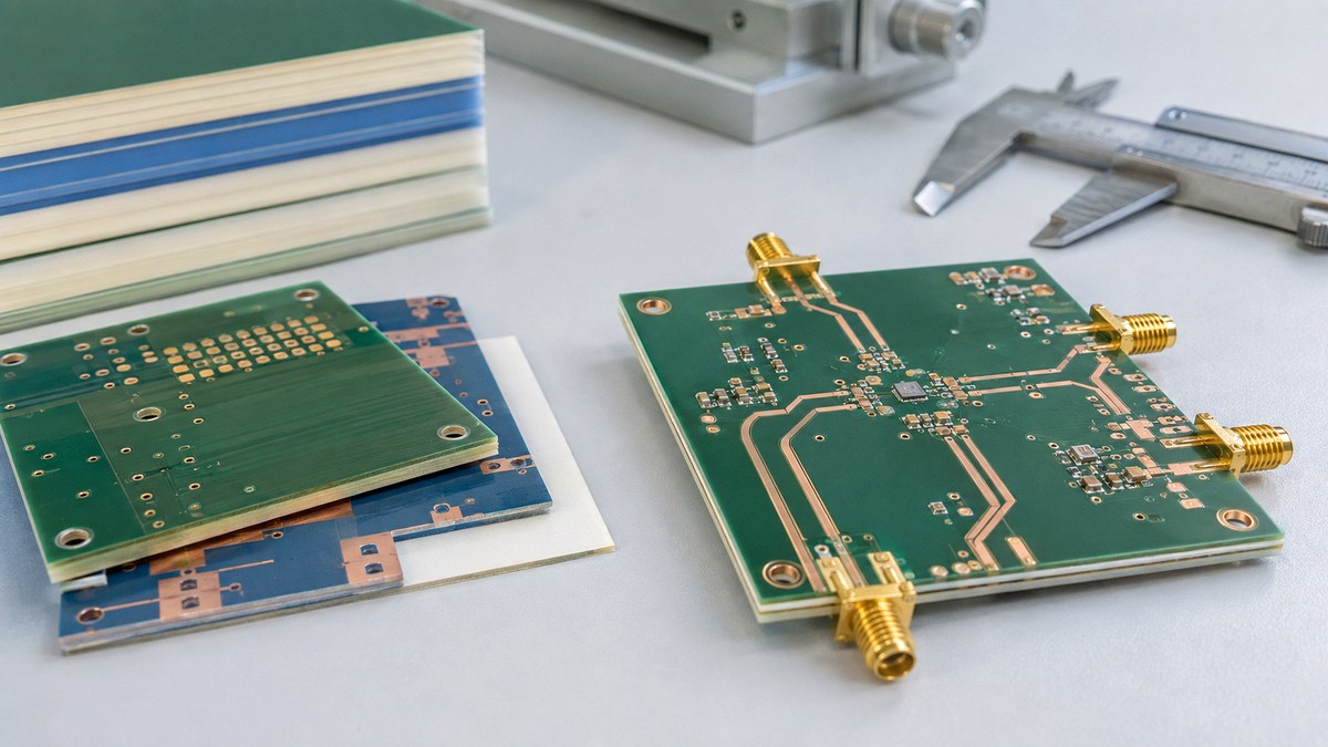
Case Studies: FR4 Signal Transmission PCB Prototype to Mass Production

This is a representative FR-4 production-control scenario. It shows the decisions and records needed from prototype release through repeat production.

Project background: A multilayer FR-4 signal transmission PCB carries differential links, clocks, and mixed-signal interfaces through board-edge connectors. Prototype assembly precedes production release.

Project requirements: The release package identifies controlled nets, impedance targets and tolerances, layer references, component models, maximum pair skew, connector launches, prototype quantity, assembly data, and requested impedance evidence. It also states which material substitutions require approval.

Engineering review: The fabricator checks whether the proposed dielectric thickness and finished copper produce manufacturable widths and gaps. The review flags traces crossing reference voids, layer transitions without nearby return vias, excessive unused via stub, ambiguous solder-mask conditions, and test coupons that do not represent the routed structures.

Prototype controls: The approved stackup, geometry, material rules, coupon design, drill options, assembly drawings, and test procedure form one controlled package. Inspection separates bare-board evidence from assembly and functional results.

Production transfer: Approved revisions, material identity, coupon results, inspection records, and accepted deviations form the production baseline. Review laminate, copper, stackup, drill, component, stencil, or test changes before use.

Customer-verifiable outputs: Specify the approved stackup, resolved engineering questions, material record, electrical test status, impedance report, inspection results, assembly records, and functional data in the purchase specification.

Why Choose Us for Controlled-Impedance PCB Prototyping and Assembly?

Choose a supplier by the risk it removes from your project. EBest Circuit combines experience since 2006 with design, prototyping, sourcing, assembly, and mass-production support. Signal transmission PCB customers can reduce supplier handoffs while keeping technical approvals and acceptance evidence visible.

  • Fewer engineering handoffs: One supplier can coordinate PCB design, prototype fabrication, component sourcing, assembly, and production transfer. This reduces revision mismatches between separate design, board, and assembly vendors.
  • Relevant board technologies: FR-4, multilayer, high-speed, high-frequency, impedance-control, HDI, high-Tg, flexible, and rigid-flex options support different channel, density, thermal, and mechanical requirements.
  • Prototype-to-production continuity: The approved stackup, engineering answers, coupon structures, inspection criteria, and accepted deviations can remain linked to the production revision. This lowers the risk of repeating an obsolete prototype decision.
  • Quality evidence matched to the risk: Buyers can specify electrical testing, TDR reports, AOI, X-ray, programming, or functional testing instead of relying on a general quality claim.
  • Support for regulated purchasing: EBest Circuit lists ISO 9001:2015, IATF 16949, ISO 13485:2016, AS9100D, UL, RoHS, and REACH support. Customers should confirm the current certificate or document, covered site, scope, and revision required for their order.
  • Controlled changes after approval: Material, copper, stackup, geometry, drilling, components, stencil, or test changes can be reviewed before use. This protects signal-integrity assumptions and avoids unapproved substitutions.
  • Practical urgent-build planning: Expedited options can be evaluated against material availability, quantity, assembly scope, testing, and shipping needs. Customers receive a project-specific commitment instead of an unsupported universal lead time.

Customer validation remains essential. Supplier records confirm conformance to released manufacturing requirements; they do not replace system simulation, protocol compliance, environmental qualification, or final product validation.

What Files and Specifications Are Required for a Signal Transmission PCB Quote?

A useful quote needs board, assembly, and test data. A complete signal transmission PCB quotation must identify the physical board, controlled structures, assembly scope, and verification plan. Missing stackup, impedance, or test information can produce a price that does not represent the intended build.

  1. Gerber or ODB++: Include every copper, solder-mask, legend, paste, profile, and mechanical layer with unambiguous layer names. This prevents missing layers, polarity errors, and artwork misinterpretation.
  2. NC drill files: Separate plated and non-plated holes and define slots, blind or buried vias, controlled-depth drilling, and backdrilling. This prevents the wrong via structure, residual stub, or mechanical mismatch.
  3. PCB stackup: State the layer order, finished copper, cores, prepregs, target dielectric thickness, material family, and permitted substitutions. These inputs are required for a valid impedance calculation.
  4. Controlled-impedance table: Identify each net class, single-ended or differential target, tolerance, routing layer, reference layer, mask condition, and coupon requirement.
  5. Fabrication drawing: Define board dimensions, finished thickness, copper, surface finish, solder mask, legend, profile, IPC revision and class, and special acceptance criteria.
  6. BOM and approved sources: Provide manufacturer part numbers, quantities, approved alternates, do-not-substitute parts, and sourcing responsibility. Highlight termination components and connectors that affect channel behavior.
  7. Centroid and assembly drawing: Include reference designators, X/Y coordinates, rotation, board side, polarity, special placement, and manual-assembly instructions.
  8. Test specification: Define the method, fixtures, limits, software, sample plan, calibration, report format, and customer-supplied test assets. State whether TDR, programming, functional testing, or interface validation is required.
  9. Commercial requirements: State prototype and production quantities, panel preference, delivery destination, packaging, revision, and requested schedule. This allows comparable pricing and lead-time review.
  10. Release status: Mark the package as design review or production release, list open decisions, and name the approval authority. This prevents unfinished data from being treated as approved production files.

Mark unfinished layouts as design-review releases and list open decisions. Do not treat a quote based on provisional impedance or material assumptions as production approval.

FAQs About Signal Transmission PCB

Q1: What impedance values are common on a signal transmission PCB?

A1: The interface specification and component guidance determine the required impedance. Single-ended and differential targets vary by protocol, connector, topology, and measurement reference. Do not copy a familiar value into the fabrication notes without identifying the controlled nets, tolerance, layers, and reference planes.

Q2: How should a signal transmission PCB impedance coupon represent production traces?

A2: The coupon should reproduce the controlled structure being accepted. Match the production layer, reference plane, dielectric construction, copper condition, mask condition, and relevant geometry. The drawing should identify which coupon trace corresponds to each impedance class.

Q3: What controlled-impedance tolerance should be specified?

A3: Set the tolerance from interface margin and measurement capability. A tighter number is not automatically better. Confirm whether the limit applies to nominal calculations, production coupons, or routed structures, and define the measurement method before ordering.

Q4: Why do PCB impedance calculators produce different results?

A4: They may use different equations, field solvers, material inputs, and geometry assumptions. Compare design Dk, pressed dielectric height, finished copper, plating, etched shape, solder mask, and frequency. Use the fabricator-approved stackup and correlate critical structures with a representative coupon.

Q5: Can a four-layer signal transmission PCB support controlled impedance?

A5: Yes, when the stackup provides a continuous nearby reference and producible geometry. Confirm dielectric height, finished copper, trace width, pair gap, plane continuity, and transitions with the fabricator. Layer count alone does not determine signal-integrity performance.

Q6: Why can prototype and production impedance results differ?

A6: Material, dielectric thickness, copper, etch, plating, resin flow, coupon design, and measurement setup can vary. Use the same approved construction, documented process controls, representative coupons, and change-approval rules to improve correlation.

Q7: Does length matching guarantee differential-pair signal integrity?

A7: No, length matching controls skew but does not correct impedance, loss, or return-path defects. The pair also needs symmetrical pads and vias, continuous reference planes, controlled coupling, suitable launches, and acceptable insertion and return loss.

Q8: Can a high-speed signal use a power plane as its reference?

A8: It can in a defined structure, but a continuous ground reference is usually easier to control. The power plane must remain continuous and provide a low-impedance high-frequency return relationship. If the reference changes, add an appropriate nearby return connection and validate the transition.

Q9: Does grounded copper beside a controlled trace change its impedance?

A9: Yes, nearby grounded copper can create coplanar coupling and shift the finished impedance. Define the copper gap, via stitching, mask condition, and keep-out in the field-solver model. Avoid uncontrolled or floating copper beside sensitive traces.

Q10: What should be checked after the fabricator changes trace width or pair spacing?

A10: Recheck more than the target impedance before approving the change. Verify clearance, differential coupling, delay, pair skew, pad neck-downs, solder mask, adjacent copper, routing density, and coupon geometry against the released stackup.

Conclusion

Reliability depends on preserving one controlled channel. A signal transmission PCB production release must preserve the approved stackup, geometry, return paths, transitions, assembly data, and acceptance evidence.

For a signal transmission PCB design review, controlled-impedance prototype, bare-board fabrication, PCB assembly, or production quotation, contact EBest Circuit at sales@bestpcbs.com. Send the Gerber or ODB++, NC drill, stackup, and impedance table. Include the fabrication drawing, quantity, BOM, centroid file, assembly drawing, and test requirements for engineering review before quotation.
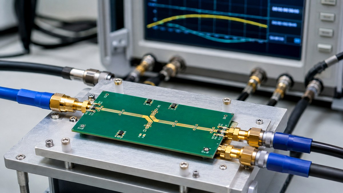
You may also like

Circuit Opening in PCB: Causes, Testing and Prevention

July 29th, 2026

Circuit opening in a PCB means that a conductive path intended to carry power or a signal has been interrupted. The affected branch carries no useful current, although voltage may remain on the source side of the break. On a bare board, the fault may be a broken trace, via-barrel discontinuity or missing inner-layer connection. On an assembled board, it may be an unsoldered terminal, lifted lead, cracked joint or failed component.

Circuit opening in PCB inspection and troubleshooting

What Does Circuit Opening Mean in a PCB?

In PCB work, circuit opening describes a loss of electrical continuity between points that should belong to the same net. The phrase is commonly used for an open circuit, open connection or open-net defect. It should not be confused with an intentionally open switch: both stop current, but only the unintended condition is a manufacturing or reliability fault.

The physical break can be obvious, such as a severed surface trace, or hidden inside a plated through-hole, multilayer interconnect, package termination or solder joint. A net may also behave as open only under heat, vibration or board flex. That intermittent condition can pass a room-temperature bench check and fail later in operation.

What Electrical Changes Occur When a Circuit Opens?

An ideal open circuit has zero current and infinite resistance. A real fault usually has resistance beyond the instrument range or a contact that changes between very high and lower resistance. The voltage behavior depends on where the break occurs and how the circuit is referenced.

  • Current: useful branch current falls to zero because the loop is incomplete.
  • Resistance: a powered-off continuity or resistance test normally shows OL or no beep across a complete break.
  • Voltage: source voltage can appear across an energized break, so an open circuit is not automatically safe to touch.
  • Signal state: a disconnected input may float, be forced by a pull-up or pull-down, or show coupled noise.
  • AC and high-frequency behavior: parasitic capacitance can pass a small displacement current even though DC continuity is absent.

A high-impedance voltmeter can therefore display voltage at an open node. That reading does not prove the path can deliver current; the voltage may collapse when a defined load is connected.

What Does an Open Circuit Diagram Show?

An open circuit diagram shows a gap in the intended current loop. In a simple source-switch-load circuit, opening the switch separates the contacts, sets branch current to zero and places most of the source voltage across the gap. For a PCB fault diagram, the gap should be marked on the specific net rather than drawn as a generic disconnected wire.

A useful diagnostic drawing includes the source, return path, expected load, test points and the suspected break. Net names and reference designators make it possible to transfer the diagram to the actual board without guessing which conductor belongs to the failed function.
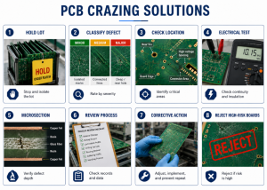
What Causes Circuit Opening in Bare PCB Fabrication?

Bare-board opens originate when the designed copper connection is missing, too thin, fractured or not joined between layers. The defect mechanism can usually be narrowed by its geometry and repetition pattern.

Bare PCB and assembled PCB circuit opening causes
  • Imaging or resist defects: missing artwork, debris, resist damage or poor development can remove part of a conductor.
  • Excessive local etching: a narrow trace can be necked down or fully separated. The related PCB etching process must be checked against artwork, copper weight and panel position.

  • Via or plated-hole discontinuity: drilling damage, desmear problems, poor activation, plating voids or barrel cracks can interrupt an interlayer path.
  • Inner-layer registration or lamination damage: a pad-to-hole connection may be lost, or an inner conductor may crack during processing.
  • Handling and routing damage: scratches, depaneling stress or edge breakout can sever traces after imaging and plating are complete.

If the same feature fails on every panel, data or tooling should be reviewed first. If failures repeat at one conveyor or panel position, imaging, spray, plating or handling equipment is more likely. Random isolated opens need microscopy and cross-section evidence before the process is adjusted.

What Causes Open Circuits During PCB Assembly?

Assembly opens occur when a valid bare-board net is not electrically joined through the installed component or connector. The failure may be visible, hidden beneath a package or mechanically intermittent.

  • Insufficient or missing solder paste caused by a blocked aperture, poor print alignment or unsuitable stencil design.
  • Non-wetting, poor flux activation or an unsuitable reflow profile that leaves the terminal electrically isolated.
  • Tombstoning, lifted leads or package warpage that separates one terminal during reflow.
  • Cracked solder joints, component terminations or PCB pads after thermal cycling, impact, vibration or excessive board strain.
  • Connector pins that are recessed, bent, contaminated or not fully seated.
  • Missing, damaged or internally open components, including fuses and inductors.

For BGA and QFN packages, an open must not automatically be described as a solder void. Non-wetting, head-in-pillow, pad cratering, package warpage and interconnect cracking require different evidence and corrective action.
Which Symptoms Indicate Circuit Opening?

Circuit opening symptoms depend on the affected net. A power-path open can disable the whole board, while a signal-path open may affect only one channel, sensor, communication line or output.

  • No power at a downstream rail even though the source voltage is present.
  • A missing clock, control or data signal after a specific component or connector.
  • An input stuck high, stuck low or unstable because its intended driver is disconnected.
  • A function that returns when the board, cable or connector is pressed or flexed.
  • Failure only during warm-up, cooling, vibration or high-current operation.

  • A continuity reading that changes when a joint or package is mechanically stressed.
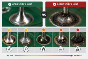
These symptoms identify the affected function, not the physical root cause. The schematic, netlist and board layout are needed to convert the symptom into a controlled test path.

How Do You Find an Open Circuit on a PCB?

Start from the failed function and trace one net at a time. Random probing can miss parallel paths or damage sensitive nodes.

  1. Review the schematic, net names, connector pinout and expected power sequence.
  2. Remove power and discharge stored energy before using continuity or resistance mode.
  3. Inspect connectors, fuses, component leads, test pads, vias and high-strain board areas under magnification.
  4. Check continuity between known endpoints, then divide a long path into smaller sections using accessible test points.
  5. If continuity is present but the function still fails, apply power safely and compare voltage or waveform measurements before and after each section.
  6. Use package-specific inspection when the suspected connection is hidden.

In-circuit readings can be affected by parallel components, protection devices and semiconductor junctions. A no-beep result is useful only when the expected path and meter threshold are understood.

How Should Continuity and Voltage Tests Be Used?

Continuity testing confirms whether a low-resistance path exists while the circuit is de-energized. Voltage testing shows how an energized circuit behaves. They answer different questions and should not be interchanged.

Continuity and voltage testing workflow for a PCB open circuit
Test Power State Useful Result Important Limit
Continuity Off Finds a complete low-resistance path Meter thresholds vary; parallel paths can beep
Resistance Off Shows OL, unstable contact or abnormal resistance Capacitors and semiconductors can change the reading
DC voltage On Shows where expected potential disappears An open node may still show phantom or unloaded voltage
Oscilloscope On Locates missing or distorted dynamic signals Probe reference and loading must be controlled

Never use resistance or continuity mode on an energized board. When voltage remains on both sides of a suspected open, compare the measurement under a known safe load and check whether the node is floating or capacitively coupled.

How Are Hidden and Intermittent Open Circuits Located?

Hidden opens require a test that matches the failure condition. A static room-temperature measurement cannot reliably expose a crack that opens only when materials expand or the board bends.

  • X-ray inspection: useful for package alignment, solder shape and some hidden joint anomalies, but not every planar crack is visible.
  • Cross-section analysis: confirms via-barrel, inner-layer, pad and solder-joint structure destructively.
  • Thermal stimulation: monitor continuity or function while temperature changes within controlled limits.
  • Mechanical stimulation: apply defined board flex or vibration while recording resistance; uncontrolled hand bending can create new damage.
  • Time-domain reflectometry: locates impedance discontinuities along long cables or transmission paths by distance.
  • Four-wire measurement: resolves small resistance changes in contacts and joints before a complete open develops.

Record temperature, load, fixture position and applied stress when the fault appears. Without repeatable conditions, an intermittent open may be reported as “no fault found” even when the defect remains.

How Do PCB Factories Detect Circuit Opening Defects?

No single inspection method covers every open. A manufacturing test flow combines image comparison, electrical continuity and functional evidence at the stage where each defect is detectable.

PCB factory detection flow for circuit opening defects
  • AOI: finds missing copper, neck-downs, solder defects and displaced components that are optically visible.
  • Bare-board electrical test: compares continuity and isolation against the approved netlist before assembly.
  • SPI and post-reflow AOI: screen paste deposition, placement and visible solder-joint conditions.
  • X-ray: examines hidden package and through-hole structures where optical access is limited.
  • ICT: checks nets, components and pin connections through a fixture and test program. The in-circuit testing guide explains its coverage and limitations.
  • FCT: verifies that the assembled board operates under defined inputs, loads and interfaces.

EBest Circuit (Best Technology) can support PCB fabrication and PCB assembly projects with process review and suitable inspection planning. The required test coverage should follow the design, access to test points, package types and reliability conditions rather than a generic test list.

What Is the Difference Between an Open, Closed and Short Circuit?

The three states differ by whether the intended path is complete and whether an unintended low-resistance path exists.

Condition Path Current Resistance Typical PCB Example
Open Intended path interrupted Zero in the affected branch Very high or unstable Cracked trace or unsoldered lead
Closed/normal Intended loop complete Defined by the load Expected circuit value Valid powered or signal connection
Short Unintended low-resistance path Potentially excessive Very low Solder bridge between nets

An open and a short can occur in the same assembly but require different localization methods. A short is found by identifying the unwanted connection; an open is found by identifying where the required connection disappears.

How Can Circuit Opening Defects Be Prevented?

Prevention requires controls at design, fabrication, assembly and verification stages. Testing alone can screen defects but cannot correct a weak design margin or unstable process.

  • Use conductor widths, annular rings, pad geometries and via structures compatible with the selected copper weight and fabrication process.
  • Protect neck-down traces and connections near board edges, slots, connectors and depaneling routes.
  • Balance stencil apertures, pad thermal mass and component orientation for stable solder paste transfer and reflow.
  • Control board support during assembly, connector insertion, screw fastening and test fixture contact.
  • Add accessible test points to critical rails, interfaces and long signal paths.
  • Match materials and joint design to thermal cycling, vibration and mechanical strain requirements.
  • Use fabrication AOI and netlist electrical testing before assembly, then apply assembly inspection and electrical tests appropriate to package visibility.

FAQ About Circuit Opening

What is another word for an open circuit?

Depending on context, engineers may use open connection, open net, discontinuity, broken circuit or circuit opening. On a PCB defect report, the net name and physical location are more useful than the general label alone.

How do you open a circuit intentionally?

A switch, relay, transistor in its off state, fuse or circuit breaker can intentionally interrupt a current path. The device rating must match the voltage, current, load type and switching transient.

Can current flow through an open circuit?

Ideal DC current is zero. In real circuits, leakage and parasitic capacitance may allow extremely small currents, especially at high frequency, but the path cannot carry its intended current.

Can an open circuit still have voltage?

Yes. Source voltage can appear across the break or at a floating node. Treat the circuit as energized until voltage is measured and the energy source is safely isolated.

What is the most common PCB circuit opening cause?

There is no universal single cause. Bare boards commonly involve conductor or via discontinuity; assembled boards commonly involve solder, terminal or mechanical connection failures. Failure location and repetition pattern should determine the investigation.

Conclusion

Circuit opening faults interrupt required power or signal paths, but the physical cause can originate in copper imaging, via plating, soldering, component contact or later mechanical and thermal stress. Reliable diagnosis starts with the schematic and netlist, separates powered and unpowered tests, and applies hidden-joint or intermittent-fault methods only where needed.

For PCB fabrication or PCBA support, contact EBest Circuit (Best Technology) at sales@bestpcbs.com.

You may also like