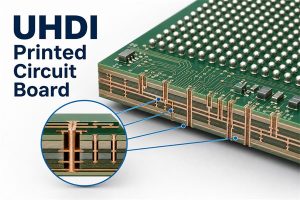
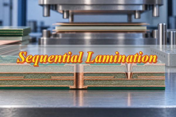
Sequential lamination builds a PCB in two or more controlled lamination stages so internal vias can be formed before later layers make them inaccessible. The practical question is not how many layers the board has. It is which blind, buried, or microvia connections must be completed at each stage and what those choices mean for reliability, cost, and lead time.
What Is Sequential Lamination in PCB?
A conventional multilayer PCB is usually bonded as one prepared stack. Sequential lamination pauses the build, forms connections in an accessible partial structure, adds another layer set, and continues outward.
A buried via can therefore be drilled and plated before later layers enclose it. Multi-level microvias follow the same logic: each lower tier is completed before the next dielectric covers its landing layer.
The deciding test is layer access. Trace every via from its drilling side to its target layer. If that connection can still be formed after the main bond, another build stage may be unnecessary. If the target becomes enclosed first, the stack must be divided into accessible substructures. Sequential lamination is therefore a construction sequence, not a performance grade.
How Is Sequential Lamination Different From Standard PCB Lamination?
The difference is when the internal connections are made. Standard construction completes most internal preparation before one main multilayer bonding stage. Sequential construction inserts drilling, plating, filling, or inspection between bonding stages.
| Factor | Standard Multilayer Lamination | Sequential Lamination |
|---|---|---|
| Lamination process | Mainly one multilayer bonding stage | Two or more controlled build stages |
| Via structures | Mainly through vias and structures accessible after bonding | Buried vias, blind vias, and multi-level microvias |
| Layer access | Internal layers become inaccessible after bonding | Selected layers remain accessible between stages |
| Process complexity | Lower when it meets the design | Higher because controlled operations repeat |
| Cost and lead time | Generally lower | Generally higher |
| Typical use | Conventional multilayer PCB | HDI and complex internal via structures |
A high layer count does not by itself require sequential lamination. A board with many layers and only plated through holes may use a conventional build, while a board with fewer layers but a buried via or several microvia tiers may need staged construction.
When Does a PCB Design Require Sequential Lamination?
Sequential lamination becomes necessary when a required connection cannot be drilled, plated, filled, or verified after the full stack has been bonded. Four design situations commonly create that condition:
- Buried vias that would be sealed inside the finished stack: the via must be completed in a core or sub-composite while both target layers are still exposed.
- Multiple HDI build-up layers: each added dielectric can create a new microvia level that must be formed before another layer is added.
- Stacked or multi-level microvias: the lower microvia usually needs controlled plating, filling, and a planar landing surface before the upper level is built.
- Fine-pitch BGA escape that cannot reasonably use through vias: adjacent-layer microvias can release routing area, but their start and stop layers determine the build sequence.
High layer count and the HDI label are not sufficient reasons by themselves. Hide the outer layers in the stackup view, add them back in build order, and note where a connection loses access before it is complete. That via map reveals whether staged construction is necessary and whether a routing change could remove a build-up tier.
How Does the Sequential Lamination Process Work?
The process follows the changing access to each via target. It starts with the innermost structure, adds a layer set, completes the connections that are accessible at that point, and repeats only when the stackup requires another tier.
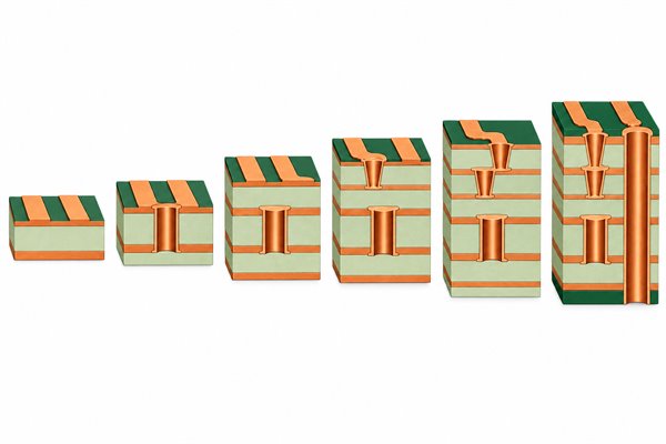
- Document the stackup and via spans. Identify every copper layer, dielectric, via start and stop layer, fill requirement, and controlled-impedance reference. The output is a build diagram that can be checked before routing is frozen.
- Build the initial core or sub-composite. Image and etch the inner copper, then align the partial structure. The layers that will support internal vias remain reachable.
- Drill and plate the internal vias. Form the buried holes or first accessible connections, then clean, metallize, fill, and inspect them as required. Their conductive path is complete before enclosure.
- Laminate the next layer pair or build-up layer. Add dielectric and copper to the verified partial structure. The result is a larger stack with a new outer surface available for processing.
- Form the next blind or microvia level. Drill and plate the newly accessible tier, using filling or planarization where another via must land above it. This completes the next connection level.
- Repeat as required and finish the PCB. Continue the add-layer-and-connect sequence for the remaining tiers, then complete final through holes, outer-layer processing, solder mask, finish, profiling, and the agreed testing.
This sequence explains the design consequence: adding or extending one via span can change the required build stages. It may add a fill dependency, alter which layer must remain exposed, or require another controlled cycle.
For the designer, the useful output is a confirmed build diagram: layer order, via levels completed at each stage, landing surfaces required by the next tier, and any geometry or material limit that changes the stackup.
How Do Different Via Structures Affect the Lamination Sequence?
Each via must be formed while its drilling side and target layer are accessible. The name of the via helps describe the connection, but the exact start-stop layers and stacking arrangement determine the sequence.
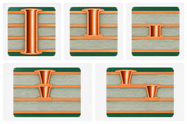
- Through vias: these normally pass through the completed stack and can be drilled after final lamination, so they do not create a sequential stage by themselves.
- Buried vias: these connect internal layers and must be processed before later layers hide both ends.
- Blind vias: these connect an outer surface to an internal target. Their route depends on the depth, dielectric thickness, drill method, and stage at which the target is exposed.
- Single-level microvias: these usually connect adjacent layers through a thin dielectric and may fit within one build-up stage.
- Stacked microvias: the upper microvia lands directly above the lower one, creating a fill and planarity dependency between tiers.
- Staggered microvias: the levels are offset, which avoids a direct via-on-via interface but does not necessarily remove the need to build each dielectric tier in sequence.
Do not assign a cycle count from terms such as blind via or HDI alone. Two boards can use the same via label yet require different sequences because the vias stop on different layers or use different fill and stacking arrangements.
How Does the PCB Stackup Determine the Number of Lamination Cycles?
The cycle count follows the number of connection groups that must be completed before another layer blocks access. Total layer count matters less than the order in which via targets disappear inside the stack.
Notation such as 1+N+1 or 2+N+2 shows the build-up layers around a core region, but it does not prove a universal press count. The core may contain buried vias, and outer tiers may be stacked, staggered, symmetric, or one-sided. The notation shows the layer arrangement; the via start-stop map shows the build dependencies.
Three simplified cases show how that logic changes the build:
- Eight-layer board with through vias only: the prepared layers can normally be bonded in the main multilayer lamination, followed by through-hole drilling. The layer count does not create another stage by itself.
- Core containing buried vias: the internal via is drilled and plated while its core or sub-composite is accessible. Outer layers are laminated only after that connection is complete, so the via architecture creates a staged build.
- 2+N+2 HDI with stacked microvias: the first microvia tier must be formed before the second build-up dielectric covers it. Direct stacking can also require a filled, planar lower via before the upper tier is added.
Estimate the sequence from the inside out:
- Map every start and stop layer. Separate through, blind, buried, and microvia spans.
- Group connections that are accessible together. Vias that can be formed in the same exposed sub-composite may share a stage.
- Mark each covering event. When a new dielectric hides a completed target, record the lamination needed before that happens.
- Add stacking dependencies. A microvia tier that needs a filled, planar lower via must be completed before the next tier can begin.
If two proposed builds show different cycle counts, compare their layer-by-layer diagrams, via formation stages, and fill sequence before treating either number as correct.
What Should You Check Before Finalizing a Sequential Lamination Stackup?
Review the stackup before dense routing makes the construction difficult to change. The goal is to prove that every added tier solves a real routing or electrical constraint and that its build dependency is understood.
- Via start and stop layers: make the CAD data, drill table, and cross-sectional stackup agree.
- Stacked or staggered arrangement: confirm whether direct stacking is necessary or an offset path can meet routing and reliability needs.
- Number of build-up tiers: test whether a routing change, another conventional layer, or a different escape pattern can remove a tier.
- Material system: check whether cores, prepregs, build-up dielectrics, and copper constructions suit the planned press and assembly thermal history.
- Impedance and reference layers: protect return paths, reference-plane continuity, dielectric targets, and any backdrill requirement when the build changes.
- Reliability requirements: state the product environment, assembly exposure, acceptance class, coupon needs, and qualification expectations.
Generic online limits should not be copied directly into CAD rules. Usable geometry depends on the material, dielectric thickness, copper, drill and fill process, registration capability, and product requirement. For a useful DFM or quotation review, send the stackup, via map, fabrication data, quantity, and reliability requirements together.
How Can Multiple Lamination Cycles Affect PCB Reliability?
Extra cycles add thermal, pressure, and registration exposure. That does not make a sequentially laminated PCB unreliable by definition, but it reduces the value of judging the design by layer count or a room-temperature electrical test alone.
| Risk area | Why multiple cycles matter | What to verify |
|---|---|---|
| Microvia interface | Repeated thermal exposure can reveal weak plating, fill, or target-pad interfaces | Via structure, fill route, representative coupons, and qualification method |
| Layer registration | Alignment error can accumulate as more structures are bonded | Capture pads, registration allowance, and evidence from intermediate stages |
| Material thermal history | The laminate experiences repeated heat and pressure before assembly reflow | Material suitability for the full fabrication and assembly history |
Risk is often concentrated at interfaces: a microvia base meeting its target pad, a filled via supporting an upper tier, or resin bonding around uneven copper. Residue, voids, weak plating, poor planarity, expansion mismatch, and registration error can reduce margin during reflow or thermal cycling.
Qualification should represent the connections with the greatest structural dependency. Match the coupon or test vehicle to the microvia tiers, target-pad interfaces, fill arrangement, materials, and expected assembly exposure. A room-temperature continuity check confirms a path at that moment; it does not reproduce repeated reflow or service thermal cycling.
How Does Sequential Lamination Affect PCB Cost and Lead Time?
Cost and lead time usually rise because pressing, drilling, plating, filling, planarization, and inspection may repeat for each build stage. There is no reliable universal percentage; the impact depends on the stackup, material, panel use, via density, registration demand, testing, and quantity.
- Repeated controlled operations: each added tier consumes equipment time and requires another alignment and processing sequence.
- Fill and planarization: stacked structures may need a prepared landing surface before the next level can be formed.
- Intermediate verification: hidden circuitry and via quality need to be checked before the next layer removes access.
- Longer dependency chain: later work cannot begin until the preceding structure is complete and suitable for the next tier.
- Greater late-stage loss: a defect found after several completed stages affects more accumulated processing than an early defect.
The best cost reduction is often one unnecessary build-up tier removed before layout release. Compare alternatives that preserve the same electrical and mechanical requirements, such as fewer unique via spans, staggered rather than stacked microvias, a different BGA escape, or an added conventional layer.
FAQs About Sequential Lamination Technology
Q1: What files help a supplier quote the actual build instead of making assumptions?
A1: Send one consistent data package. Include Gerber or ODB++ data, NC drill data, a controlled stackup, via start-stop layers, finished copper weights and board thickness, material and impedance requirements, via-fill or cap requirements, acceptance and test expectations, quantity, and target delivery date.
Q2: How should blind and buried via spans appear in the drill data?
A2: Every start-stop layer pair must be unambiguous. Separate drill files or a clearly mapped drill table can be used, but each span should identify its layer pair, plated status, finished size, tolerance, and any fill or cap requirement. The naming convention matters less than agreement between the drill data, stackup, and fabrication drawing.
Q3: Can stacked microvias be changed to staggered microvias without design approval?
A3: No. The alternative may improve the build margin, but it changes pad locations, routing space, and possibly reference-plane or impedance conditions. It should be proposed as a documented DFM change and approved in the controlled design data before production.
Q4: Why can two PCB quotations use different build sequences?
A4: The suppliers may be working from different assumptions or grouping operations differently. Compare the annotated build diagrams, via spans, fill and planarization route, materials, impedance construction, and test scope. A lower cycle number is not automatically the better or equivalent proposal.
Q5: Can an enclosed buried-via defect be repaired after final lamination?
A5: It is generally not a practical local rework. The connection is trapped inside the bonded stack, so opening it can damage surrounding layers and dielectric. Intermediate inspection, representative coupons, and final electrical testing are used to find problems; an affected bare board is usually rejected or rebuilt rather than patched.
Ready to build a sequential-lamination PCB? Send your stackup, Gerber or ODB++ files, via map, material and impedance requirements, quantity, and target delivery date to sales@bestpcbs.com. EBest Circuit can review the proposed construction and prepare a PCB quotation based on the actual build sequence.