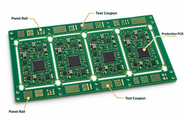
PCB test coupons are representative test structures placed on the same fabrication panel as the production boards. They are built with the same materials, copper plating, lamination, drilling, and other key processes so manufacturers can verify characteristics such as controlled impedance, plated-hole quality, via reliability, registration, and solderability without cutting into the finished PCB.
Different PCB test coupons serve different purposes. Impedance coupons are commonly checked with TDR, while structural coupons can be microsectioned to inspect plating and internal alignment. The coupon design should reflect the actual production stackup and fabrication process.

What Is a PCB Test Coupon?
A PCB test coupon is a dedicated test structure manufactured on the same panel as the production PCB to represent selected features of the finished board.
Unlike the functional PCB, the coupon is created specifically for inspection or measurement. Depending on the requirement, it may reproduce:
- Controlled-impedance traces
- Plated through holes
- Microvias or blind vias
- Internal layer registration features
- Copper plating structures
- Solderability features
The key point is representation. A useful coupon should experience the same relevant fabrication processes as the board it is intended to represent.
PCB test coupons are commonly placed in the panel rail or other non-product area, so testing does not consume a usable PCB.
At EBest Circuit, coupon requirements can be reviewed together with the production stackup during DFM. For controlled-impedance, HDI, RF, or high-reliability boards, this helps keep the test structure aligned with the actual PCB manufacturing conditions.
Why Are Test Coupons Used Instead of Testing the Production PCB?
PCB test coupons allow measurements and destructive inspections to be performed without damaging the production board.
Some verification methods cannot be carried out conveniently on a finished PCB. Microsection analysis, for example, requires the sample to be cut, mounted, polished, and inspected under magnification.
Coupons also provide a more consistent structure for tests such as TDR because production routing may contain:
- Vias
- Pads
- Connectors
- BGA breakouts
- Plane changes
- Short trace segments
These features can make measurement results harder to interpret.
A dedicated coupon can reproduce the required stackup and trace geometry while providing enough length and accessible test points for repeatable measurement.
The coupon therefore does not replace electrical or functional testing of the PCB. It provides process evidence for specific fabrication characteristics.
What Types of PCB Test Coupons Are Commonly Used?
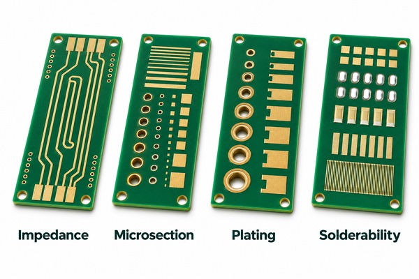
PCB test coupon types are usually selected according to what needs to be verified rather than by using one universal coupon design.
| Coupon / Test Structure | What It Checks | Typical Test Method |
|---|---|---|
| Impedance coupon | Single-ended or differential impedance | TDR |
| PTH structural coupon | Hole wall plating and registration | Microsection |
| Via reliability coupon | Via or interconnect integrity | Thermal stress / resistance monitoring |
| Microvia coupon | HDI microvia quality and stacking | Microsection / reliability test |
| Solderability coupon | Solder wetting performance | Solderability test |
| Peel-strength coupon | Copper adhesion | Peel test |
| SIR coupon | Surface insulation resistance | Electrical resistance testing |
Some IPC qualification and conformance structures use letter-based coupon designations. However, for most PCB buyers and engineers, the more useful question is not the letter itself but what manufacturing characteristic the coupon is intended to verify.
What Can PCB Test Coupons Verify?
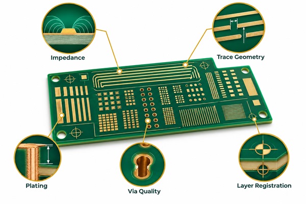
PCB test coupons can verify several manufacturing characteristics that are difficult to confirm from visual inspection alone.
Common checks include:
- Controlled impedance
- Copper plating thickness
- Plated through-hole integrity
- Microvia quality
- Annular ring condition
- Internal layer registration
- Solderability
- Copper adhesion
- Interconnect reliability
For example, an impedance coupon can confirm whether a nominal 50 Ω or 100 Ω structure is within tolerance after lamination, plating, and etching.
A microsection coupon serves a different purpose. It allows the manufacturer to inspect the actual cross-section of a plated hole or via and evaluate conditions such as copper distribution, registration, and interface quality.
Where Are Test Coupons Located on a PCB Panel?
PCB test coupons are usually placed in the panel rail or another non-functional area of the production panel.
This position allows the coupon to travel through the same major fabrication processes as the PCBs while remaining separate from the customer’s usable board outline.
A useful coupon should be positioned so that it represents the production process as closely as practical, especially for:
- Lamination
- Drilling
- Copper plating
- Etching
- Surface treatment
Coupon placement also needs to leave enough room for test access, sectioning, or removal from the panel.
For controlled-impedance production, the coupon is typically designed around the same layer pair, dielectric thickness, copper condition, and trace geometry used by the actual impedance-controlled routing.
How Are Impedance Test Coupons Tested with TDR?
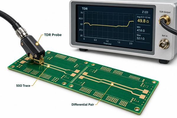
An impedance test coupon reproduces the controlled-impedance structure of the production PCB so its characteristic impedance can be measured with time-domain reflectometry, or TDR.
The coupon normally represents the same:
- Signal layer
- Reference plane
- Dielectric thickness
- Copper thickness
- Trace width
- Differential spacing, where applicable
- Material system
During TDR testing, a fast electrical edge is launched into the coupon. The instrument measures reflections along the transmission line and converts them into an impedance profile.
The result is then compared with the specified target, such as:
- 50 Ω single-ended
- 90 Ω differential
- 100 Ω differential
A typical tolerance may be ±10%, although tighter limits can be specified.
The coupon should be based on the final production stackup rather than only the original CAD trace width. Plating, etching, dielectric thickness, and manufacturing compensation can all change the finished impedance.
How Are Test Coupons Used for Microsection and Via Inspection?
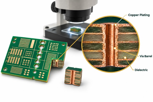
Microsection coupons are cut and polished so the internal PCB structure can be inspected directly under magnification.
This method is commonly used to evaluate plated through holes, blind vias, microvias, and multilayer registration.
A typical microsection can reveal:
- Hole-wall copper thickness
- Copper distribution
- Annular ring condition
- Layer-to-hole registration
- Resin condition
- Via interfaces
- Microvia geometry
- Lamination quality
Because the coupon is intentionally sacrificed, the production PCB remains intact.
For HDI boards, microsection inspection is especially useful because microvias, stacked structures, and thin dielectric layers can create manufacturing risks that are not visible from the board surface.
Microsection results should be interpreted against the relevant drawing, customer specification, and applicable IPC acceptance requirements rather than treated as a generic pass/fail image.
Who Should Design PCB Test Coupons—the Designer or the Fabricator?
PCB test coupon design is typically a shared responsibility: the PCB designer defines the electrical and reliability requirements, while the fabricator finalizes the coupon structure for the actual production process.
The customer should provide requirements such as:
- Target impedance
- Impedance tolerance
- Stackup constraints
- Material requirement
- Via structure
- Reliability requirement
- Required reports or inspection records
The fabricator then knows the actual production details, including dielectric availability, drill size, finished copper thickness, plating allowance, and etching compensation.
For that reason, it is often better for the PCB manufacturer to create or adjust the coupon after the production stackup is confirmed.
If a customer-supplied coupon is included in the fabrication data, it should still be reviewed during DFM to make sure it matches the manufacturing stackup and test method.

What Test Coupon Requirements Should You Include in Your PCB RFQ?
A PCB RFQ should clearly state what needs to be verified rather than simply asking for “test coupons.”
For controlled-impedance or high-reliability projects, provide:
- Gerber or ODB++ files
- PCB stackup or stackup constraints
- Material grade
- Finished board thickness
- Copper weight
- Target impedance
- Single-ended or differential requirement
- Impedance tolerance
- Critical routing layers
- Via or microvia structure
- Required test reports
- Whether physical coupons should be returned
For example, “50 Ω controlled impedance required” is less useful than specifying the routing layer, reference plane, stackup requirement, and tolerance.
FAQ About PCB Test Coupons
1. Is a PCB test coupon part of the finished PCB? No. It is normally placed in the panel rail or another non-product area and removed from the production panel.
2. Do I need to include a test coupon in my Gerber files? Not always. In many projects, the customer provides the test requirement and the PCB manufacturer creates the coupon based on the final production stackup.
3. What is an impedance test coupon? It is a representative transmission-line structure used to measure the finished PCB impedance, commonly with TDR.
4. Can a test coupon prove that every PCB on the panel is good? No. A coupon provides representative process evidence for specific characteristics. It does not replace board-level inspection or electrical testing.
5. Are PCB test coupons normally sent to the customer? They can be. Whether physical coupons, TDR reports, microsection images, or other records are supplied should be defined in the order or quality requirement.
6. What information should I provide for controlled-impedance coupon testing? Provide the target impedance, tolerance, routing layer, reference plane, stackup, material, copper weight, and any special coupon or reporting requirements.
Ready to Review Your PCB Test Coupon Requirements?
PCB test coupons are most useful when they are tied to a specific manufacturing risk, whether that is impedance, plating, microvia quality, registration, or another measurable characteristic. Defining the test requirement before production makes the coupon more representative and the resulting data more useful.
EBest Circuit supports controlled-impedance, HDI, RF, multilayer PCB manufacturing, PCBA, DFM review, TDR testing, and microsection inspection. For projects that require coupon-based verification, send your Gerber files and PCB specifications to sales@bestpcbs.com. Our engineering team can review the stackup, test requirements, and coupon approach before fabrication.
After coupon results are approved, our SMT assembly workflow can also coordinate circuit board stencil requirements with the released fabrication data.