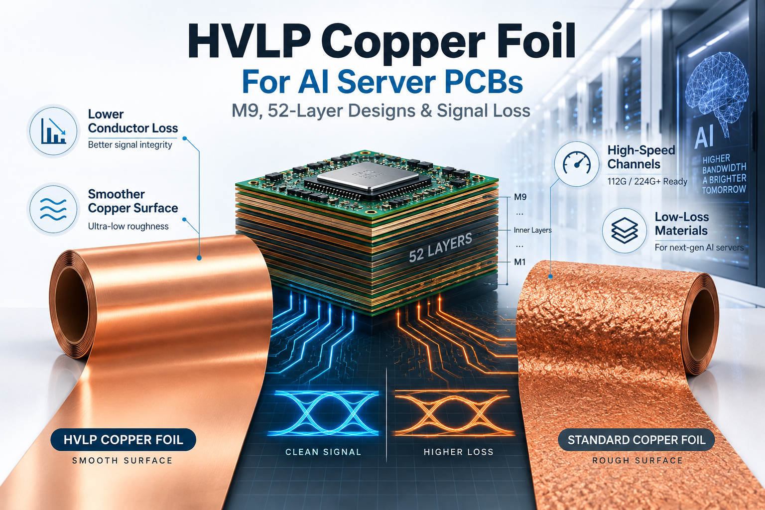
AI server PCB materials are entering another upgrade cycle. A September 16, 2026 industry report highlighted movement toward 52-layer PCB architectures and M9-class CCL as cloud providers continue expanding AI infrastructure. The change is not simply more copper layers; higher data rates are forcing designers to control dielectric loss, conductor loss, impedance consistency, and phase behavior together.
That is why HVLP copper foil is becoming more important. As resin and glass systems reduce dielectric loss, rough copper can consume a larger portion of the channel-loss budget. The practical question for PCB engineers is therefore no longer only “Which laminate grade should I use?” but also which copper profile is needed, on which layers, and how should that low roughness be preserved through fabrication?
Key Takeaways
- HVLP copper foil is used to reduce conductor loss in high-speed PCB channels by lowering the surface profile at the copper-dielectric interface.
- AI server PCBs are moving toward higher layer counts and lower-loss M9-class material systems, making copper roughness increasingly important alongside resin Df and glass construction.
- HVLP describes copper surface profile, not copper thickness. An 18 μm or 35 μm foil can still be a low-profile copper construction.
- A 52-layer PCB does not necessarily require HVLP on every layer. Long high-speed signal channels usually deserve the lowest-profile copper first.
- HVLP3, HVLP4, and HVLP5 are not universal IPC roughness classes. Engineers should verify actual Rz/Rq, foil thickness, treatment side, peel strength, and insertion-loss data.
- Very smooth copper creates a manufacturing trade-off: lower conductor loss must be balanced with sufficient copper-to-resin adhesion.
- PCB processing also matters. Aggressive inner-layer pretreatment can increase roughness and reduce the signal-integrity advantage of the incoming HVLP foil.
Why Is HVLP Copper Foil Demand Rising in AI Server PCBs?
HVLP copper foil demand is rising because AI server boards are combining more PCB layers with faster, longer loss-sensitive channels. The current AI infrastructure cycle is pushing higher-layer-count architectures together with M9-class material upgrades.
Three changes are happening at the same time:
- PCB layer counts are increasing.
- SerDes data rates continue moving toward 112G and 224G-class links.
- CCL systems are reducing dielectric loss, making conductor loss more visible.
The demand increase therefore comes from both more high-speed PCB material per server and a higher proportion of signal layers requiring smoother copper.
What Is HVLP Copper Foil?
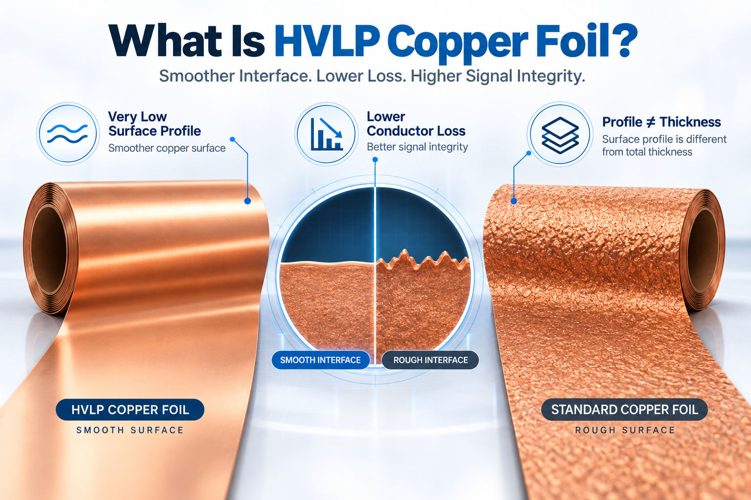
HVLP copper foil is a very-low-profile copper construction designed to maintain a smoother copper-dielectric interface than conventional electrodeposited copper.
The exact terminology varies by supplier. Some suppliers describe HVLP as ultra-low-profile copper, while the industry also uses “hyper very low profile” informally. What matters electrically is the actual surface morphology and measured roughness rather than the name alone.
Typical parameters to review include:
- Rz surface roughness
- Ra, Rq, or Sq where specified
- Treatment-side roughness
- Foil thickness
- Tensile strength
- Elongation
- Peel strength
Copper profile and copper thickness are different parameters. A smoother HVLP foil can still be supplied in common thicknesses such as 12, 18, or 35 μm.
HVLP vs VLP vs RTF vs Standard Copper Foil: What Changes?
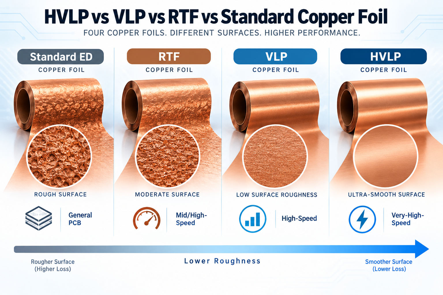
The main difference is the surface profile presented to the dielectric. Lower-profile foil reduces the microscopic path length seen by high-frequency surface current.
| Copper Foil Type | Surface Character | Typical Design Direction |
|---|---|---|
| Standard ED | Relatively rough | General-purpose PCB |
| RTF | Reduced profile on functional side | Mid- to high-speed PCB |
| VLP | Low profile | High-speed digital / RF |
| HVLP | Very low profile | Very-high-speed low-loss channels |
| Advanced HVLP | Extremely low profile | 112G/224G, AI server, mmWave-class applications |
These categories should not be treated as fixed global roughness ranges. Supplier processes, treatment methods, and naming conventions differ. For design work, the grade name should therefore be followed by the actual roughness specification and measured electrical performance.
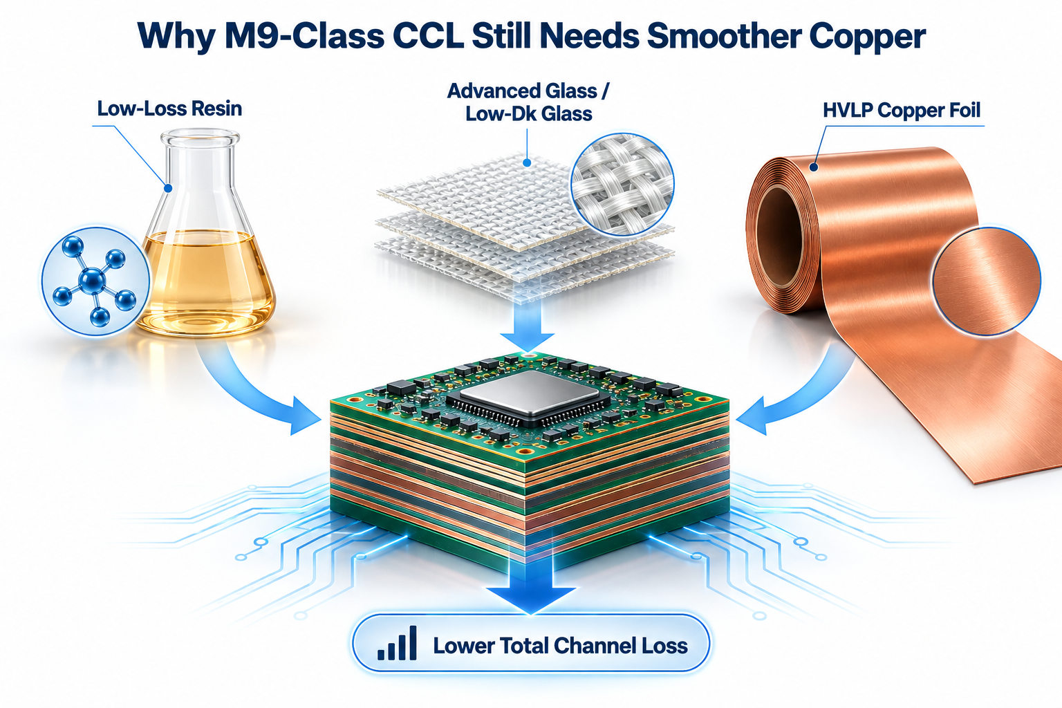
Why Does M9-Class CCL Still Need Smoother Copper Foil?
M9-class material reduces dielectric loss, but total channel loss also includes conductor loss. Improving only the resin and glass system does not eliminate loss caused by rough copper.
| Material Element | Main Role |
|---|---|
| Low-loss resin | Reduces dielectric loss |
| Low-Dk / advanced glass | Improves dielectric behavior and dimensional control |
| HVLP copper foil | Reduces conductor and insertion loss |
| Complete low-loss CCL | Balances all three for the required channel target |
At lower frequencies, dielectric loss may dominate enough that moderate copper roughness is acceptable. As signaling frequency rises, however, current becomes increasingly concentrated near the conductor surface.
That makes the microscopic copper profile part of the signal path. A very-low-Df resin paired with unnecessarily rough copper can therefore surrender part of the improvement gained from the dielectric system. M9 should be evaluated as a complete laminate system rather than as a resin grade alone.
How Does Copper Roughness Increase Conductor and Insertion Loss?
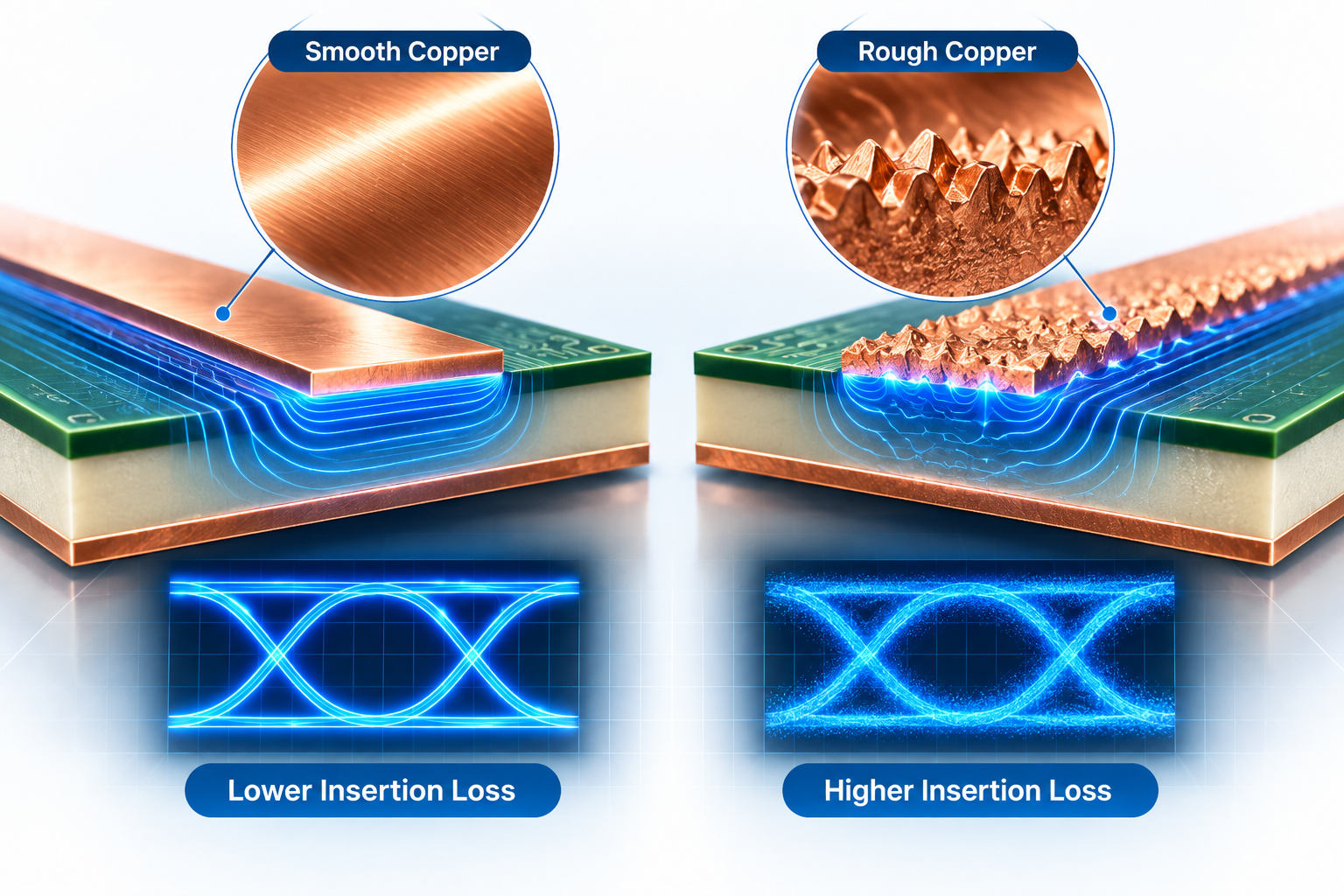
At high frequency, current flows primarily near the copper surface because of skin effect. When that surface is rough, the current follows a more complex microscopic path and experiences higher effective resistance.
The practical effects can include:
- Higher conductor loss
- Higher insertion loss
- Apparent changes in effective Dk
- Additional phase variation
- Greater channel-to-channel variation
Published test data has shown that copper profile alone can materially change insertion loss even when the dielectric material remains the same. The exact dB/in change depends on substrate, trace geometry, frequency, and foil construction, so loss figures should always be tied to the actual test vehicle.
Why Do 52-Layer AI Server PCBs Increase HVLP Copper Foil Demand?
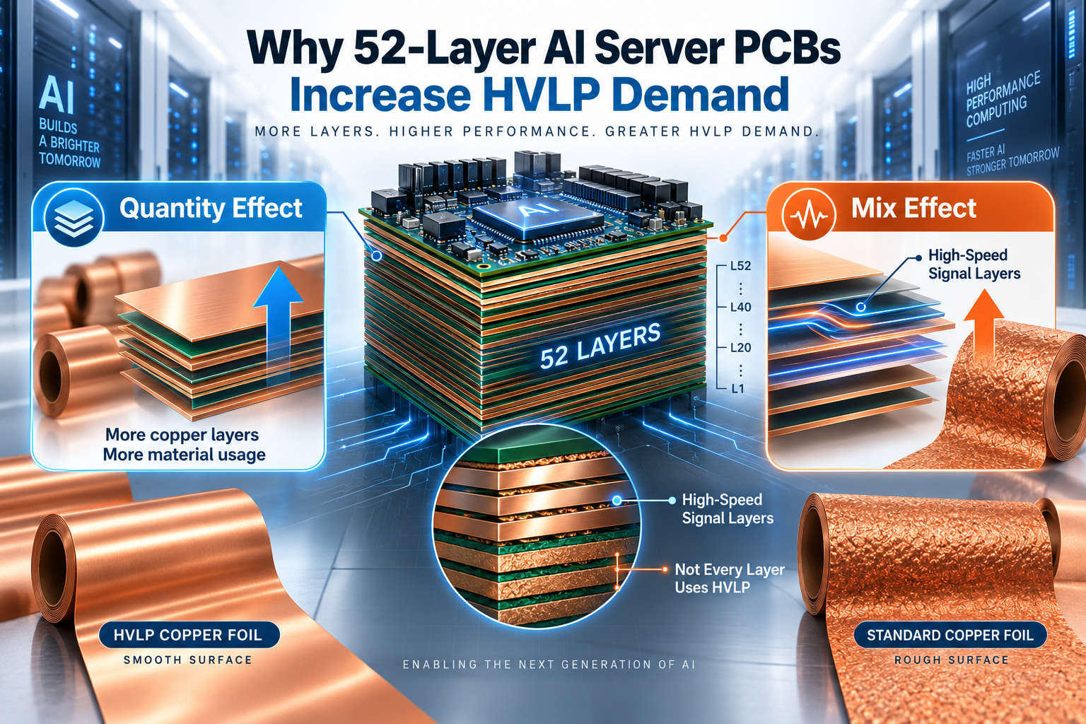
Higher layer counts increase HVLP demand through both a quantity effect and a material-mix effect.
Quantity effect
- More copper foil
- More CCL cores
- More prepreg
- More signal-layer area
- More lamination materials
Mix effect
At the same time, more routing may move from conventional foil or older low-profile grades toward lower-profile constructions as channel loss budgets tighten.
However, a 52-layer PCB does not mean all 52 layers use HVLP copper foil. Ground planes, power planes, short control traces, and lower-speed auxiliary layers may use different copper constructions.
Which PCB Layers Actually Need HVLP Copper Foil?
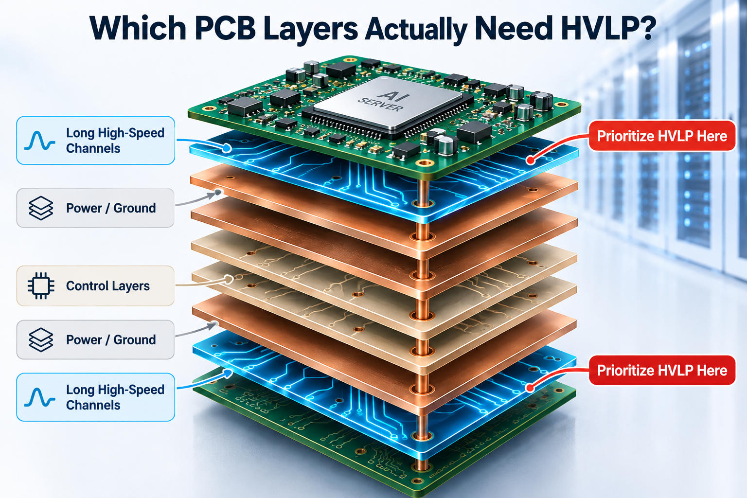
HVLP should normally be prioritized according to channel-loss sensitivity rather than applied to every copper layer by default.
Typical candidates include:
- Long SerDes routing
- 112G/224G-class channels
- PCIe and other high-speed differential links
- Switch and accelerator interconnects
- Backplane or midplane routing
- Loss-sensitive memory/network interfaces
- High-frequency RF or mmWave layers where applicable
Layers that may not require the same profile include:
- Power planes
- Ground planes
- Short GPIO routes
- Low-speed management buses
- Short local control connections
The actual choice depends on trace length, data rate, dielectric thickness, insertion-loss budget, and laminate system.
HVLP3 vs HVLP4 vs HVLP5: How Should Engineers Interpret the Grades?
HVLP3, HVLP4, and HVLP5 generally indicate progressively smoother copper within a supplier’s product family, but these labels are not universal IPC roughness classifications.
When comparing grades, engineers should request:
- Rz
- Ra / Rq / Sq where available
- Treatment-side roughness
- Copper thickness
- Treatment chemistry
- Peel strength
- Resin compatibility
- Insertion-loss test data
A buyer should therefore avoid specifying only “HVLP4 required.” A better requirement links the foil grade to a named laminate construction, roughness target, and electrical loss objective.
What Manufacturing Challenges Come with HVLP Copper Foil?
The manufacturing challenge with HVLP is to keep the copper surface smooth enough for low loss while maintaining enough adhesion to survive lamination, thermal cycling, and assembly.
Important controls include:
- Copper-to-resin bonding
- Inner-layer pretreatment
- Brown oxide or alternative oxide chemistry
- Lamination pressure and temperature
- Resin compatibility
- Etching compensation
- Peel strength
- Impedance consistency
- Layer registration
- High-layer-count warpage
PCB processing can change the incoming copper surface. The relevant question is not only “Was HVLP purchased?” but also “What roughness remains at the finished signal interface after fabrication?”
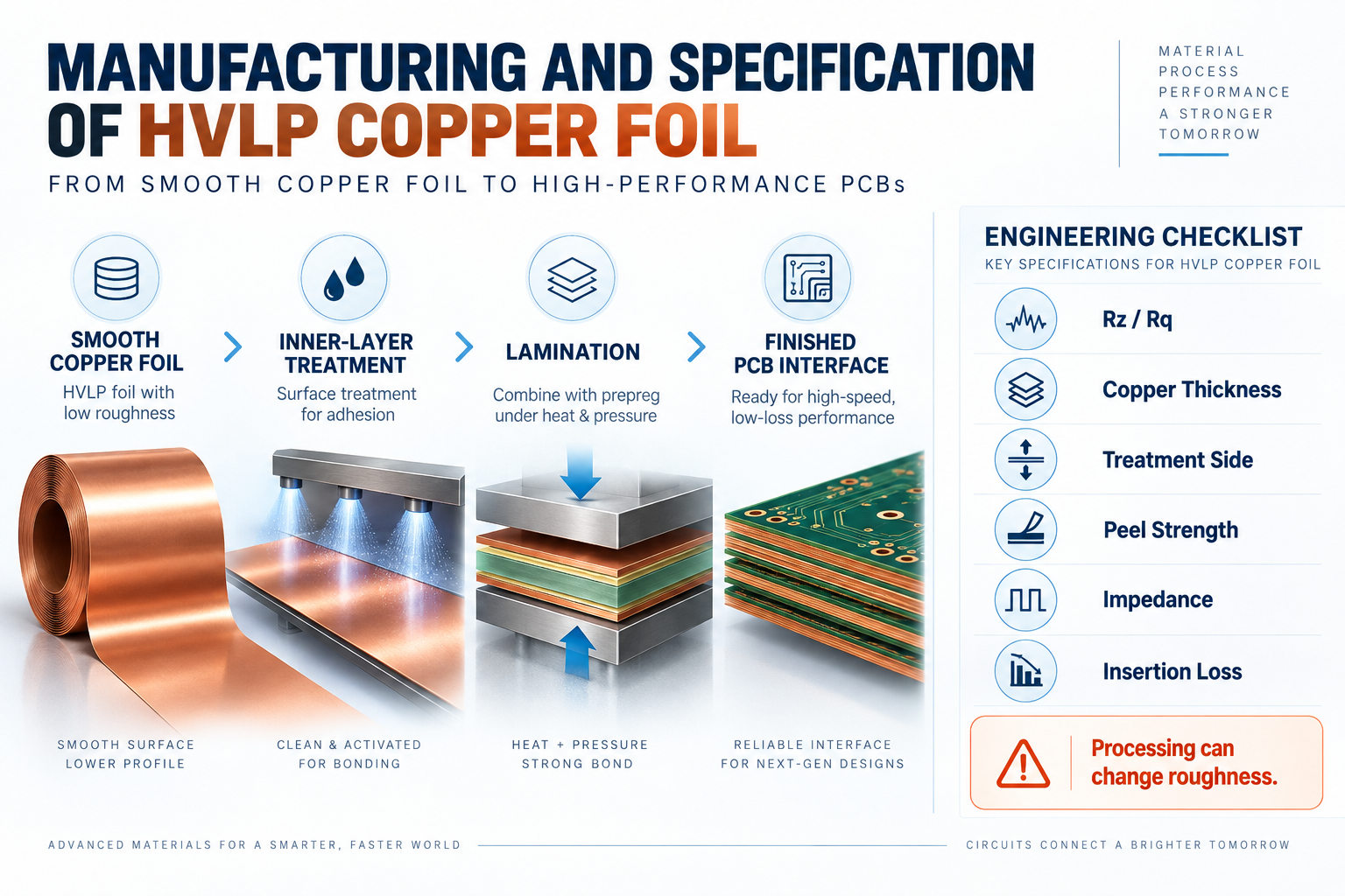
How Should Engineers Specify and Verify HVLP Copper Foil?
An HVLP requirement should connect the material specification to the actual electrical channel requirement.
For quotation or stackup review, provide:
- Target data rate
- Operating or Nyquist frequency
- PCB layer count
- Laminate family
- Copper foil supplier and grade, if mandatory
- Copper thickness
- Required Rz / Rq / Sq
- Treatment side
- Layers requiring HVLP
- Impedance tolerance
- Maximum insertion loss
- Critical trace length
- Peel-strength requirement
- Thermal and reliability requirements
Verification may include:
- Impedance coupons
- TDR
- Insertion-loss coupons
- VNA / S-parameter testing
- Material certificate or COC
- Lot traceability
For very-high-speed projects, the laminate, glass style, copper foil, stackup geometry, and fabrication treatment should be qualified together rather than approved as independent specifications.
What Cost and Supply Risks Should Buyers Check for HVLP4 and HVLP5?
Higher-grade HVLP introduces both material-cost and supply-chain risk because qualification is more restrictive than for standard copper foil.
When selecting an HVLP copper foil supplier, compare the actual Rz/Rq limits, treatment method, laminate qualification, and measured channel-loss data rather than relying on the grade name alone.
Buyers should check:
- Qualified copper-foil suppliers
- Qualified CCL combinations
- Minimum order quantities
- Lead time
- Alternative material approval
- Lot-to-lot roughness control
- Qualification quantities
- Insertion-loss validation
- Whether substitutions require customer approval
A lower-cost foil with the same “HVLP4” label should not automatically be treated as electrically or mechanically equivalent. The actual laminate system, surface treatment, roughness, adhesion, and measured channel loss still need qualification.
FAQ About HVLP Copper Foil
1. What does HVLP mean in copper foil?
HVLP refers to very-low-profile copper foil developed for lower conductor loss. Supplier terminology varies, so the actual Rz/Rq and product specification are more important than the acronym alone.
2. Is HVLP copper thinner than standard copper foil?
No. Copper thickness and copper surface profile are separate parameters. HVLP can be supplied in common foil thicknesses such as 12, 18, or 35 μm.
3. What is the difference between VLP and HVLP copper foil?
Both reduce copper surface roughness, but HVLP generally targets a lower surface profile and more demanding high-speed channels. Exact roughness limits depend on the supplier.
4. Does M9 CCL always use HVLP5 copper foil?
No. M9-class material systems vary by laminate supplier and application. The required copper profile depends on data rate, stackup, trace length, insertion-loss target, and qualified material construction.
5. Does every signal layer need HVLP copper foil?
No. HVLP is normally prioritized for the most loss-sensitive signal layers. Short low-speed routes and non-signal planes may use other copper constructions.
6. What roughness value should I specify for a high-speed PCB?
There is no universal Rz value for every high-speed design. The correct target should be derived from the channel-loss budget and verified against the actual foil, laminate, stackup, and fabrication process.
Planning a High-Speed PCB with HVLP Copper Foil?
HVLP selection is only one part of a high-speed material system. Laminate Dk/Df, glass style, copper profile, trace geometry, layer assignment, impedance, inner-layer treatment, and insertion-loss testing all need to work together.
EBest Circuit can review stackup requirements, impedance targets, copper thickness, laminate availability, HVLP requirements, and manufacturability before quotation. For advanced low-loss PCB projects, send your Gerber files, stackup, material requirement, target impedance, and loss specification to sales@bestpcbs.com for engineering review.