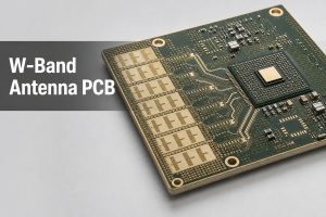
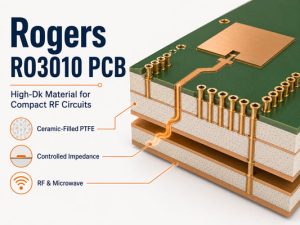
A PCB transmission line is a signal trace designed together with its reference plane and dielectric so that signals travel with controlled characteristic impedance. A trace should be treated as a transmission line when its propagation delay becomes significant compared with the signal rise or fall time.
Common PCB transmission line structures include microstrip, stripline, and coplanar waveguide. Their impedance depends on trace width, copper thickness, dielectric thickness, Dk, and reference-plane geometry. For controlled-impedance designs such as 50 Ω, the final stackup should be verified with the PCB manufacturer and tested by TDR after fabrication.
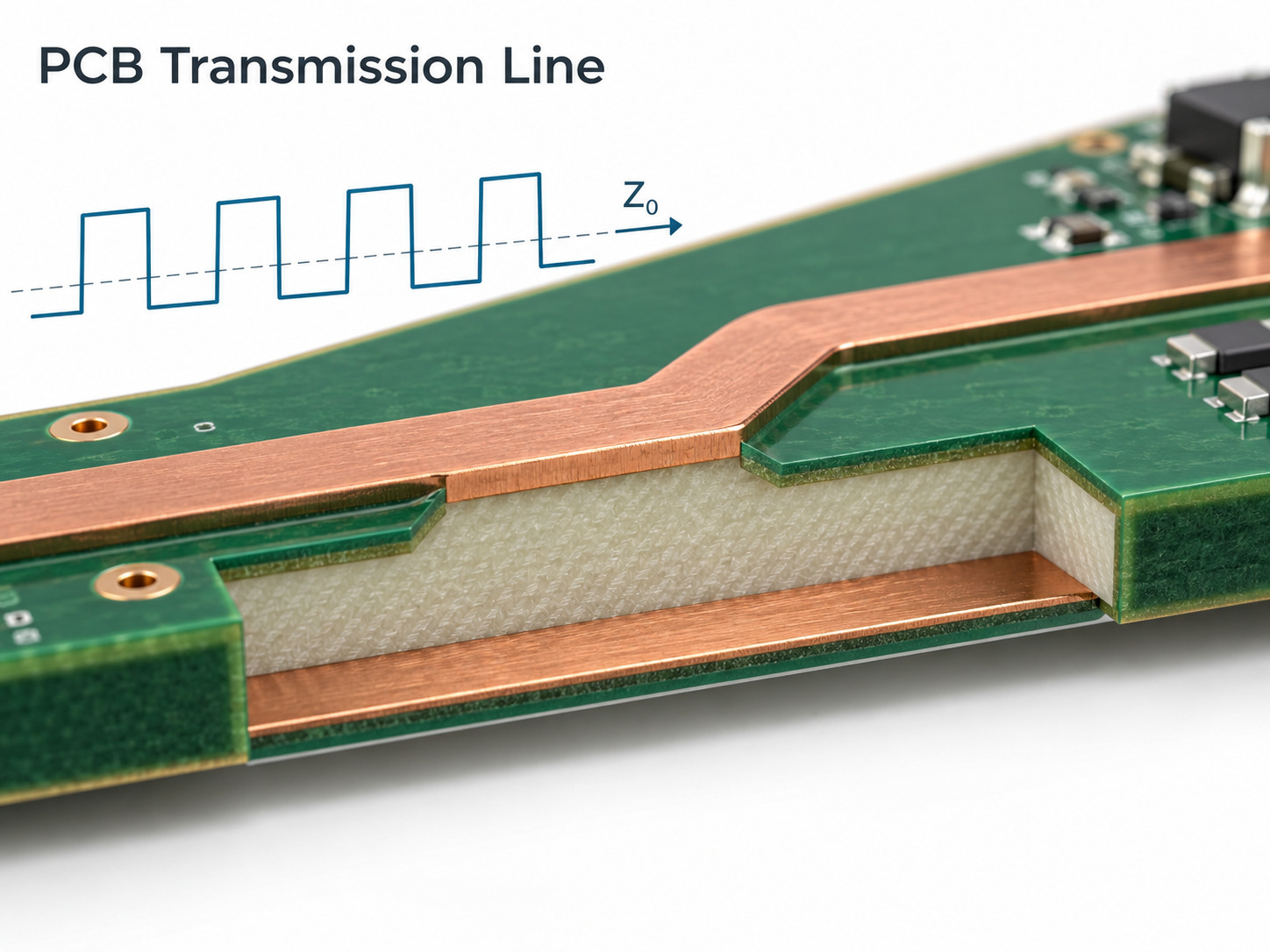
What Is a Transmission Line on a PCB?
A PCB transmission line is a signal conductor arranged with a defined reference path so that its impedance and signal propagation can be controlled.
It normally includes:
- A copper signal trace
- A continuous reference plane
- Dielectric material between signal and reference
- Defined trace width and copper thickness
- Controlled spacing to nearby copper
- A predictable return-current path
At low signal speeds, a short PCB trace can often be treated as a simple connection. As signal edges become faster, voltage and current no longer appear everywhere on the trace at the same instant. The signal travels along the interconnect as an electromagnetic wave.
This is why the transmission line is not just the visible copper trace. The reference plane and dielectric are also part of the structure.
When Does a PCB Trace Become a Transmission Line?
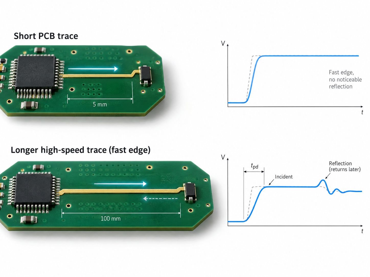
A PCB trace should be treated as a transmission line when its propagation delay becomes significant compared with the signal rise or fall time.
Clock frequency alone is not enough to make this decision. A relatively low-frequency signal with a fast edge can still experience reflection and impedance problems.
The main factors are:
- Signal rise and fall time
- Trace length
- Propagation delay
- PCB dielectric properties
On common FR-4 structures, propagation delay is often around 150–180 ps per inch, depending on the stackup and transmission line geometry.
A useful first-pass rule is to start treating the route as a transmission line when its one-way delay approaches roughly one-sixth of the signal rise time.
So the better design question is not simply “What is the clock frequency?” but “How long does the signal take to travel through the PCB interconnect compared with its edge time?”
What Are the Main PCB Transmission Line Types?
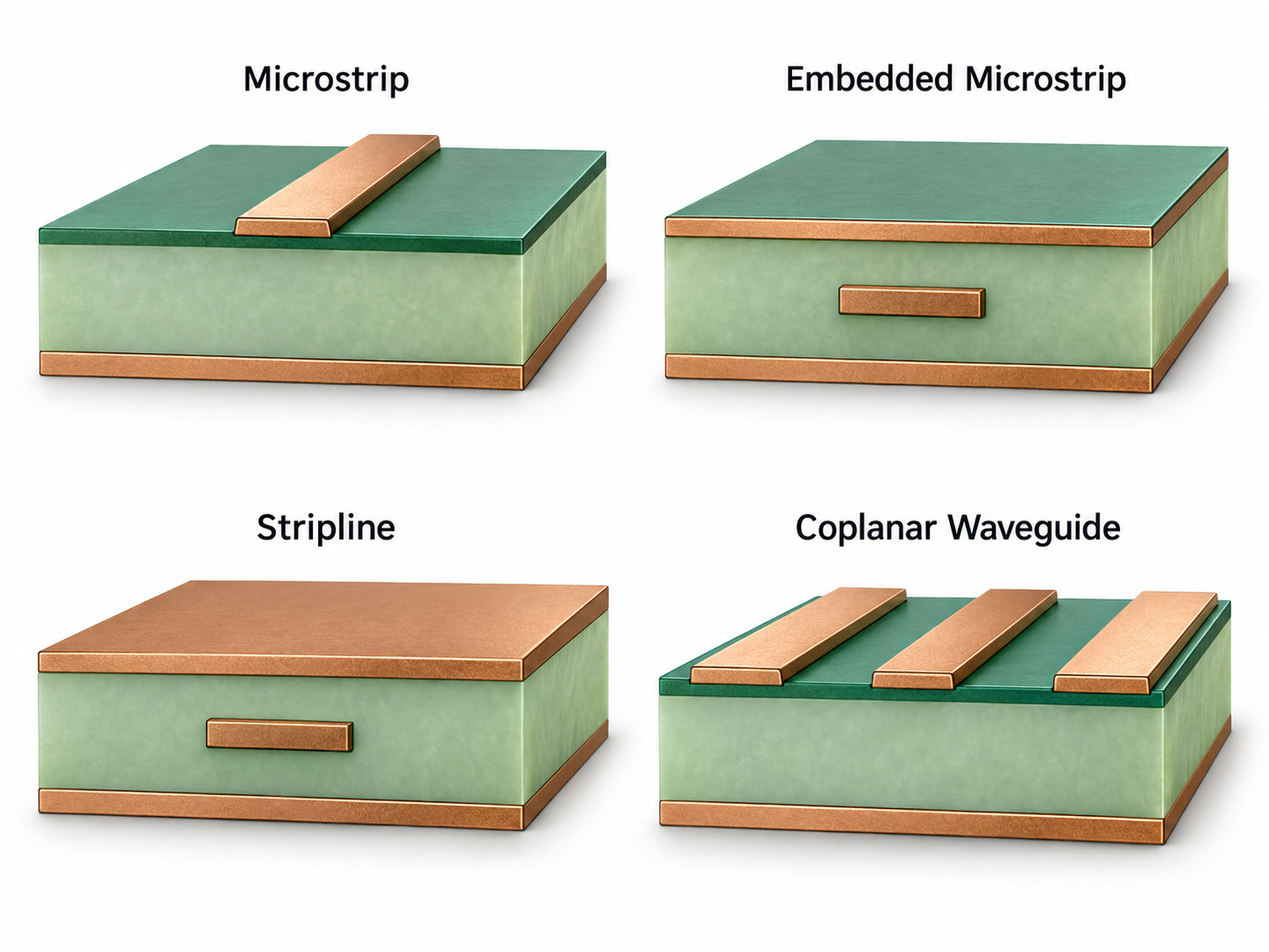
Common The main PCB transmission line types are microstrip, embedded microstrip, stripline, and coplanar waveguide. Their main difference is how the signal trace is positioned relative to the reference plane and nearby ground copper.
| Type | Structure | Common Use |
|---|---|---|
| Microstrip | Outer trace over a plane | RF and high-speed digital |
| Embedded microstrip | Trace covered by dielectric | Controlled outer-layer routing |
| Stripline | Inner trace between planes | High-speed internal routing |
| Coplanar waveguide | Signal with side ground copper | RF and microwave |
| Grounded coplanar waveguide | Side ground plus lower plane | RF and antenna routing |
Microstrip is convenient for surface-mounted components and RF connectors. Stripline provides stronger field confinement inside the PCB. Coplanar structures are often selected when RF routing needs tighter control around the signal trace.
At EBest Circuit, transmission-line review can be included during DFM and stackup evaluation before PCB fabrication. For projects that also require PCBA, the review can extend to connector transitions, BGA breakout, component placement, and assembly constraints so that the controlled-impedance structure remains practical after the bare PCB moves into assembly.
What Determines PCB Transmission Line Impedance?
PCB transmission line impedance is mainly controlled by trace geometry, dielectric properties, and the distance between the signal trace and its reference plane.
Important parameters include:
- Trace width
- Finished copper thickness
- Dielectric thickness
- Material Dk
- Reference-plane position
- Transmission line type
- Spacing to nearby copper
- Solder mask
For a typical microstrip, wider traces generally lower impedance, while greater distance to the reference plane tends to increase it.
This is why there is no universal trace width for 50 Ω. A 0.15 mm trace may be close to 50 Ω on one stackup but significantly different on another.
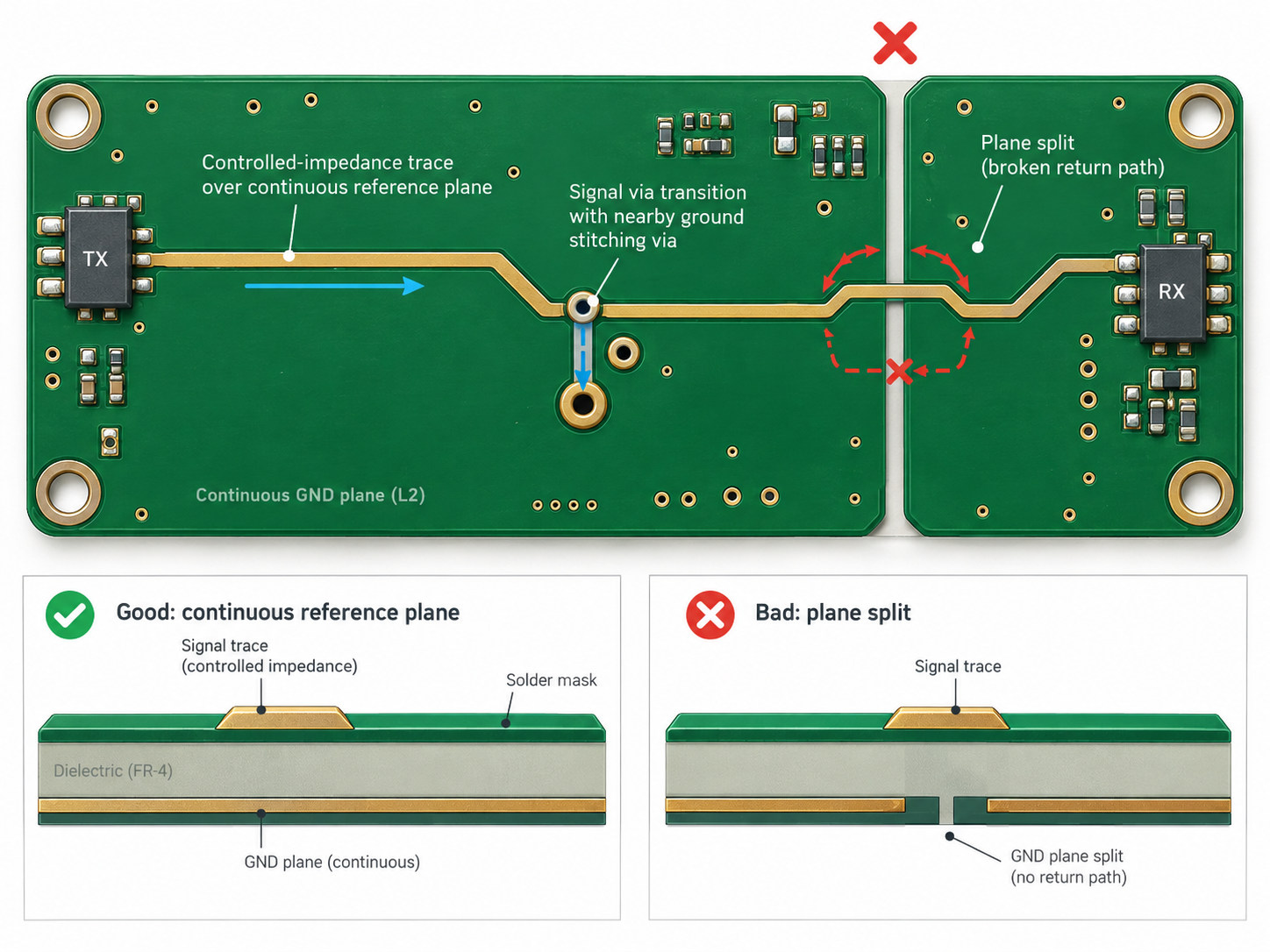
The reference plane must also remain continuous. Plane splits, large voids, and abrupt reference changes can disturb the electromagnetic field even when trace width remains unchanged.
How Do You Design a 50 Ohm Transmission Line on a PCB?
A 50 ohm PCB transmission line is designed by matching trace geometry to the actual PCB stackup until the calculated characteristic impedance reaches approximately 50 Ω.
The design should start with:
- Signal layer
- Reference plane
- Material type
- Dielectric thickness
- Finished copper thickness
- Target impedance
- Impedance tolerance
There is no fixed 50 Ω trace width that works for every PCB.
A practical design process is:
- Define the 50 Ω target.
- Confirm the PCB stackup.
- Select microstrip, stripline, or another structure.
- Calculate the initial trace dimensions.
- Verify the cross-section with a field solver.
- Apply manufacturing compensation if required.
- Fabricate an impedance coupon.
- Verify the finished result with TDR.
50 Ω is widely used because many RF cables, connectors, instruments, amplifiers, filters, and antennas are designed around the same impedance environment.
How Is PCB Transmission Line Impedance Calculated?
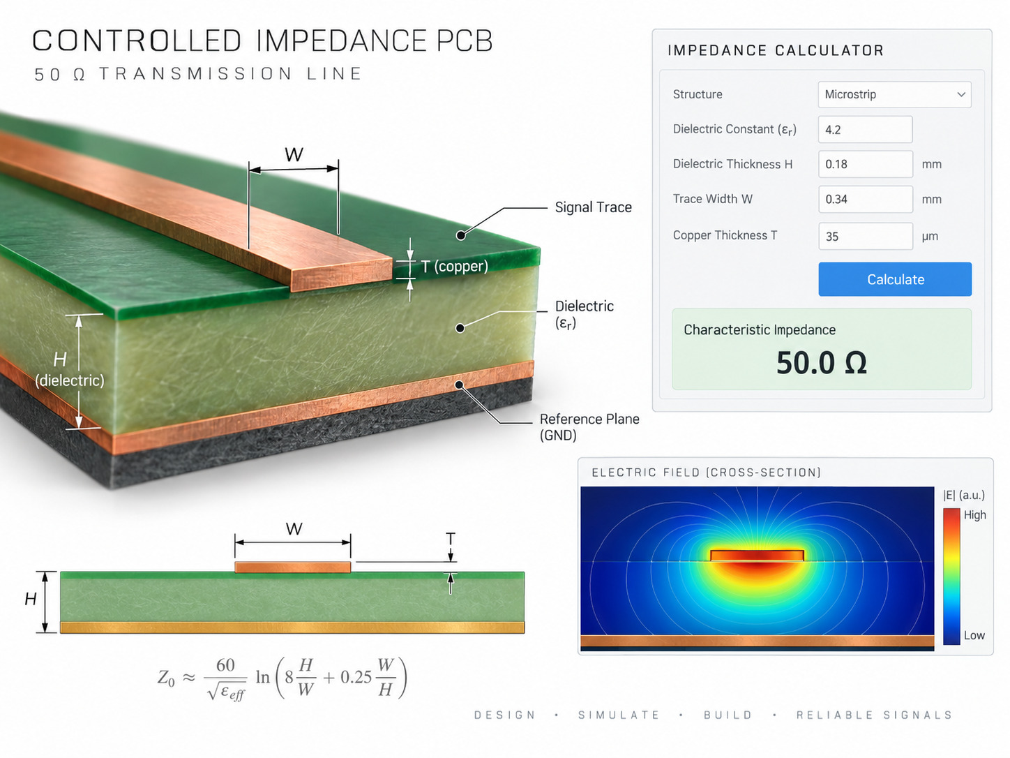
A PCB transmission line calculation can be estimated with analytical formulas, online calculators, or electromagnetic field solvers.
Analytical formulas are useful for understanding how trace width, dielectric thickness, copper thickness, and Dk affect impedance.
A PCB transmission line impedance calculator is useful for early estimates, but the result should be checked against the final production stackup.
Online PCB transmission line calculators are convenient for early layout. Typical inputs include:
- Trace width
- Copper thickness
- Dielectric thickness
- Dielectric constant
- Ground spacing
Different calculators may produce slightly different values because they use different equations and assumptions.
For final controlled-impedance production, a 2D field solver is usually more reliable because it can model the actual PCB cross-section, including conductor shape, dielectric regions, solder mask, and coplanar spacing.
What PCB Layout Rules Keep Transmission Line Impedance Stable?
Good PCB transmission line layout design keeps the routing geometry and return path consistent along the signal route.
Key layout rules include:
- Route over a continuous reference plane.
- Avoid unnecessary trace-width changes.
- Keep neck-down sections short.
- Minimize unnecessary vias.
- Provide a return path during layer changes.
- Control spacing to nearby traces and copper.
- Avoid long via stubs on very high-speed signals.
A signal via changes the local transmission structure, so its pad, antipad, barrel, and stub can affect high-speed performance.
Connectors, pads, vias, and package breakouts should also be treated as part of the channel. A well-controlled 50 Ω trace can still experience reflections if these transitions create large impedance discontinuities.
How Is PCB Transmission Line Impedance Controlled and Tested in Manufacturing?
PCB manufacturers control transmission line impedance by matching the electrical target to the actual production stackup, compensating the artwork when necessary, and verifying the finished structure with TDR.
Before fabrication, the manufacturer normally reviews:
- Material grade and Dk
- Dielectric thickness
- Finished copper thickness
- Trace width and spacing
- Target impedance
- Required tolerance
Production artwork may be adjusted slightly because plating and etching change the finished conductor geometry.
For controlled-impedance boards, an impedance coupon is usually fabricated on the same panel. TDR testing then checks whether the finished structure meets the specified impedance.
Common requirements include:
- 50 Ω ±10%
- 90 Ω differential ±10%
- 100 Ω differential ±10%
For quotation and stackup review, provide the Gerber or ODB++ files, material requirement, copper weight, target impedance, routing layer, and tolerance.

FAQ About PCB Transmission Lines
1. Is every PCB trace a transmission line? Technically yes, but transmission line analysis is normally needed only when trace delay becomes significant compared with the signal rise or fall time.
2. Why is 50 ohms commonly used for PCB transmission lines? Because many RF cables, connectors, instruments, antennas, and components are designed around a 50 Ω system.
3. What is the difference between microstrip and stripline? Microstrip runs on an outer PCB layer above a reference plane. Stripline runs inside the PCB between reference planes.
4. Does PCB trace length change characteristic impedance? No. Characteristic impedance is mainly determined by geometry and dielectric properties. Length mainly affects propagation delay, loss, and phase.
5. Can FR-4 be used for a 50 ohm transmission line? Yes. FR-4 is suitable for many 50 Ω designs, although lower-loss laminates may be preferable at higher frequencies or where insertion loss is tightly controlled.
6. How is PCB transmission line impedance measured? It is commonly verified with TDR using an impedance coupon fabricated with the production panel.
Ready to Review Your PCB Transmission Line Design?
A transmission line that calculates as 50 Ω may shift after the final dielectric thickness, copper plating, and etching process are defined. Reviewing the production stackup before fabrication helps reduce impedance deviation and avoid unnecessary revisions.
EBest Circuit supports controlled-impedance PCB manufacturing and PCBA for high-speed digital, RF, microwave, HDI, Rogers, hybrid-material, and low-loss multilayer projects. If you have similar projects, you are welcome to send your Gerber files and detailed PCB specifications to sales@bestpcbs.com for stackup and DFM review.