





PCB delamination is the loss of adhesion between layers or interfaces inside a printed circuit board. In a high-end multilayer PCB, the separation may occur between copper and resin, within the dielectric system, around glass reinforcement, or near a plated hole. It may remain hidden until lamination, lead-free assembly, rework, or field heating adds enough pressure and stress to open the weak interface.
Advanced material does not automatically mean a board is more likely to delaminate. The risk rises when low-loss resin systems, smoother copper, thin dielectrics, dense copper patterns, hybrid materials, repeated lamination cycles, and high-temperature assembly are combined without a matched process window. Preventing the defect requires control of the complete material-and-process system, not a single datasheet value.
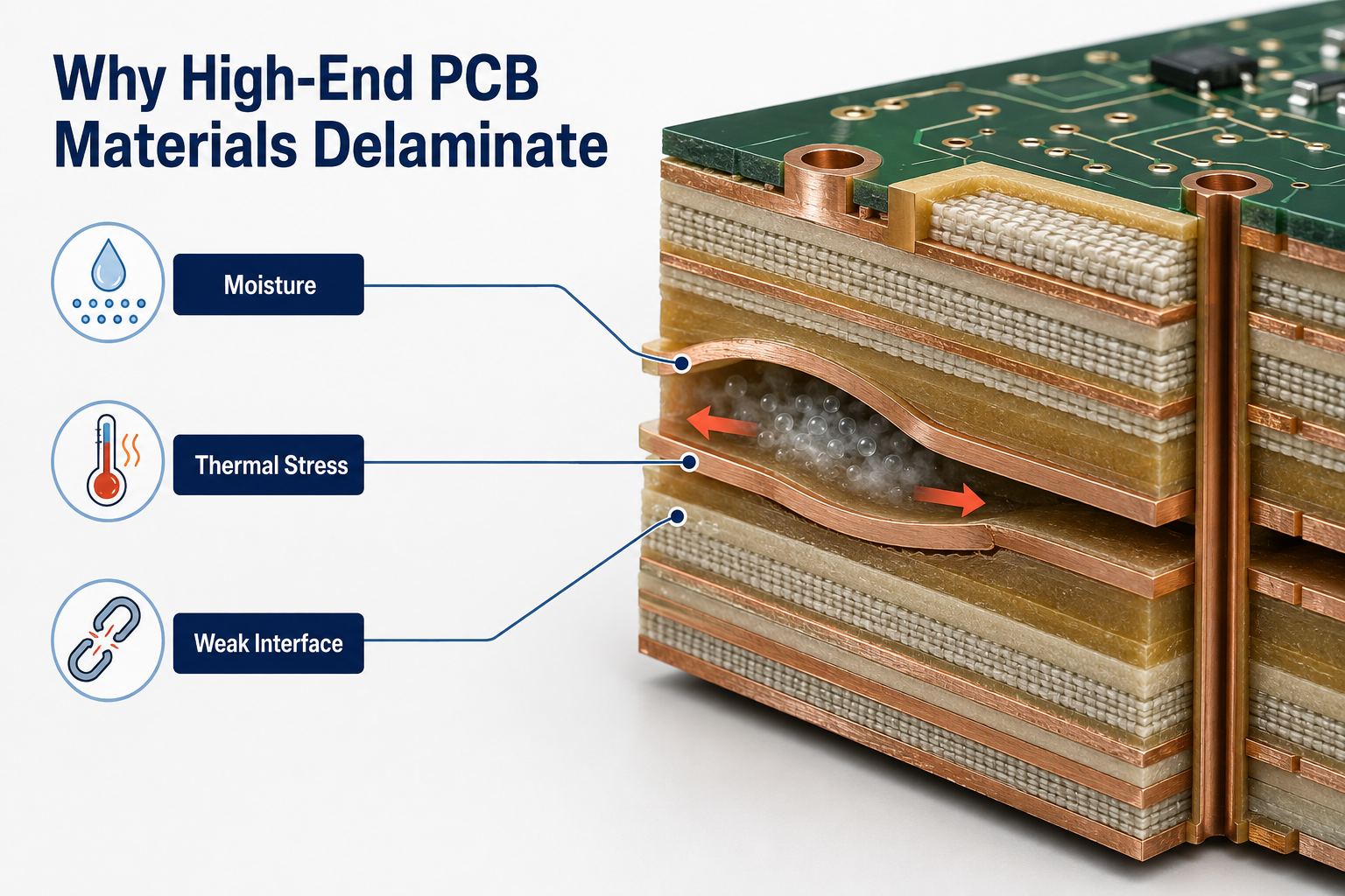
What Is PCB Delamination in High-End Materials?
PCB delamination in high-end materials is an interfacial or cohesive bond failure that separates layers which should remain permanently joined. The defect can be local or extensive and may appear as an internal void, a lifted copper feature, a surface blister, or separation near a via or board edge.
Delamination should not be confused with every pale or fibrous mark visible in a laminate. Measling and crazing describe different resin-glass conditions, while a blister is a localized raised area that may result from internal separation or trapped volatiles. A confirmed disposition should identify where the separation occurred and whether it interrupts a conductor, reduces insulation spacing, exposes a path for moisture, or weakens the structure.
| Observed Condition | Likely Location | Why It Matters |
| Surface blister | Solder mask, copper-to-dielectric, or near-surface laminate | May indicate trapped moisture, poor adhesion, or contamination |
| Internal planar separation | Core-prepreg or copper-resin interface | Can expand during thermal cycling and affect insulation or signal paths |
| Separation near a via | Resin, copper interface, or glass bundle beside the barrel | May combine with Z-axis stress and threaten via reliability |
| Edge separation | Routed edge or exposed laminate interface | Can admit moisture and propagate under later heating |
Why Can Advanced PCB Materials Delaminate?
Advanced PCB materials delaminate when the stress applied to an interface exceeds the bond strength available at that location. The initiating weakness can come from the material, storage, surface preparation, stackup design, lamination process, drilling and plating, assembly heating, or rework.
High-end constructions can make the margin narrower for several reasons:
- More interfaces: high layer counts create more bond lines and more opportunities for local contamination or incomplete wetting.
- Thin dielectrics and dense copper: resin must fill narrow spaces and compensate for uneven copper distribution without starving another area.
- Smoother copper: low-profile foil reduces conductor loss, but the selected treatment and resin system must still provide reliable adhesion.
- Multiple lamination cycles: sequential-build HDI boards expose earlier layers to repeated heat and pressure.
- Hybrid material systems: different resins, glass styles, copper treatments, and coefficients of thermal expansion may not move together during heating.
- Higher assembly temperature: lead-free reflow and repeated rework can consume the thermal margin of a weak bond.
The main PCB delamination causes are therefore interactive. Moisture alone may not damage a well-bonded construction, and one thermal excursion may not open a dry board. Moisture, a weak interface, and rapid heating together are far more dangerous.
How Do Moisture and Thermal Shock Start Delamination?
Moisture and thermal shock start delamination when absorbed water expands, vaporizes, or changes the mechanical behavior of the laminate faster than pressure can dissipate. During reflow or rework, vapor pressure acts on the weakest internal interface while copper, glass, and resin expand at different rates.
An IPC technical paper on moisture in PCB laminates reported that absorbed moisture reduced time-to-delamination performance for several evaluated materials. The same work explains that moisture affects swelling and Z-axis expansion. This supports a practical rule: thermal robustness must be evaluated in the conditioned state that represents handling and assembly, not only on a dry datasheet specimen.
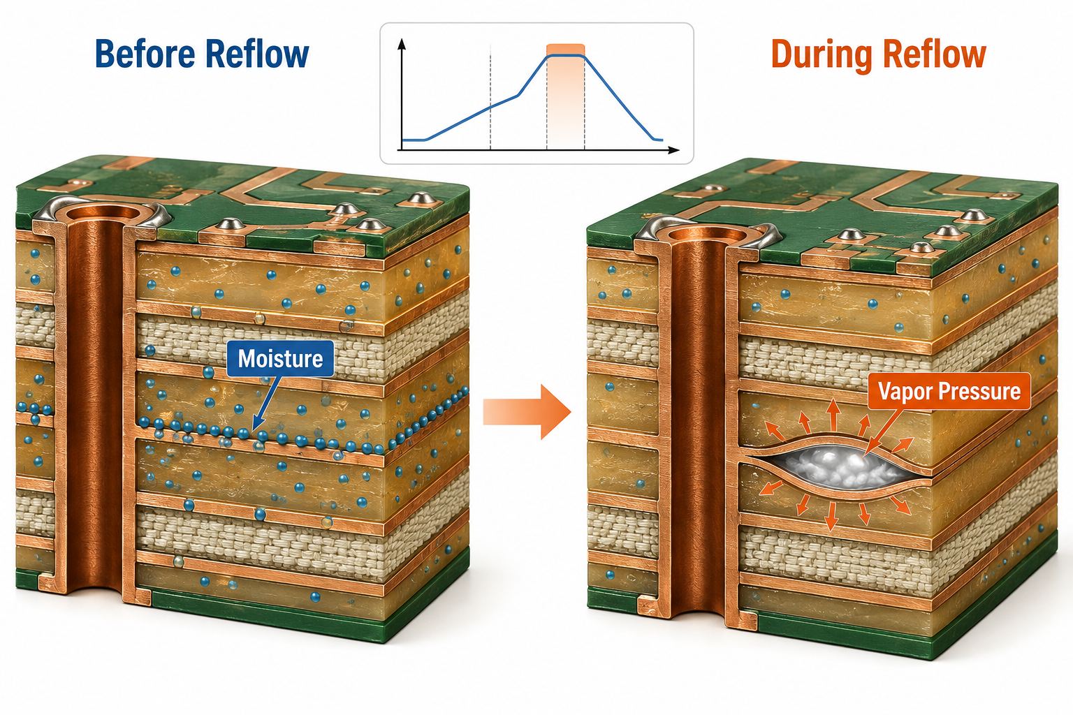
Common exposure paths include:
- unsealed laminate, prepreg, or finished boards stored in humid conditions;
- a long floor-life interval before assembly;
- aqueous processing followed by inadequate drying;
- rapid heating or an excessive reflow peak;
- multiple reflow, wave-solder, selective-solder, or hand-rework cycles;
- baking followed by poor packaging or renewed moisture exposure.
Baking can reduce moisture when the material and finish allow it, but it cannot restore a contaminated interface, replace missing resin, or repair an already separated bond. The bake condition must be approved for the board construction and surface finish.
How Do Lamination Parameters and Resin Flow Cause Weak Bonds?
Lamination parameters and resin flow cause weak bonds when the resin does not fully wet, fill, cure, and consolidate every interface in the stackup. The press cycle must match the actual resin system, panel mass, copper distribution, dielectric thickness, and number of layers.
- Insufficient flow can leave voids, glass stop, or resin-starved areas around heavy or dense copper.
- Excessive flow can squeeze resin away from a critical bond line and change finished dielectric thickness.
- Poor vacuum can leave trapped air or volatiles in a stack that appears flat externally.
- Incorrect heat-up rate can move the resin through its workable viscosity range before pressure and flow are balanced.
- Inadequate pressure may prevent full consolidation; excessive pressure may worsen resin loss or dimensional movement.
- Incomplete cure reduces thermal and chemical resistance, while an unsuitable cycle can embrittle or over-stress the system.
Prepreg selection must also provide enough resin to fill the designed copper topography. A technically advanced low-loss laminate can still fail if the chosen prepreg construction cannot fill a dense copper area without starving an adjacent region.
Why Do Surface Preparation and Copper Profile Matter?
Surface preparation and copper profile matter because adhesion depends on both chemical compatibility and the physical condition of the bonding surface. Oxidation, fingerprints, release residue, cleaning chemistry, dust, or excessive delay after treatment can reduce the bond strength before the stack enters the press.
High-speed boards often use smoother copper to reduce conductor loss. That does not mean smooth copper is unsuitable, but it leaves less room for an uncontrolled bonding process. The foil treatment, oxide alternative, resin chemistry, handling method, and lamination cycle must be qualified together.
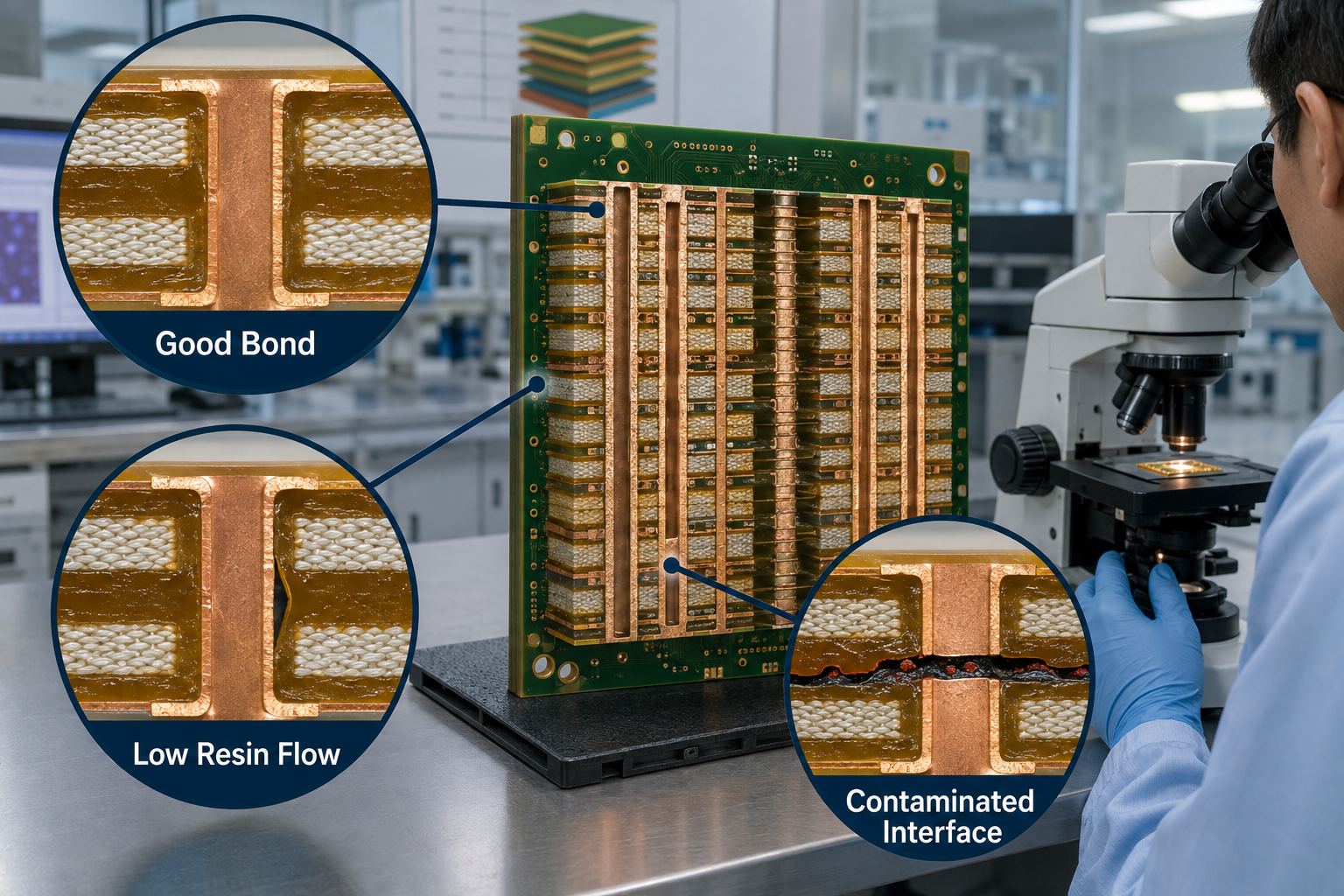
A useful failure analysis asks whether the separation is adhesive, at the copper-resin boundary, or cohesive, within the resin or reinforced dielectric. That distinction guides the corrective action. Increasing press pressure will not correct surface contamination, and extra cleaning will not fix a resin-volume shortage.
How Do Hybrid Materials and Repeated Lamination Add Risk?
Hybrid materials and repeated lamination add risk by combining interfaces with different thermal expansion, cure behavior, surface treatment, and thermal history. The construction may be electrically attractive but still require a narrower manufacturing window than a homogeneous stackup.
Before releasing a hybrid or sequential-lamination design, the fabricator should review:
- resin-system compatibility and supplier processing guidance;
- X-Y and Z-axis expansion through the expected thermal range;
- Tg, decomposition temperature, and time-to-delamination data;
- copper treatment and interlaminar adhesion;
- prepreg flow and fill across copper-density transitions;
- the total number of lamination and assembly heat cycles;
- drill, desmear, plasma, and plating chemistry compatibility.
Tg alone is not a sufficient selection rule. An IPC comparison of laminate thermal properties showed that time-to-delamination behavior did not simply follow Tg; decomposition temperature and the material system also mattered. The released requirement should therefore reflect the real thermal profile and reliability target.
What Does Delamination Look Like and How Is It Confirmed?
Delamination can look like a surface bubble, pale patch, lifted pad area, edge split, or local swelling, but internal separation may have no reliable external sign. PCB delamination images are useful for screening only; lighting, solder-mask color, glass weave, measling, and machining marks can make different defects look similar.
Confirmation should use methods appropriate to the suspected location:
- Visual and dimensional inspection: identifies blistering, bow, twist, edge separation, or surface change.
- Scanning acoustic microscopy: can map planar internal separations when equipment and board geometry allow.
- Microsection: destructively reveals the bond line, void, resin condition, copper interface, and nearby via structure.
- Thermal stress or simulated reflow: checks whether a latent weakness opens under the intended assembly exposure.
- TMA time-to-delamination: characterizes laminate response at a specified test temperature; IPC lists TM-650 method 2.4.24.1 for this measurement.
- Electrical and reliability testing: determines whether the defect has affected insulation, continuity, impedance, or via performance.
A PCB delamination cross section should be taken through the actual indication whenever possible. A clean section from a distant coupon cannot explain a localized production defect.
Can PCB Delamination Be Repaired?
PCB delamination repair is usually not acceptable for an internal structural separation in a high-reliability multilayer board. Injecting adhesive, pressing a blister flat, or baking the board may hide the symptom without restoring the qualified dielectric spacing, bond integrity, insulation performance, or long-term thermal reliability.
A limited external defect may sometimes receive an engineering disposition if the applicable drawing, acceptance standard, customer, and reliability assessment permit it. That decision should document the location, size, affected conductors, insulation distance, test evidence, and intended service environment. It should not be treated as a general repair method.
For confirmed internal delamination, the safer corrective path is normally to quarantine the lot, determine the failure interface, verify the extent, correct the root cause, and rebuild affected product. Rework without root-cause evidence can convert a visible manufacturing escape into a field failure.
How Should Fabricators Improve a Delamination Process?
Fabricators should improve a delamination process by linking the failure location to the process step that created the weak interface. Corrective action should be evidence-based and verified with a controlled build.
| Confirmed Cause | Immediate Improvement | Verification |
| Moisture before thermal exposure | Restore dry storage, packaging, exposure control, and an approved bake process | Moisture review plus representative reflow or thermal stress |
| Resin starvation or glass stop | Adjust prepreg construction, copper balancing, pressure, vacuum, and heat-up profile | Microsections across high- and low-copper-density areas |
| Contaminated or degraded surface | Correct cleaning, surface treatment, rinsing, drying, and hold-time control | Bond assessment, peel testing where applicable, and thermal exposure |
| Hybrid-material mismatch | Reassess compatibility, CTE, cure, thickness, and thermal history | Qualification panels using the production stackup |
| Assembly or rework overheating | Correct the thermal profile and limit cumulative excursions | Profile records and post-process inspection |
The verification build should use production-intent material lots, copper distribution, panel format, lamination equipment, and assembly exposure. A laboratory coupon that removes the difficult geometry may prove the resin can bond, but not that the released PCB can be manufactured consistently.
How Can Designers and Buyers Prevent PCB Delamination?
Designers and buyers prevent PCB delamination by defining the material system, thermal exposure, and acceptance evidence before the quotation is locked. Early collaboration gives the fabricator room to adjust prepreg, copper balance, and the lamination sequence without changing finished electrical requirements.
- Share the real thermal history. Include all lamination, reflow, wave, selective-solder, press-fit, coating cure, and expected rework cycles.
- Approve exact materials and alternates. Do not authorize substitution by a broad “equivalent high-Tg” note.
- Review copper balance and resin demand. Large copper-free zones beside dense planes require deliberate fill planning.
- Set storage and floor-life controls. Define packaging, humidity exposure, resealing, and any allowed bake process.
- Use production-intent prototypes. Qualify the same material family, stackup, and critical process sequence planned for volume.
- Specify evidence. Require the appropriate microsections, thermal stress, reflow simulation, coupons, traceability, and change notification.
For designs where thin dielectrics and sequential lamination raise the risk, our HDI PCB fabrication guide explains the build-up context. For electrical geometry that must remain stable after material or thickness changes, see our impedance control PCB guide.
What Should Be Included in a Delamination Control Plan?
A delamination control plan should translate the risk into measurable incoming, fabrication, assembly, and verification controls. At minimum, it should record:
- approved laminate, prepreg, copper, and surface-treatment combinations;
- material storage, packaging, exposure, and bake conditions;
- prepreg resin content and fill assumptions for the released copper pattern;
- surface preparation, hold time, and contamination controls;
- vacuum, pressure, temperature, heat-up, dwell, and cooling windows;
- sequential lamination and cumulative assembly heat cycles;
- inspection sampling locations and acceptance criteria;
- material-lot and process traceability;
- the response plan for blistering, separation, or an abnormal microsection.
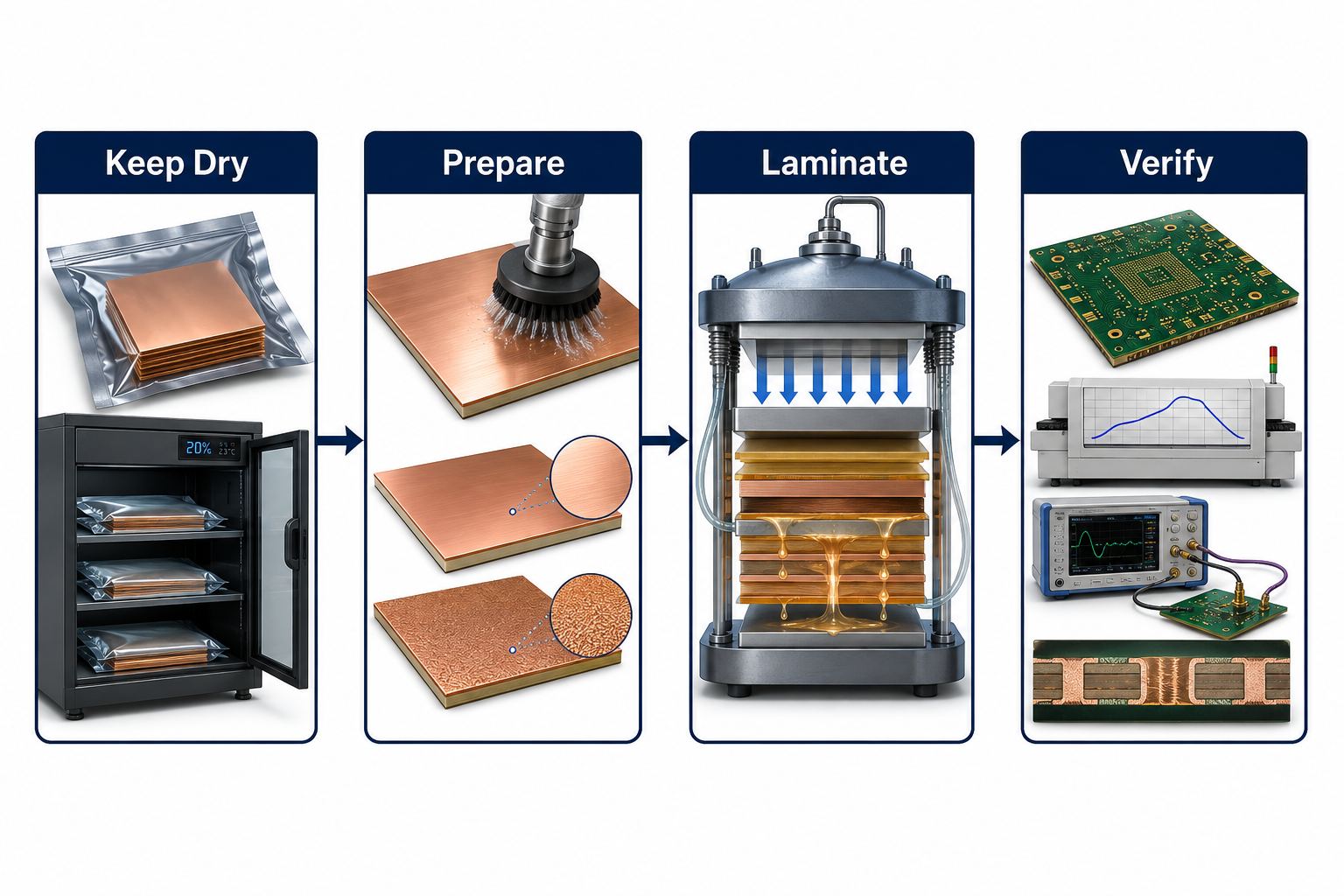
The plan should also define who can approve a material, stackup, or process change. If availability forces a substitution, production should pause at the approval gate rather than silently consume a different construction.
Frequently Asked Questions About PCB Delamination
What causes PCB delamination?
The immediate cause is stress exceeding local bond strength. Common contributors include moisture, rapid heating, inadequate resin flow, incomplete cure, contaminated surfaces, incompatible materials, repeated thermal cycles, and excessive rework.
Does a higher Tg prevent delamination?
No. Tg is important, but it does not describe moisture behavior, decomposition, time-to-delamination, copper adhesion, resin flow, or the quality of the fabricated bond line.
Can baking fix an already delaminated PCB?
No. An approved bake may remove moisture before heating, but it does not restore an interface that has already separated or correct contamination and resin starvation.
Why does delamination appear after reflow instead of during PCB fabrication?
A weak interface may remain closed and invisible after lamination. Reflow adds rapid thermal expansion and vapor pressure, exposing the latent defect.
Can AOI or X-ray always find internal delamination?
No. AOI examines visible surfaces, and standard transmission X-ray may not clearly reveal a planar separation. Acoustic imaging, targeted microsectioning, and thermal verification are often more informative.
Are low-loss PCB materials inherently prone to delamination?
No. They require a compatible copper treatment, prepreg construction, lamination cycle, handling method, and assembly profile. A qualified process can produce reliable low-loss multilayer boards.
How Can EBest Circuit Help Prevent PCB Delamination?
At EBest Circuit, we can review your Gerber files, stackup, laminate and prepreg callouts, copper distribution, via structure, target impedance, assembly profile, quantity, and inspection requirements before fabrication. We use those inputs to identify moisture, resin-fill, material-interface, and thermal-cycle risks that should be closed before production.
Send the released data and your reliability requirements to sales@bestpcbs.com. We will return the engineering questions, proposed stackup controls, and verification items needed for a manufacturable high-end multilayer PCB.
You may also like







Tags: pcb delamination, pcb delamination causes, pcb delamination cross section, pcb delamination images, pcb delamination repair