PCB via filling plays a significant role in modern circuit manufacturing as devices continue to shrink and performance demands rise. Today’s designs rely on tighter spacing, finer pitches, and denser multilayer structures. Because of this trend, many teams are searching for practical guidance on PCB via filling, via filling in PCB, via fill PCB, and the overall PCB via hole filling process. As more circuits require stable pads, improved thermal transfer, and reliable current paths, filled via PCB structures have become a vital part of HDI and advanced board fabrication.
This guide explains what filled vias are, why they matter, how the materials differ, and how to select the right method for your application. It also provides a complete overview of the PCB via filling process, a comparison between via plug and via fill, design considerations, typical cost ranges, and the questions users ask most often.

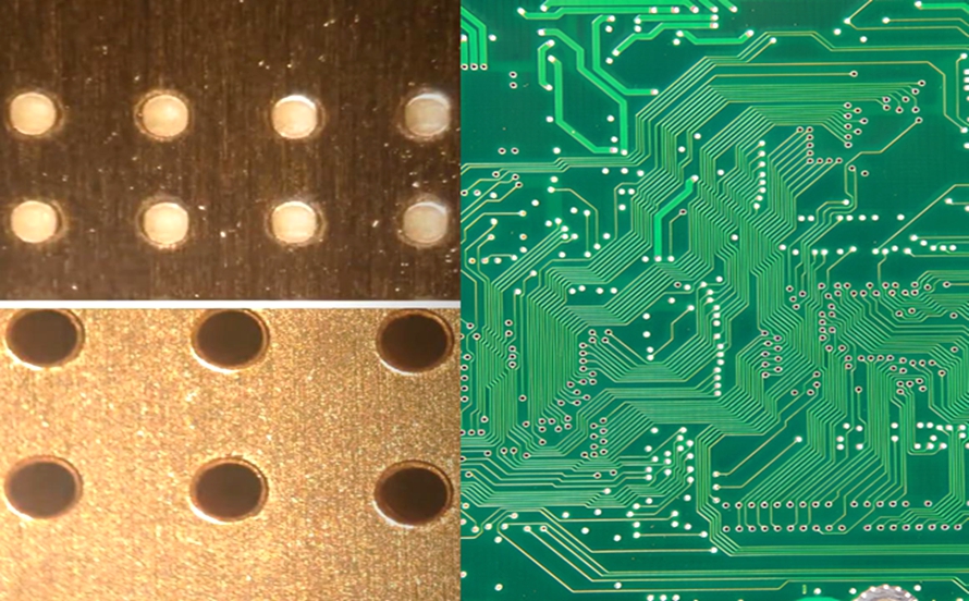
What Is Via Filling in PCB?
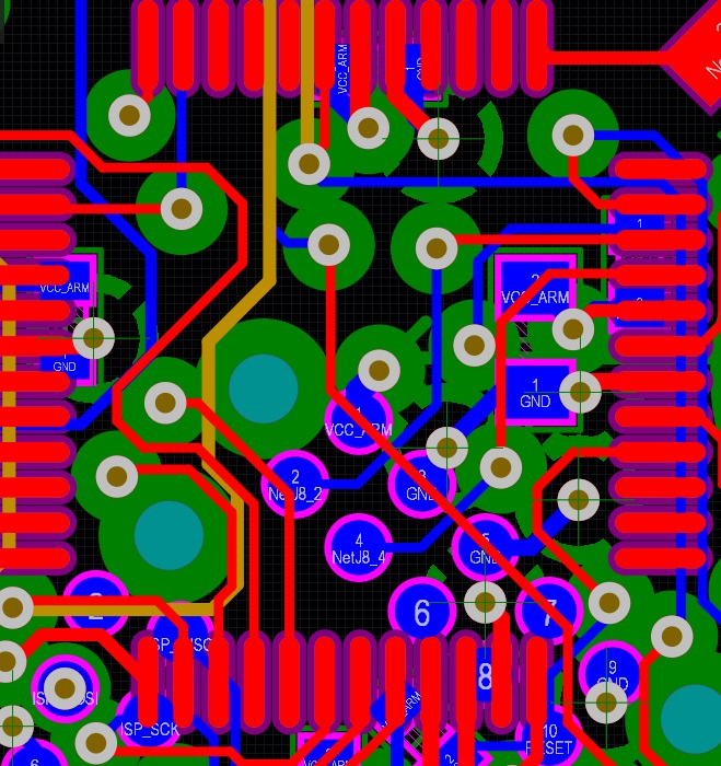
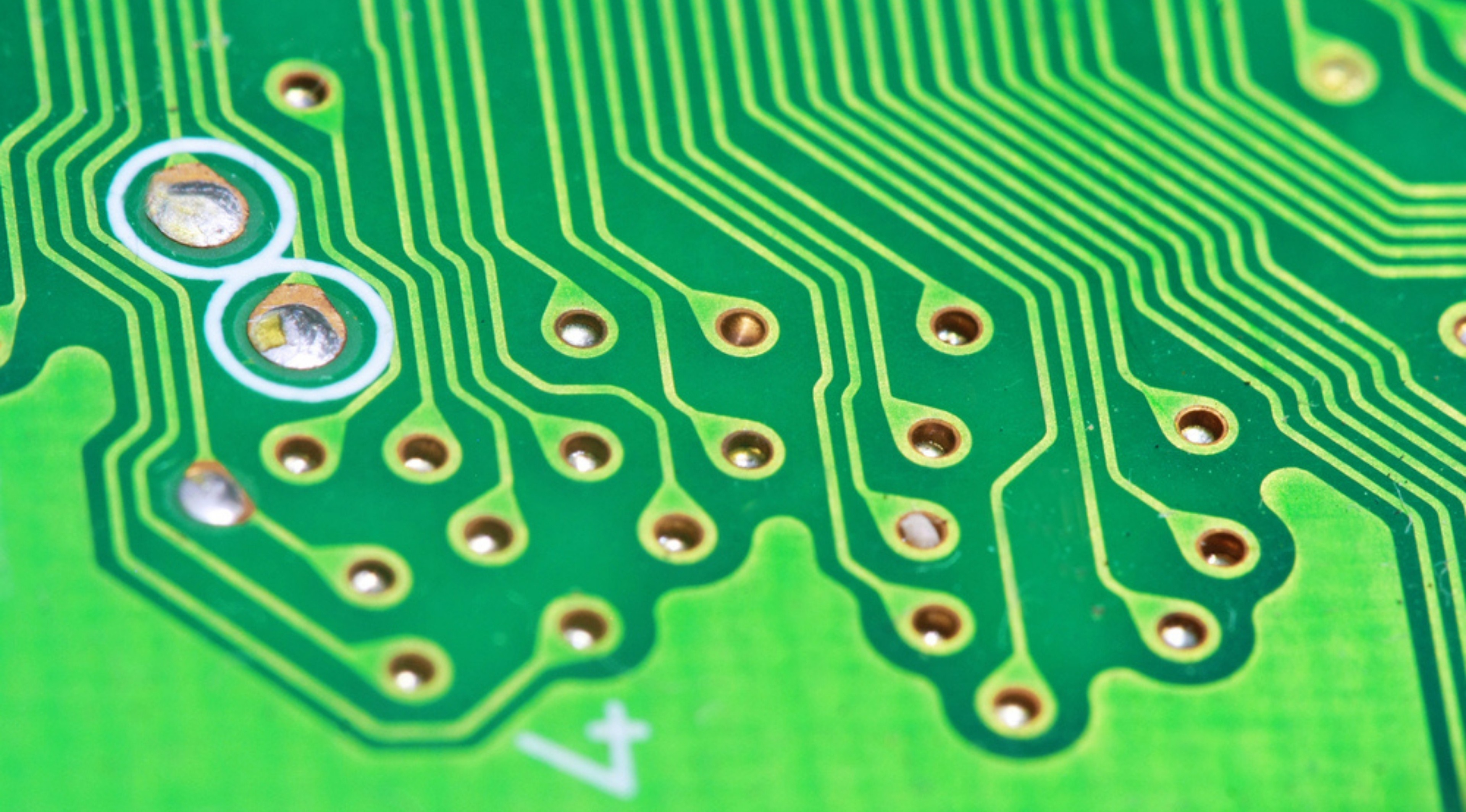
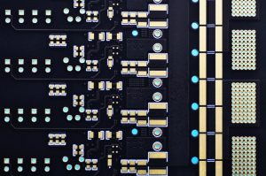
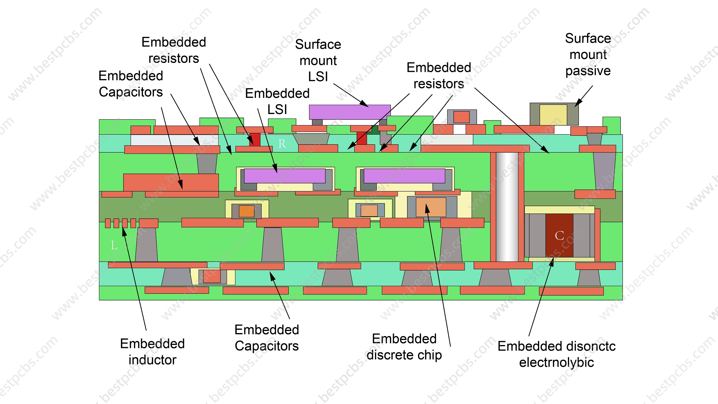
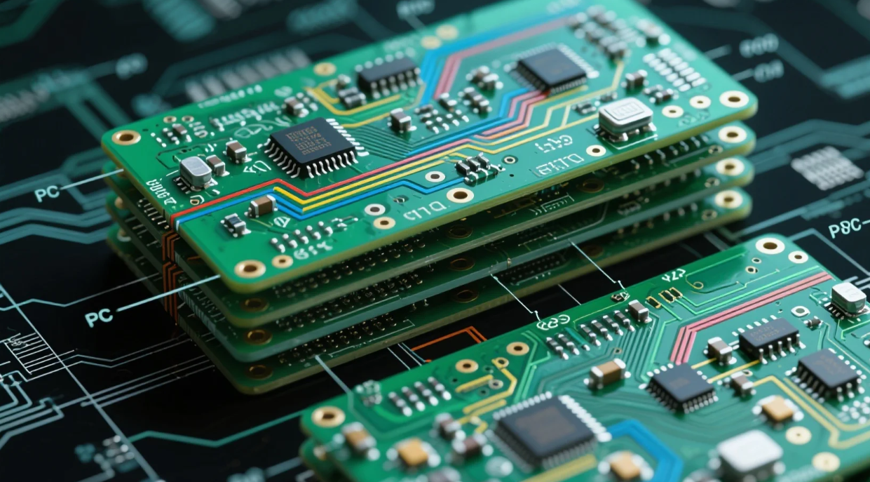
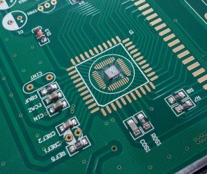
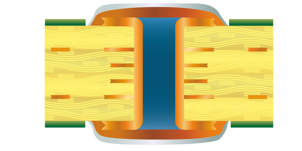
Via filling in PCB refers to the process of depositing conductive or non-conductive material into a drilled hole so the entire via barrel becomes a solid structure. The goal is to create a stable foundation for surface plating, improve mechanical strength, and prevent solder from flowing into the via during assembly. Because advanced designs frequently place vias directly under BGA pads or inside high-speed routes, a smooth and solid surface is essential to support soldering, routing, and long-term reliability.
As manufacturing continues to evolve, PCB via filling now appears in smartphones, automotive modules, industrial controls, medical devices, RF boards, and many other high-performance applications. Instead of leaving the via hollow, the fill material enhances thermal transfer, reduces voids, strengthens the structure, and ensures a consistent surface throughout production.
Why Do PCB Via Filling?
Advantages of PCB Via Filling:
- Enhanced Soldering Quality: Filled vias eliminate the risk of solder wicking into a via barrel. This creates a stable pad surface, especially for fine-pitch BGA or QFN packages where even small voids can cause long-term instability.
- Improved Thermal Path: Conductive via fills assist heat transfer from power devices to internal or external copper layers. This is valuable in power management modules, LED boards, and RF power amplifiers.
- Higher Mechanical Strength: Filled vias support the surrounding copper pad during thermal cycling, bending stress, or reflow heating. This is vital in thin multilayer constructions.
- Increased Routing Flexibility: With filled vias PCB structures, routing can pass through pad-in-via areas without compromising solder joints. This allows compact layouts and shorter trace lengths.
- More Reliable Multilayer Connectivity: A filled via barrel has improved consistency because it removes air pockets and reduces plating defects. This directly improves reliability in high-frequency, automotive, and aerospace circuits.
What Material Is Used for PCB Via Filling?
| Filling Material Type | Advantages | Applications | Cost |
| Non-Conductive Epoxy | Stable performance, cost-effective, smooth via-in-pad surface | HDI boards, smartphones, tablets, consumer electronics, BGA via-in-pad | Low |
| Conductive Epoxy | Enhanced thermal/electrical conductivity | Power modules, LED drivers, thermal pads, high-power compact circuits | Medium–High |
| Copper Filling (Electroplated) | Optimal electrical/thermal performance, high reliability | RF boards, automotive circuits, aerospace PCBs, high-speed digital designs | High |
| Resin/Polymer Blend | Mechanical stability, low dielectric loss, thin stack-up compatibility | Flexible circuits, rigid-flex designs, hybrid materials, ultra-thin layers | Medium |
| Solder Mask Plug | Low-cost moisture barrier, prevents solder wicking | General PCBs, non-HDI boards, low-to-mid density layouts | Very Low |
What is the Difference between Via Plug and Via Fill?
| Category | Via Plug | Via Fill |
| Structure | Partially blocks via, leaving hollow space | Fully fills via barrel, no hollow space |
| Material | Resin or solder mask | Epoxy, conductive material, or copper plating |
| Surface Appearance | May have slight depressions | Creates flat pad, suitable for via-in-pad |
| Purpose | Prevents solder flow, protects barrel | Supports fine-pitch routing, enhances reliability |
| Thermal Performance | Limited heat transfer | Improved heat transfer (especially with conductive/copper fill) |
| Cost Level | Lower cost | Higher cost (varies by fill method) |
| Common Use Case | General PCB, low-to-mid density designs | HDI, BGA pads, RF boards, power modules |
Design Consideration for PCB Via Filling
Below Are PCB Via Filling Design Consideration:
1. Clarify Filling Purpose
- Determine the requirement first: whether it is to enhance thermal conductivity (e.g., power device heat dissipation), improve signal integrity (reduce impedance discontinuity), strengthen mechanical structure (prevent vibration cracking), or be compatible with subsequent processes (e.g., embedded capacitance). Different objectives correspond to different material and process selections to avoid ineffective costs.
2. Prioritize Conductive Filling
- For high-frequency/high-speed signals, conductive filling (e.g., silver paste, copper paste) can reduce via impedance to below 1Ω, minimizing signal reflection and crosstalk. Resin filling is only suitable for non-critical signals or mechanical reinforcement to avoid abnormal parasitic parameters caused by insulation.
3. Control Aperture and Aspect Ratio
- For small apertures (≤0.2mm), evaluate filling capability: aspect ratios >6:1 may cause voids, recommend vacuum filling or special processes (e.g., capillary plating). For large apertures, control filling layer thickness to avoid delamination due to mismatched thermal expansion coefficients.
4. Validate Material Compatibility
- Filling materials must be compatible with substrates (e.g., FR4, high-frequency materials) and surface finishes (e.g., ENIG, OSP). For instance, epoxy resin filling requires thermal matching testing with solder to prevent thermal cycle cracking. Conductive pastes need verification for electromigration risks with adjacent conductors.
5. Design Thermal Dissipation Path
- For devices with thermal power >1W, via arrays must directly connect to thermal pads/copper planes. Filling material thermal conductivity should exceed 2W/(m·K) (e.g., modified epoxy + thermal fillers). Avoid isolated via groups causing local hot spots.
6. Define Process Window
- Require PCB manufacturers to provide filling process parameters: filling pressure (0.3-0.5MPa), curing temperature (150-180°C), and time (30-60 minutes). Critical parameters should be included in design specifications to prevent quality variations across batches.
7. Void Detection Standards
- Use X-ray/CT to inspect filling rate, requiring <5% void ratio. Critical signal vias need cross-section validation for filling continuity. Detection criteria must be mutually agreed upon with PCB manufacturers to avoid disputes.
8. Optimize Impedance Continuity
- Post-filling via impedance must match transmission lines (e.g., 50Ω microstrip requires via impedance ≤55Ω). Simulate to verify filling impact on S-parameters, preventing signal degradation due to impedance discontinuity.
9. Balance Cost and Reliability
- Conductive filling costs 3-5 times more than resin filling. Select based on product positioning: consumer products may partially fill critical vias, while industrial/automotive products require full filling in high-reliability areas. Avoid over-designing to prevent cost escalation.
10. Document Design Rules
- Specify in PCB design specifications: filling area marking (e.g., Via-in-Pad requires full filling), minimum spacing (filling area ≥0.2mm from pads), and test point reservation (avoid filling covering test pads). Ensure consistent information across design and manufacturing stages.
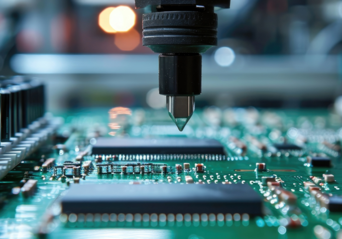
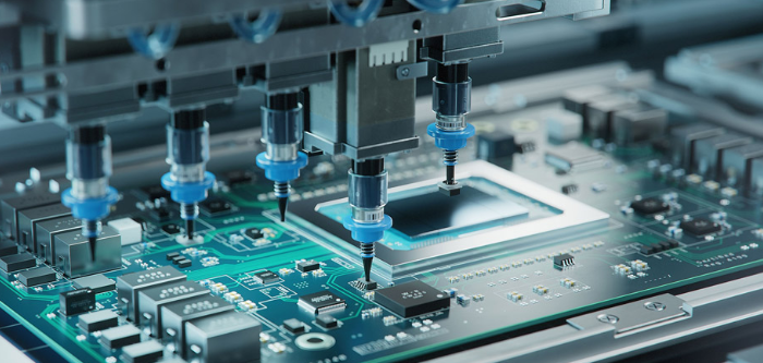
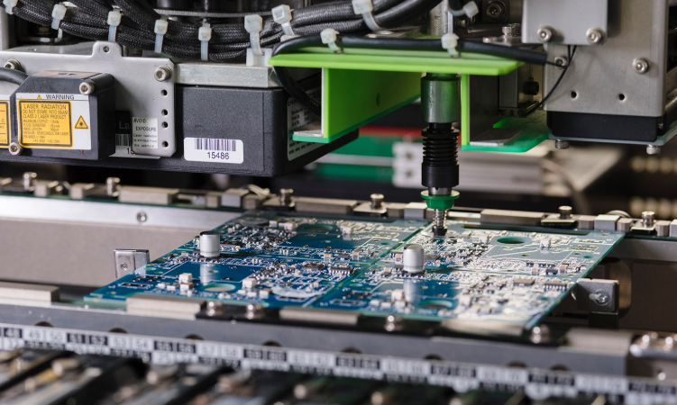
How to Fill in Via PCB?
Below Are Steps to PCB Via Filling Process:
- Select Filling Material Based on Application Needs: Use conductive materials (e.g., copper paste, silver-loaded epoxy) for high thermal/electrical conductivity in power-heavy designs; opt for non-conductive resins (e.g., epoxy) to prevent solder wicking in via-in-pad structures or improve surface flatness.
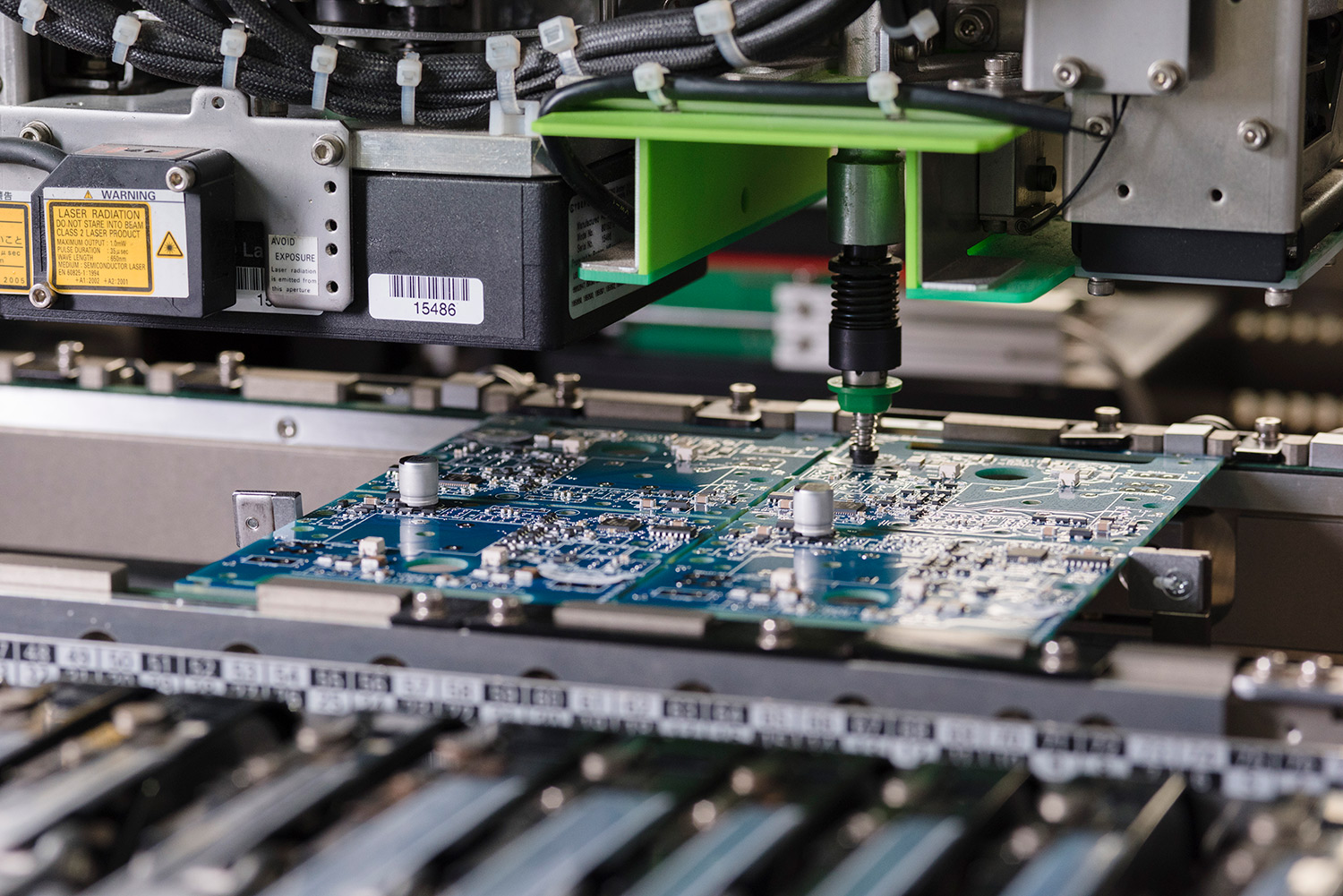
- Drill and Clean Vias: Ensure precise drilling with appropriate aspect ratios (hole diameter vs. thickness) to avoid filling defects. Clean via walls via plasma treatment or brushing to remove contaminants and promote material adhesion.
- Electroplate Hole Walls: Apply a thin copper layer to via walls using acidic copper plating solutions with organic additives to ensure robust electrical connections and prepare for filling material anchoring.
- Fill Vias with Specialized Material: Inject conductive/non-conductive pastes (e.g., TAIYO THP-100 DX1 for resin) using automated equipment to achieve complete filling without voids. For via-in-pad, use liquid photo-imageable solder mask (LPI) cured via UV exposure to create solid plugs.
- Planarize and Cure: Grind filled vias to achieve surface roughness <0.3μm via mechanical polishing. Cure filling materials at controlled temperatures (e.g., 150°C for 1.5 hours) to solidify and ensure structural integrity.
- Surface Finishing: Apply capping plating (e.g., nickel-gold) over filled vias to protect against oxidation and enable reliable soldering. Use solder mask tenting or plugging to prevent contamination and electrical shorts.
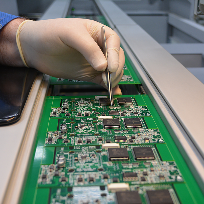
- Perform Quality Verification: Conduct electrical testing (e.g., continuity checks) and visual inspection to verify filling integrity, absence of voids, and proper surface finish. Ensure compliance with IPC-4761 standards for via protection types (e.g., VII-type for filled/capped vias).
How Much Does it Cost to Fill a Via?
The cost of PCB via filling varies according to material, hole size, density, and HDI level. Below is a price range for per via filling:
- Non-conductive epoxy fill: $0.008 – $0.03 per via.
- Conductive epoxy fill: $0.03 – $0.10 per via.
- Copper-filled via: $0.08 – $0.25 per via.
Depending on your design, filled vias may increase board cost by 10% to 30%. Projects with hundreds of via-in-pad locations require tighter process control, which can raise the price further.
FAQs of PCB Via Filling
Q1: Should via-in-pad always use filling instead of tenting?
A1: For fine-pitch BGAs or QFNs, filling is strongly recommended. It prevents solder voids and ensures a flat pad. Larger pad sizes may use tenting.
Q2: Why do some filled vias still show small dimples?
A2: Dimples appear when plating thickness or resin expansion is not perfectly balanced. High-precision factories use controlled planarization to avoid these marks.
Q3: Is filled via PCB helpful for high-speed signals?
A3: Yes. Filled vias remove air gaps and improve impedance uniformity. This helps maintain signal stability in high-speed routing.
Q4: Can filled vias improve heat dissipation in compact boards?
A4: Yes. Conductive and copper-filled vias move heat more efficiently from hot components to inner layers or copper planes.
Q5: Does filled via PCB increase production time?
A5: Usually it adds 1–3 days for non-conductive epoxy and 3–5 days for copper filling. The added time supports reliability and stability.