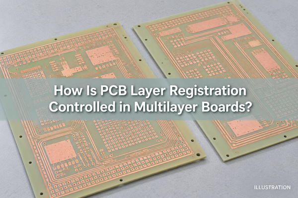
PCB layer registration is the positional alignment of copper features on different layers of a printed circuit board. If an inner-layer pad shifts away from its intended location, a drilled hole can leave too little copper around the barrel, even when the external artwork looks correct. Reliable multilayer fabrication therefore depends on controlling both copper-layer alignment and the relationship between the laminated stack and the drilling coordinates.
What Is the Difference Between Layer Registration and Hole Registration?
Layer-to-layer registration compares copper features on different layers; hole registration compares a hole with the copper features it must connect to or avoid. The two are related, but they are not interchangeable measurements.
| Registration check | Features being compared | What an error can affect |
|---|---|---|
| Layer-to-layer | Copper targets, pads or patterns on separate layers | Pad overlap, coupled routing and local clearances |
| Drill-to-copper | Drilled hole center and copper pad or clearance center | Remaining annular ring, breakout or unintended plane contact |
| Solder-mask-to-copper | Mask opening and surface pad | Exposed copper and mask coverage |
| Component placement | Component terminals and outer-layer land pattern | Assembly alignment, not internal copper alignment |
For PCB layer to layer registration, the drawing must identify the reference layer or datum and the features being measured. Comparing every layer with a common reference is not the same as reporting the largest separation between any two layers. A board can meet one stated limit and fail another if the measurement definitions differ.
What Causes PCB Layers to Become Misaligned?
Misalignment can begin before lamination and change during pressing. Etched cores can change dimensions as copper is removed, while temperature, moisture condition, material direction and processing history affect dimensional stability. Tooling wear, incorrect lay-up orientation or movement during bonding can add further error.
The shape of the error matters as much as its maximum value:
| Observed pattern | Possible explanation to investigate | Useful comparison |
|---|---|---|
| Similar offset at several targets | Translation or datum mismatch | Target coordinates against the same origin |
| Offset changes direction across the panel | Rotation | Targets near opposite panel edges |
| Offset grows with distance from the center | Scale change | X and Y spans before and after processing |
| Different local errors remain after global alignment | Nonuniform distortion | Multiple targets across the usable panel |
These patterns guide investigation; they do not identify the root cause by themselves. For example, shifting the drilling origin can reduce a uniform offset but cannot remove local distortion already locked into a laminated board.
How Does Layer Misregistration Affect Annular Ring?
Misregistration reduces the narrowest copper ring around a hole. For a circular pad and circular drilled hole, a simple geometric estimate is:
Minimum remaining ring = (minimum pad diameter − maximum drilled-hole diameter) / 2 − center offset
The diameters and offset must describe the same manufacturing stage. A finished plated-hole diameter is smaller than the drilled opening; substituting it without accounting for plating can overstate the copper margin.
Consider a 0.60 mm pad and a 0.30 mm drilled opening, ignoring diameter tolerances for this example:
| Center offset | Narrowest remaining ring |
|---|---|
| 0.00 mm | 0.150 mm |
| 0.05 mm | 0.100 mm |
| 0.10 mm | 0.050 mm |
| 0.15 mm | 0.000 mm: geometric tangency |
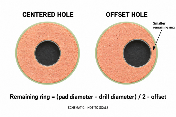
These values illustrate geometry, not an acceptance specification. Etched pad size, drill size variation, layer movement and drilling position all consume margin. Internal clearances matter too: a shifted hole can approach a plane that it should not contact, even if its connected pad retains copper.
What PCB Layer Registration Tolerance Should You Specify?
Specify the tolerance together with its reference, measurement method and affected layer pairs. There is no single PCB registration tolerance that can be applied to every stack-up simply by counting layers or naming an acceptance class.
For a PCB layer to layer registration tolerance, clarify:
- Whether the limit is layer-to-layer, drill-to-pad, or a combined manufacturing allowance.
- Whether it is a radial displacement or separate X and Y limits.
- Which targets, layers and panel locations are measured.
- Whether the result applies before lamination, after lamination or after drilling.
- The applicable specification revision, product class and drawing requirements.
An X/Y allowance is not automatically a radial allowance. If both axes permit 0.05 mm simultaneously, the resulting diagonal displacement can reach approximately 0.071 mm. If the intended limit is a 0.05 mm radius, the drawing should say so.
PCB layer registration tolerance must leave adequate copper and clearance at the actual minimum geometry. For Class 2 boards, layer-to-layer registration must be evaluated against the applicable acceptance criteria and the agreed fabrication requirements together. The geometric example above is not an IPC limit, and a class designation alone is not a complete positional tolerance specification.
How Are Inner Layers Aligned Before Lamination?
Inner-layer registration uses features tied to the copper artwork, followed by a controlled method of positioning the cores in the lay-up. Optical registration equipment can locate etched targets and establish tooling holes relative to the actual pattern rather than relying only on the cut edge of the laminate.
Inspection before bonding is equally important. Inner-layer AOI compares the visible etched pattern with the design data to detect defects while the copper is accessible. Correct layer identity, orientation and sequence must then be maintained through lay-up. A perfectly aligned but incorrectly oriented core is still wrong.
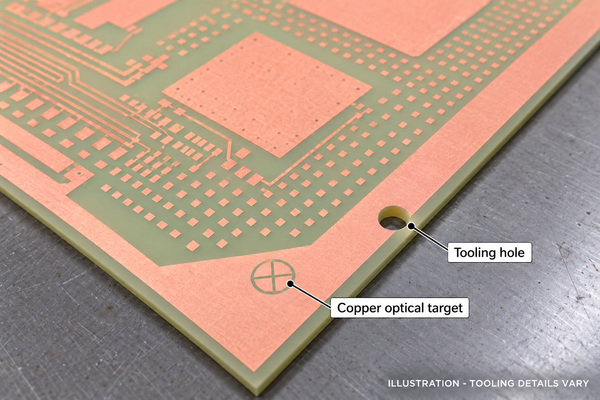
Tooling holes and optical targets perform different jobs: one physically locates material; the other provides a measurable reference to the artwork. Their size, shape and position belong to the fabrication tooling scheme and should not be copied from an unrelated board.
How Does Lamination Affect Layer Alignment?
Lamination subjects the lay-up to heat, pressure and resin flow. Material movement during this stage can alter the alignment established at loading. Dimensional compensation therefore needs to reflect the selected laminate, copper distribution and process history, rather than one scaling factor used for every job.
In multilayer PCB design, stack-up symmetry and balanced copper distribution help control dimensional behavior and warpage. They do not guarantee registration on their own. A multilayer PCB stackup also needs consistent material orientation, compatible cores and prepregs, and a controlled bonding sequence.
For an 8 layer PCB, for example, reviewing all internal cores and their target positions provides more information than checking only the two outer layers. Common PCB stackups provide a starting point, but the approved material construction and panel arrangement determine the actual manufacturing route. Sequentially laminated structures require attention to the dimensional changes accumulated over multiple bonding cycles.
How Is X-Ray Used to Check PCB Layer Registration?
X-ray inspection can reveal internal copper reference features after lamination, when an optical camera can no longer see them directly. A suitable target design and measurement setup allow the positions of internal features to be compared and can support the choice of drilling references.
The result depends on what the image separates clearly. Overlapping targets, unsuitable geometry or insufficient resolution can make individual layers difficult to distinguish. Reporting a single position from an ambiguous image does not prove that every layer is within tolerance.
X-ray-guided drill registration can optimize drilling relative to the bonded copper stack. It cannot move copper layers that are already laminated together. If different layers have shifted in different directions, the selected drill position may be a compromise; inadequate remaining margins still require disposition.
What Can AOI, Microsections and Electrical Testing Confirm?
These methods answer different questions. None should be treated as a complete substitute for the others.
| Method | Useful evidence | Important limitation |
|---|---|---|
| Inner-layer AOI | Visible copper pattern defects before bonding | Does not show final post-lamination layer positions |
| X-ray registration measurement | Internal target positions in the laminated stack | Requires identifiable targets and suitable resolution |
| Microsection | Local hole-wall, pad and interconnection geometry | A selected section may not intersect the worst offset direction |
| Electrical testing | Opens and shorts covered by the test | Does not quantify remaining annular-ring margin |
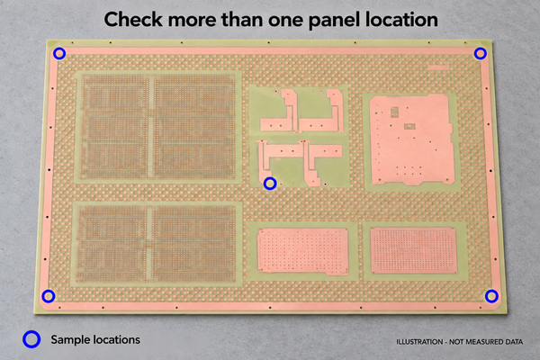
When a registration concern is investigated, identify the panel, coupon location, layer pair, datum and measurement direction. A microsection through one hole at one location is local evidence; it should not silently become a claim about every hole on the panel. Likewise, passing continuity does not show how much manufacturing margin remains before breakout.
How Can PCB Design Reduce Registration Risk?
Provide room for the expected manufacturing variation before routing becomes too dense to change. The most useful multilayer PCB design guidelines connect pad and clearance geometry to the proposed fabrication route:
- Review pad sizes and antipad clearances using the drilled-hole requirements, not only the finished-hole size.
- Keep the artwork, drill files, layer order and stack-up revision consistent.
- Evaluate narrow internal clearances and small capture pads early in DFM.
- Agree on controlled features and registration acceptance before tooling is finalized.
- Recheck the margins if material, panelization, via construction or lamination sequence changes.
Our multilayer PCB manufacturing supports FR4 constructions up to 32 layers, subject to the selected structure and engineering review. Layer count alone does not define the achievable registration tolerance.
For HDI PCB manufacturing, small capture features and sequential build-up make registration especially relevant. We support fine-line HDI designs down to 2/2 mil under applicable manufacturing conditions; this line/space capability is not a promise of a particular layer-position tolerance.
Layer alignment can also matter to impedance-controlled PCBs, particularly where coupling depends on the overlap of conductors on different layers. A simple shift over a wide continuous reference plane does not have the same effect as a shift between broadside-coupled traces. Review the actual structure rather than assuming every offset produces the same impedance change.
What Files Are Needed to Review Layer Registration?
At EBest Circuit (Best Technology), we provide PCB fabrication and DFM support. Send us the complete fabrication data, layer order, proposed stack-up, drill information and drawing tolerances so we can evaluate the construction before production.
For a specific layer-registration requirement, include the affected layers or vias, intended datum, acceptance criteria and any requested inspection records. If a previous lot showed an offset, its measured coordinates and sample location are more useful than an unscaled photograph alone. We will confirm feasible requirements and the agreed inspection scope for the proposed board; do not assume a generic capability value applies to every layer pair.
PCB Layer Registration FAQs
1. Are SMT fiducials the same as inner-layer registration targets?
No. SMT fiducials locate a board or component region for assembly equipment. Inner-layer targets support fabrication alignment or measurement. Their purposes and manufacturing stages differ, even if both use recognizable copper shapes.
2. Can an electrical test pass when layer registration is poor?
Yes. A connection may remain continuous while its annular-ring margin is reduced. Electrical test results and geometric acceptance need to be evaluated separately.
3. Can registration be checked on a finished assembled PCB?
Some internal features may be examined with suitable X-ray equipment, but components, shields and overlapping copper can limit interpretation. Fabrication targets or coupons and production-stage records are usually more useful for investigating a specific layer-pair offset.
4. Does adding more copper to a pad always solve misregistration?
No. A larger pad can improve hole capture, but it can reduce spacing to neighboring copper and change routing or electrical behavior. Correct the error source and review both connection margin and isolation clearance.
For a PCB layer registration review, send your fabrication package and critical feature requirements to sales@bestpcbs.com. We can assess the multilayer construction and clarify the manufacturing and inspection requirements before you release the board.
You may also like






Tags: Multilayer PCB, PCB Layer Registration, pcb manufacturing