PCB manufacturing PCB manufacturing
Home > Blog

Log Periodic Dipole Array Antenna PCB: Design and Fabrication

August 21st, 2026

A Log Periodic Dipole Array Antenna PCB prints a sequence of scaled dipole elements and its feed structure on a circuit-board substrate. It can provide directional, wideband operation, but its final response depends on the complete geometry, laminate, copper, feed transition, connector, and nearby mechanical environment.

The first geometry calculation is only a starting point. A production-ready design must also control dielectric data, conductor dimensions, the balanced feed, the coax transition, board outline, surface treatment, and the measurement reference plane. This guide connects those antenna decisions to PCB fabrication and verification.

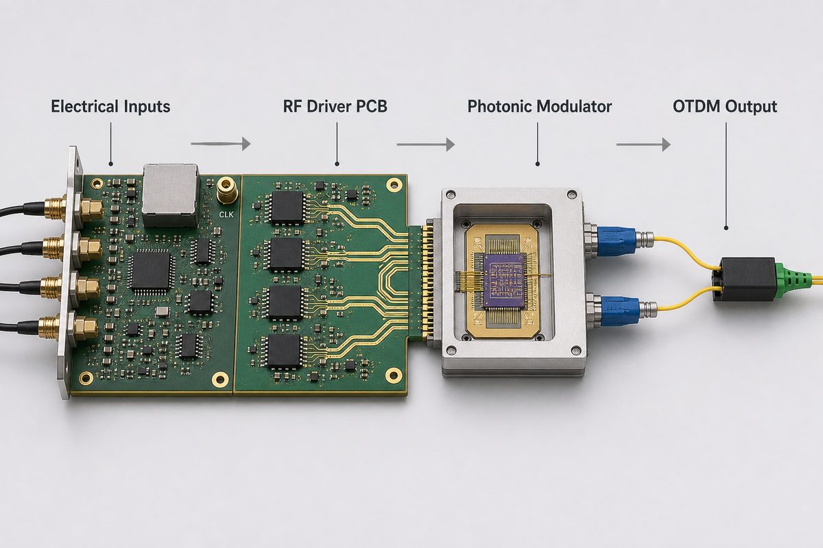
Log Periodic Dipole Array Antenna PCB with progressively scaled copper dipoles and an SMA feed

What Is a Log Periodic Dipole Array Antenna PCB?

A printed LPDA is a broadband directional antenna formed by multiple dipoles whose lengths, widths, and positions change by a nearly constant scale ratio. Unlike a conventional PCB carrying an antenna as one small component, the copper pattern, substrate, and feed line are the antenna.

The shortest elements respond near the upper end of the band, while longer elements support progressively lower frequencies. Only a limited group of elements radiates strongly at a given frequency. That group is the active region, and it moves along the array as frequency changes.

How Does a Printed LPDA Cover a Wide Frequency Range?

A printed LPDA covers a wide band by repeating similar dipole cells at progressively scaled sizes. The frequency changes which neighboring elements are close to resonance, so the active region shifts without requiring every element to radiate equally at the same time.

In a conventional arrangement, energy travels along the balanced feed toward the larger elements while adjacent dipoles are connected with alternating polarity. The useful end-fire beam normally points toward the shorter-element end. The exact pattern still needs full-wave simulation and measurement because the substrate, feed, connector, enclosure, cable, and mounting hardware can disturb the ideal behavior.

Printed LPDA anatomy showing the feed point, shortest element, active region, longest element, and end-fire direction

Log Periodic Dipole Array Design

A useful log periodic dipole array design begins with the target frequency band, desired directional behavior, available board size, feed impedance, and acceptable loss. The scale factor, commonly written as τ, relates adjacent element dimensions. If elements are indexed from larger to smaller, a common definition is τ = Ln+1/Ln, where τ is less than one.

The spacing factor, σ, relates the gap between adjacent elements to element length. These factors influence array length, element count, gain tendency, front-to-back behavior, and impedance variation. They do not determine a finished printed antenna by themselves. The dielectric-loaded geometry and feed still need electromagnetic optimization.

  • Set the lower and upper operating frequencies before choosing element count.
  • Define whether the quoted bandwidth refers to S11, VSWR, gain, pattern, efficiency, or all of them.
  • Reserve margin beyond the nominal band so truncation does not place the active region at the physical edge.
  • Model the connector, transition, mounting holes, enclosure, cable route, and nearby metal when they will exist in the product.

Log Periodic Antenna PCB Design

The log periodic antenna pcb design must translate electrical dimensions into a manufacturable copper pattern without changing the current path. Arm length, arm width, element spacing, feed width, feed gap, board thickness, and dielectric properties should remain explicit controlled inputs rather than values left to artwork scaling.

Printed implementations often place alternate arms or feed conductors on opposite sides of the substrate. Others use coplanar or tapered feed arrangements. The correct layer assignment is part of the RF design, not a fabrication convenience. If a layer is mirrored, swapped, or offset, the intended phase relationship can be lost.

Design Item Electrical Role PCB Definition Needed
Dipole length Places each resonant cell within the operating band Finished copper dimension and etch tolerance
Dipole width Affects impedance, bandwidth, and current distribution Minimum feature, finished width, and copper thickness
Element spacing Controls coupling and active-region behavior Finished gap and registration requirement
Balanced feed Sets phase and impedance along the array Layer pair, width, gap, and dielectric thickness
Connector launch Transfers energy from the cable into the antenna Connector drawing, pad geometry, edge tolerance, and reference plane

Which Substrate and Copper Details Matter Most?

The substrate matters because its dielectric constant changes electrical length, while dielectric loss and copper loss reduce efficiency. Material selection should therefore use the laminate manufacturer’s frequency-dependent data and the values assumed in the electromagnetic model.

FR4 can be a practical prototype or cost-driven option when the frequency range, board size, and loss target are validated. A low-loss RF laminate is usually easier to justify when the band is wide, the upper frequency is high, the feed is long, or unit-to-unit repeatability is tight. Our high-frequency PCB materials guide explains how Dk, Df, copper roughness, and dielectric thickness affect RF boards.

  • Specify the exact laminate grade rather than a generic material family.
  • State the finished dielectric thickness used in simulation.
  • Define base and finished copper thickness where the distinction matters.
  • Confirm whether solder mask is kept away from radiating elements and feed structures.
  • Review how the selected surface finish changes conductor geometry and loss.
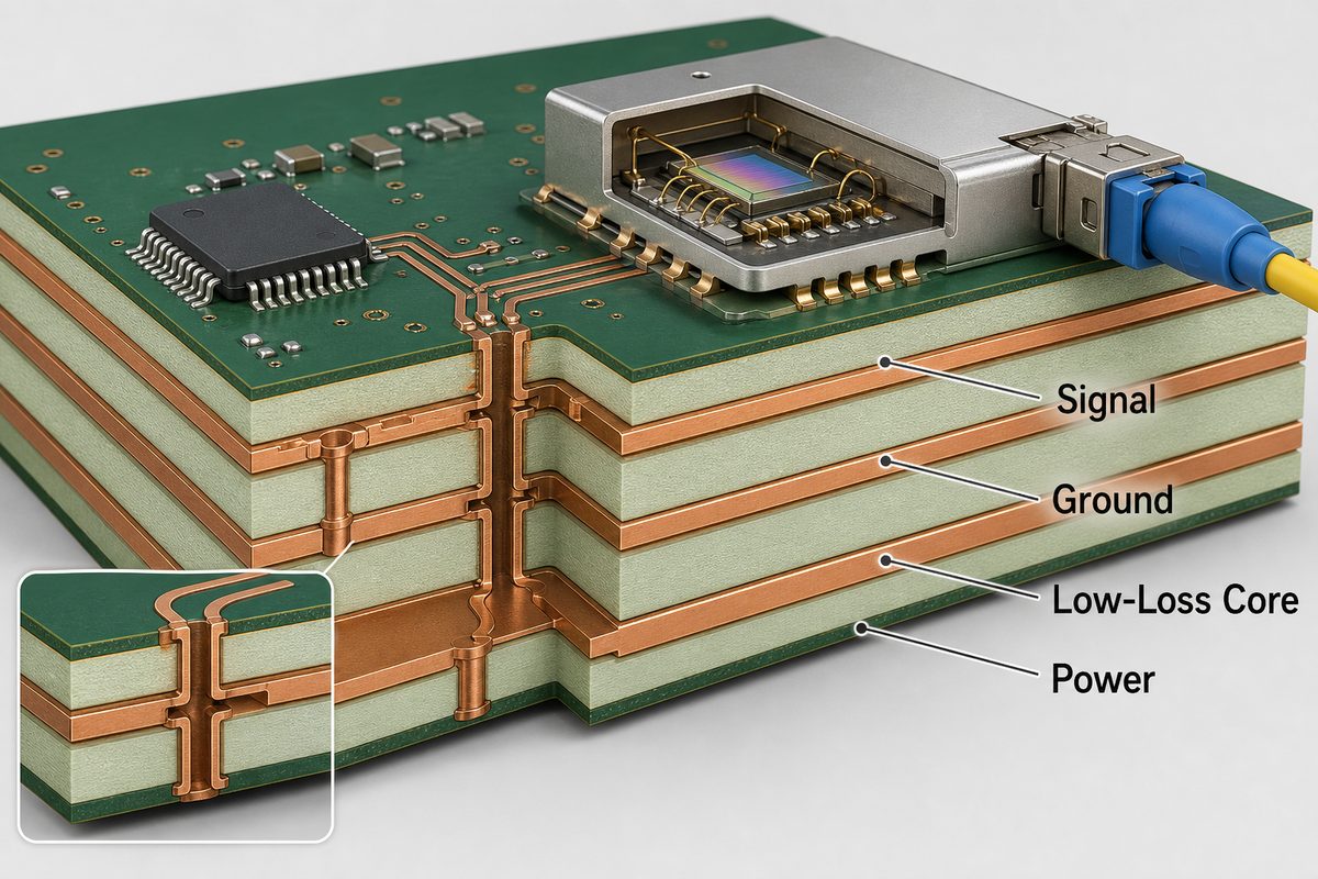
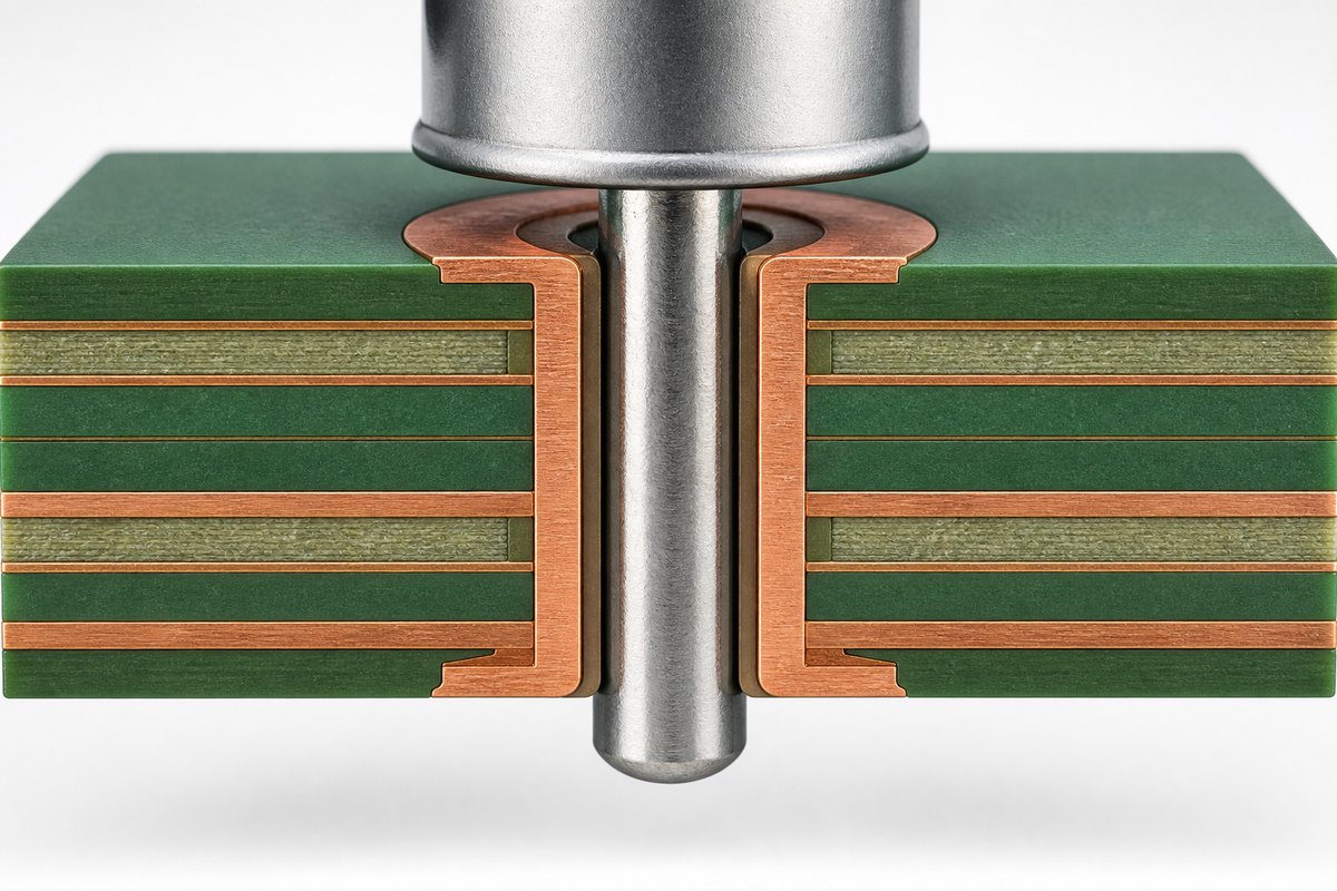
Cutaway view of an LPDA PCB showing the copper pattern, low-loss laminate, balanced feed, and SMA launch

How Should the Feed, Balun, and Connector Transition Be Designed?

The feed must preserve the intended balanced excitation while presenting the required impedance to the external cable or RF circuit. A coaxial connector is unbalanced, while the dipole array is balanced, so the transition should be treated as an RF structure rather than a simple pad connection.

Depending on the topology, the design may use a balanced parallel-strip feed, a microstrip-to-balanced transition, a tapered balun, a coplanar transition, or another simulated structure. The connector body and launch pads should be included in the model. A mathematically correct array can still show poor S11 if the launch adds excess inductance, capacitance, asymmetry, or unwanted common-mode current.

Log Periodic PCB Directional Antenna

A log periodic pcb directional antenna typically produces an end-fire beam toward its shorter elements, with the larger elements behind the active region. This direction should be confirmed in the radiation-pattern result rather than inferred only from the board outline.

LPDA is not automatically the best wideband PCB antenna for every enclosure. A Yagi may be simpler for a narrower band, while a Vivaldi antenna can provide another planar wideband path. The decision depends on band ratio, available length and width, polarization, gain flatness, front-to-back requirement, feed integration, and the surrounding structure.

Antenna Type Bandwidth Tendency Primary PCB Trade-Off
Printed LPDA Wide when the scale, feed, and truncation are optimized Long tapered array with many tolerance-sensitive cells
Printed Yagi Narrower and more frequency-specific Simpler element set but less suitable for a large band ratio
Vivaldi Wideband tapered-slot behavior Needs flare area and a carefully designed feed transition

Log Periodic PCB Antenna Calculator

A log periodic pcb antenna calculator is useful for generating the first set of element lengths, spacings, and array dimensions. It should not be treated as the final authority for a printed design because many calculators are based on simplified wire-LPDA relationships.

After the initial calculation, transfer the geometry into a full-wave solver with the real substrate, copper thickness, feed, connector, solder mask decision, and mechanical surroundings. Sweep both electrical and manufacturing variables. A design that works only at nominal geometry may drift after ordinary etching, material, or registration variation.

  • Document the calculator equations and the direction in which elements are indexed.
  • Keep the original target band separate from the wider simulation sweep.
  • Run sensitivity studies for Dk, dielectric thickness, copper width, and feed gap.
  • Export dimensioned fabrication data; do not ask the factory to recreate RF geometry from a screenshot.

Which Fabrication Tolerances Can Shift RF Performance?

The most sensitive fabrication variables are the ones that change resonant length, coupling, or feed impedance. On a wideband array, a small error repeated across many elements can alter gain flatness or create a local mismatch even when the board passes continuity testing.

  • Etch variation: changes arm width, arm length, feed width, and the gaps between conductors.
  • Dielectric variation: changes electrical length and feed impedance.
  • Layer registration: matters when alternate arms or balanced conductors occupy opposite sides.
  • Board outline and connector position: affect the launch and the mechanical reference.
  • Solder mask and surface finish: can add dielectric loading or change the conductor surface.
  • Handling and mounting: can bend a long thin board or bring metal hardware into the near field.

Controlled impedance is relevant to the feed, but it does not certify the antenna pattern. Review the feed geometry with the same discipline used for a radio frequency PCB, then keep the radiating elements under their own dimensional controls.

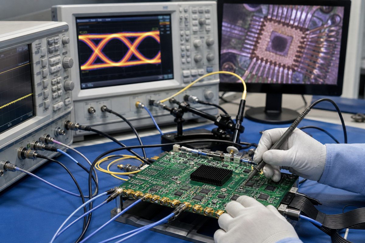
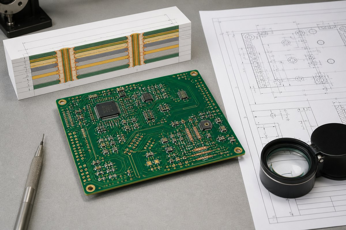
Optical dimensional inspection of copper elements on a printed LPDA antenna PCB

How Should a Fabricated LPDA PCB Be Tested?

A fabricated LPDA should be checked in stages: dimensional inspection first, port matching next, and radiation performance last. These tests answer different questions and should not be collapsed into a single pass/fail statement.

  1. Inspect the bare PCB: verify critical lengths, widths, gaps, registration, outline, connector position, and visible defects.
  2. Prepare the RF fixture: use the intended connector and mounting condition, then calibrate the VNA to a defined reference plane.
  3. Measure S11 or return loss: sweep beyond the target band to see edge behavior and unexpected resonances.
  4. Measure radiation performance: verify pattern direction, gain, beamwidth, front-to-back behavior, polarization, and efficiency when those are acceptance requirements.
  5. Compare samples: separate design error from fabrication variation by reviewing geometry and material records with the RF results.

A bare-board electrical test can find opens and shorts, but it cannot prove antenna gain or radiation pattern. Likewise, a good S11 trace does not guarantee that accepted power is radiated in the intended direction. The test plan must match the product’s actual RF acceptance criteria.

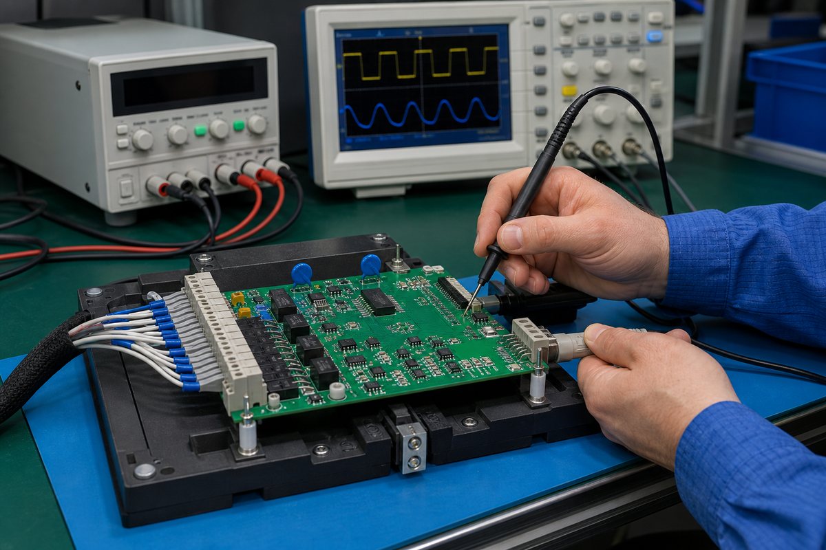
RF engineer measuring a printed LPDA antenna PCB with a vector network analyzer

What Data Should Be Included in an LPDA PCB Fabrication Package?

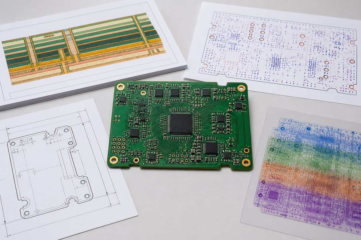
The fabrication package should define every board variable that the RF model assumes. Gerber or ODB++ data alone may show the artwork, but it may not explain the material values, controlled dimensions, connector reference, or acceptance method.

  • Gerber or ODB++ data, drill files, and a dimensioned drawing.
  • Exact laminate grade, finished dielectric thickness, and copper construction.
  • Critical finished dimensions and tolerances for elements, feed, and gaps.
  • Layer order, polarity, and registration requirements for balanced structures.
  • Surface finish and solder mask clearance instructions.
  • Connector part number, launch drawing, and board-edge requirements.
  • Target band, reference impedance, and available simulation or acceptance data.
  • Prototype quantity, production quantity, panel constraints, and assembly scope.

If the design uses a specific low-loss laminate, review its availability and processing route before freezing the stackup. The Rogers RO3010 material guide shows why material grade and dielectric data must be explicit in compact RF structures.

FAQ About Log Periodic Dipole Array Antenna PCBs

Is every printed LPDA automatically wideband?
No. The log-periodic geometry supports wideband behavior, but the useful band also depends on truncation, the feed transition, substrate, connector, material loss, nearby structures, and the acceptance metric.

Can FR4 be used for a printed LPDA?
Yes, if simulation and measurement show that its loss and dielectric variation are acceptable for the target band, board size, gain, and repeatability. A low-loss laminate may be safer when those margins are tight.

Does the longest dipole set the lower frequency limit?
It strongly influences the low-frequency edge, but the final limit also depends on dielectric loading, element width, spacing, feed behavior, and truncation margin. Do not size it from free-space half wavelength alone.

Which direction does an LPDA antenna radiate?
A conventional LPDA normally points toward its shorter elements. Confirm the actual main-beam direction in the simulated and measured pattern because feed and mechanical details can change the result.

Can PCB inspection replace antenna testing?
No. Dimensional inspection and electrical testing verify the board, while VNA and radiation measurements verify RF behavior. Both are needed when the antenna has formal performance requirements.

How Can EBest Circuit Support Your LPDA Antenna PCB?

At EBest Circuit, we support RF and high-frequency PCB projects with material and stackup review, controlled-impedance fabrication, prototypes, production orders, PCB assembly, and inspection. For an LPDA project, we can review the manufacturing data and identify board-level details that need clearer tolerances before production; final antenna performance remains tied to your validated RF design and test plan.

Send your Gerber or ODB++ files, stackup, laminate grade, target frequency band, connector drawing, critical tolerances, quantity, and available RF acceptance data to sales@bestpcbs.com. We will review the Log Periodic Dipole Array Antenna PCB fabrication requirements and prepare the appropriate PCB or PCBA quotation.

You may also like

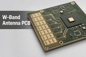
W-Band Antenna PCB: Design, Materials, Testing and Manufacturing

August 19th, 2026

A W-band antenna PCB integrates, feeds, packages or interconnects an antenna system operating in the W-band, commonly treated as 75-110 GHz. At these frequencies, laminate behavior, copper geometry, registration, transitions, assembly and test fixtures can change electrical performance, so the board must be designed and manufactured as part of the RF system rather than as a conventional interconnect.

The right implementation may be an etched antenna, a phased array, a substrate-integrated waveguide (SIW) structure, an antenna-in-package interface or a hybrid PCB-to-waveguide assembly. There is no universal stackup or trace dimension for every project. Electrical models, mechanical interfaces, fabrication limits and validation methods must be agreed for the actual design.

Realistic W-band antenna PCB with integrated array and RF feed structures

What Is a W-Band Antenna PCB?

A W-band antenna PCB is a frequency-sensitive circuit structure in which the board participates directly in radiation, RF feeding, beamforming, packaging or transition to another transmission medium. Small dimensional changes that are harmless at lower frequencies can create measurable phase, loss or impedance differences in W-band channels.

The term does not describe one fixed antenna shape. A PCB can carry a single radiating element, a corporate-feed network, a multi-channel array, SIW cavities, launch structures or the interface between a chipset and a waveguide antenna. A practical “mmwave pcb antenna” design therefore begins by defining which electromagnetic functions belong to the PCB and which belong to the package, connector, waveguide or surrounding enclosure.

W-band projects usually require closer coordination among antenna designers, package engineers, PCB fabricators, assemblers and test engineers. Their models must use compatible material assumptions, reference planes and mechanical dimensions; otherwise a board can meet its drawing yet miss the system target.

Where Are W-Band Antenna PCBs Commonly Used?

W-band antenna PCBs are used where compact antennas, short wavelengths, wide available bandwidth or fine angular resolution justify the added design and validation effort. The exact frequency allocation and product rules depend on the application and region, so the system specification should define the intended operating window.

Common engineering contexts include:

  • short-range and multi-gigabit wireless links;
  • imaging, sensing and research instruments;
  • phased-array and beam-steering platforms;
  • radar development above conventional automotive radar bands;
  • frequency-extender, calibration and laboratory evaluation hardware;
  • compact modules that transition between silicon, PCB and waveguide structures.

Which W-Band Antenna Type Is Best for Your PCB Project?

The best antenna type is the one that meets the radiation, bandwidth, packaging and manufacturing targets with a testable interface. A simple etched structure may reduce part count, while an array, SIW or antenna-in-package approach can better support gain, integration or feed control at the cost of added process sensitivity.

Architecture Typical fit Main manufacturing concern
Etched patch or slot Compact single element or small array Etch geometry, copper profile, dielectric thickness and surrounding metal
Corporate-fed array Higher gain or controlled beam pattern Feed symmetry, cumulative phase error and registration across channels
SIW or PCB waveguide Low-profile guided structures and transitions Via placement, cavity dimensions, plating and launch repeatability
Antenna-in-package Short chip-to-antenna path and dense integration Package-to-board transition, assembly alignment and warpage
Hybrid PCB-to-waveguide System connection to horn or metal waveguide Mechanical datum, aperture alignment, surface contact and fixture repeatability

A “w band patch antenna” can be suitable when its bandwidth, gain and installation environment are compatible with a planar radiator. A “w-band antenna array” is more appropriate when the system needs higher effective aperture or beam steering, but the additional channels make material variation, conductor geometry and assembly alignment harder to control.

What Should Be Confirmed Before W-Band Antenna PCB Design?

Confirm the RF, mechanical, material and validation boundaries before committing the layout. The project should not begin with a generic 50-ohm trace assumption because the usable geometry depends on the transmission structure, laminate construction, copper profile and surrounding reference planes.

The design team should establish:

  • operating frequency range, channel plan and required bandwidth;
  • antenna architecture, polarization, gain and scan requirements;
  • chipset, package, connector, waveguide and enclosure interfaces;
  • material family, target dielectric properties and allowed construction options;
  • stackup, copper profile, conductor definition and registration assumptions;
  • simulation reference planes and de-embedding approach;
  • acceptable amplitude, phase, impedance and radiation-pattern criteria;
  • prototype quantity, assembly state and planned validation stages.

These inputs do not need to become a long document checklist. They need to be consistent. A model based on one dielectric thickness or copper treatment cannot reliably predict a board manufactured with another construction.

How Should a W-Band Antenna Be Placed and Routed on the PCB?

Place the antenna and its feed network as a controlled electromagnetic region, not as ordinary signal routing. Keep the layout consistent with the simulated stackup, reference planes, enclosure and launch geometry, and protect the antenna aperture from copper, components and mechanical features that were absent from the model.

Useful layout controls include:

  • keeping feed paths short, geometrically consistent and free of unplanned neck-downs;
  • preserving the intended ground return and avoiding reference-plane discontinuities;
  • using symmetric routing where array channels require matched phase and amplitude;
  • locating via fences and SIW rows from the electromagnetic design, not from a generic spacing rule;
  • defining copper keepouts around radiating elements and transitions;
  • placing mounting holes, shields, fasteners and enclosure walls in the simulation model;
  • avoiding solder mask or surface treatments over critical RF regions unless the design explicitly includes them.

Via stitching can support ground continuity and field confinement, but more vias are not automatically better. Via diameter, pitch, antipad, plating and distance from the RF structure all affect the local field and manufacturability.

Which Materials and Stackups Affect W-Band Antenna Performance?

Materials and stackups affect W-band performance through dielectric constant, loss, thickness variation, moisture behavior, copper roughness, glass weave and construction repeatability. A material name alone is not enough; the design model should reflect the actual laminate, copper and fabrication construction being purchased.

Cutaway view of multilayer W-band antenna PCB materials, copper layers and via structures

Review these variables together:

  • design Dk and its test method at a relevant frequency;
  • dissipation factor and conductor-loss assumptions;
  • dielectric thickness and its manufacturing tolerance;
  • copper foil type, profile and plated thickness;
  • glass reinforcement or anisotropy when present;
  • bondply, prepreg or adhesive behavior in a hybrid stackup;
  • dimensional stability through lamination and subsequent thermal cycles;
  • surface finish and solder mask interaction with exposed RF conductors.

Low nominal Df does not guarantee low insertion loss if rough copper, long feeds or poor transitions dominate. Likewise, two laminate constructions with similar datasheet Dk values may produce different effective impedance and phase when their reinforcement, resin content or copper profile differs. For a broader material context, see our RF Microwave PCB guide.

How Do Feed Lines, Impedance Matching, Vias and Transitions Affect Performance?

Feed lines and transitions determine how much of the generated W-band energy reaches the antenna with the intended amplitude and phase. The whole path must be modeled across launches, vias, package pads, cavities, connectors and waveguide interfaces; checking only a straight transmission-line coupon leaves the most sensitive discontinuities untested.

At W-band, a transition can add loss or resonance through a small pad, antipad, stub, air gap or registration shift. Channel-to-channel differences can also accumulate through small length and geometry variations. The design should therefore define the reference plane for every reported result and distinguish simulated antenna impedance from the impedance seen through the complete feed and fixture.

Impedance control PCB principles still apply, but a conventional coupon may not represent the antenna feed, via transition or package launch. Use dedicated test structures when the project needs to separate material, line, transition and fixture effects.

What Is the W-Band Antenna PCB Design and Manufacturing Process?

The process should connect electromagnetic design, fabrication engineering and staged verification so that production data preserve the modeled structure. The PCB fabricator should review the stackup and critical geometry before release, while the antenna designer retains responsibility for RF synthesis and system-level performance.

Engineer inspecting a high-frequency antenna PCB under an optical measurement microscope
  1. Define the operating band, antenna architecture, interfaces and validation targets.
  2. Select a manufacturable material system and build the preliminary stackup.
  3. Simulate the antenna, feed network, transitions, package and nearby mechanical features.
  4. Add fabrication tolerances to sensitivity analysis instead of validating only nominal geometry.
  5. Complete PCB DFM review for conductor definition, registration, drilling, plating and lamination.
  6. Fabricate coupons or representative test structures with the prototype panel.
  7. Inspect the bare board before assembly and record actual stackup or dimensional results where required.
  8. Assemble with controlled alignment, reflow profile, flatness and handling conditions.
  9. Measure interconnect behavior and antenna performance using agreed reference planes.
  10. Correlate test results with the model before freezing the production build.

A useful “mmwave pcb design guide” must include this feedback loop. If the prototype fails, the team needs enough coupon, dimensional and fixture data to identify whether the cause is the antenna model, the feed path, fabrication variation, assembly or measurement setup.

Why Does a W-Band Antenna PCB Show High Loss, Weak Gain or Phase Error?

High loss, weak gain and phase error usually come from several interacting sources rather than one obvious defect. Diagnose the signal path in stages and compare nominally identical channels before changing the antenna geometry.

Symptom Likely cause group First check
Higher insertion loss Material loss, copper roughness, long feed or transition loss Compare line and transition test structures before OTA testing
Resonance shifted Dielectric thickness, effective Dk, etch geometry or nearby metal Measure critical dimensions and confirm the built stackup
Weak or distorted pattern Feed imbalance, enclosure interaction, assembly obstruction or fixture scattering Repeat with the agreed mechanical configuration and calibration boundary
Channel phase spread Line-length, weave, copper, registration or package variation Compare matched channels through the same fixture and reference plane
Poor repeatability Connector torque, waveguide alignment, contact, cable movement or calibration drift Re-seat the fixture and run a repeatability study

Do not tune the board from a single unverified measurement. First confirm calibration, fixture repeatability and reference-plane location. Then compare bare-board dimensions, material construction and assembly state against the model.

How Should a W-Band Antenna PCB Be Tested Before Production?

Test a W-band antenna PCB in layers: bare-board quality, RF interconnect behavior and over-the-air antenna performance answer different questions. A PCB supplier can verify fabrication features and agreed electrical structures, but antenna gain and radiation pattern require suitable W-band equipment, fixtures and an OTA method.

W-band antenna PCB mounted in a millimeter-wave laboratory test fixture

A practical validation sequence may include:

  • visual and dimensional inspection of critical conductors, apertures and registration;
  • microsection or construction verification for selected vias and layer relationships;
  • continuity, isolation and agreed impedance or transmission-line coupons;
  • line and transition measurements with defined calibration and de-embedding;
  • channel-to-channel amplitude and phase comparison for arrays;
  • assembled-module checks with the final package, connector or waveguide interface;
  • OTA return loss, gain, pattern, polarization and scan testing when the responsible laboratory capability is confirmed.

W-band characterization commonly uses frequency extenders and waveguide hardware. Fixture design, flange alignment and calibration boundaries must be documented because a fixture error can look like a PCB or antenna defect.

How Do Assembly and Packaging Affect W-Band Antenna Performance?

Assembly and packaging affect W-band performance by changing alignment, standoff, flatness, local dielectric loading and transition geometry. A bare board that matches its drawing can still perform differently after a chipset, shield, radome, heat spreader or waveguide block is installed.

Control the assembly variables that are included in the RF model:

  • package placement and rotation relative to feed structures;
  • solder volume, collapse and standoff for flip-chip or fine-pitch interfaces;
  • board and package warpage through reflow;
  • underfill, adhesive or coating near active RF regions;
  • connector or waveguide flange alignment and fastener sequence;
  • shield, enclosure and absorber position;
  • cleanliness and surface contamination around exposed conductors.

If assembly is outsourced separately from PCB fabrication, provide the assembler with the RF-sensitive keepouts and mechanical datums. Standard placement tolerances may not describe the relative alignment that the antenna transition actually needs.

What Factors Affect W-Band Antenna PCB Cost?

W-band antenna PCB cost is driven by material choice, stackup complexity, tolerance control, prototype learning and validation—not by board area alone. Early agreement on which characteristics are truly critical can prevent unnecessary controls while protecting RF performance.

The main cost drivers are:

  • specialty laminate availability and minimum purchase quantities;
  • hybrid or sequential lamination construction;
  • thin dielectric layers and tight thickness control;
  • fine conductor geometry, copper-profile requirements and etch compensation;
  • registration demands across antenna, feed and via structures;
  • small or dense plated holes, SIW rows and backdrilling when applicable;
  • dedicated coupons, dimensional reports, microsections or RF test structures;
  • assembly alignment, package complexity and special fixtures;
  • prototype iterations needed to correlate simulation and measured results;
  • production quantity, panel utilization and accepted yield window.

Cost should be reviewed against the validation plan. Removing a useful test structure may reduce initial panel cost but make a failed prototype harder to diagnose. Conversely, specifying a universal tight tolerance without sensitivity evidence can add cost without improving the antenna.

FAQ About W-Band Antenna PCB Projects

Is W-band always defined as 75-110 GHz?

75-110 GHz is a common engineering definition for the W-band, but applications, instruments and regulations may use narrower windows. State the exact operating range and channel plan in the project specification rather than relying only on the band name.

Can a w band patch antenna be fabricated as a conventional multilayer PCB?

It can use familiar PCB processes, but the construction may need tighter control of dielectric thickness, copper geometry, surface condition and registration than a conventional digital board. The antenna model must use the proposed stackup and manufacturing tolerances.

Which laminate properties matter most for a mmwave pcb antenna?

Design Dk, dissipation factor, thickness tolerance, copper roughness, reinforcement structure, moisture behavior and dimensional stability can all matter. Their relative importance depends on whether loss, phase consistency, resonance or mechanical stability dominates the design.

Does a PCB supplier validate antenna gain and radiation pattern?

Not automatically. A PCB supplier may inspect construction, dimensions and agreed RF coupons. Gain, radiation pattern, polarization and scan performance require suitable W-band fixtures and OTA equipment, so the responsible test party and acceptance method must be confirmed for each project.

What project information should be confirmed before production?

Confirm the operating range, antenna type, final stackup, named laminate, copper construction, critical geometry, mechanical interfaces, assembly state, quantity and acceptance method. Provide Gerber or ODB++ data plus relevant package or waveguide drawings when they are part of the manufactured interface.

Why can nominally identical antenna channels show different phase or gain?

Small differences in feed length, dielectric construction, glass weave, copper profile, registration, package alignment or fixture contact can accumulate across channels. Compare the channels through the same calibrated setup and inspect actual geometry before changing the design.

How Can EBest Circuit Support Your W-Band Antenna PCB Project?

EBest Circuit supports RF and high-frequency PCB manufacturing, impedance-controlled PCB work, impedance testing and engineering review for available high-frequency material systems. Because W-band performance depends on the exact stackup, copper construction, antenna topology, transitions and validation method, we review each design for manufacturability and sourcing feasibility rather than promise one universal process window.

Send the target frequency range, antenna architecture, Gerber or ODB++ data, stackup, material and copper requirements, critical tolerances, package or waveguide interface drawings, assembly information, quantity and RF acceptance plan to our engineering team at sales@bestpcbs.com. We can review the PCB manufacturing and assembly scope with your team. Antenna synthesis, W-band VNA measurement and OTA gain or pattern validation are included only when the responsible capability is confirmed for the specific project.

You may also like

20 Layer PCB: Stackup, Thickness, Design & Manufacturing Guide

August 18th, 2026

A 20 layer PCB is usually chosen when a design needs more routing channels, reference planes, or power distribution than a lower-layer board can comfortably provide. High-pin-count BGAs, fast digital interfaces, multiple voltage rails, limited board area, and strict EMI requirements are common reasons to move toward this type of construction. The extra layers offer more design freedom, but they also make stackup planning, drilling, lamination, and registration more demanding.

EBest Circuit manufactures multilayer PCBs and supports engineering review for stackup, controlled impedance, via structures, materials, and DFM. If your design is already at the 16- to 20-layer stage, sending the Gerber or ODB++ data together with target thickness, copper weight, impedance requirements, and drill information allows the board construction to be reviewed before quotation or prototype release.

20 layer PCB showing multilayer stackup, copper layers and plated vias

What Is a 20 Layer PCB?

A 20 layer PCB uses twenty copper layers to combine dense routing, reference planes, power distribution, and controlled-impedance structures in one multilayer board. It is appropriate only when the design needs the extra routing and plane flexibility.

A practical stackup normally combines:

A 20 layer board should be selected from routing, power, EMI, and mechanical requirements rather than layer count alone.

  • Signal layers for component breakout and routing
  • Ground planes for return paths and shielding
  • Power planes for voltage distribution
  • Reference planes for controlled-impedance signals

The advantage is not simply “more layers.” What matters is how those layers are allocated. A good 20-layer construction can give high-speed traces nearby reference planes, keep return paths continuous, and provide enough routing space without pushing trace width and spacing unnecessarily tight.

When Do You Need a 20 Layer PCB?

A 20-layer structure makes sense when a lower layer count starts forcing electrical or routing compromises.

Typical cases include:

  • High-pin-count BGA, CPU, FPGA, or ASIC breakout
  • Multiple DDR, PCIe, Ethernet, SerDes, USB, or other high-speed interfaces
  • Several power rails requiring dedicated plane area
  • Dense layouts where board size cannot increase
  • Mixed analog, digital, RF, and power circuitry
  • Designs requiring additional ground planes for EMI control
  • Backplanes, servers, telecom equipment, medical electronics, aerospace systems, and complex industrial controls

More layers are not automatically better. If a 16-layer board already meets routing, signal-integrity, power-integrity, and mechanical requirements with reasonable margin, moving to 20 layers only adds fabrication complexity and cost.

What Does a Typical 20 Layer PCB Stackup Look Like?

There is no universal 20 layer PCB stackup. Layer allocation depends on BGA escape, impedance requirements, dielectric thickness, copper weight, power distribution, and the intended via structure.

This pcb layer stack up example is illustrative; the production construction must be recalculated for the approved materials and impedance targets. See our PCB board stackup guide.

20 layer PCB stackup example with signal ground and power layers

A possible 20 layer PCB stackup example is shown below.

Layer Type Typical Function
L1 Signal Components and short routing
L2 Ground Reference plane
L3 Signal High-speed routing
L4 Ground Reference plane
L5 Signal General routing
L6 Power Power distribution
L7 Signal General/high-speed routing
L8 Ground Reference plane
L9 Signal High-speed routing
L10 Ground Central reference plane
L11 Ground Central reference plane
L12 Signal High-speed routing
L13 Ground Reference plane
L14 Signal General/high-speed routing
L15 Power Power distribution
L16 Signal General routing
L17 Ground Reference plane
L18 Signal High-speed routing
L19 Ground Reference plane
L20 Signal Components and routing

This is an example, not a standard construction. A real project may need more power layers, fewer signal layers, different dielectric spacing, or another reference-plane arrangement. The stackup should be finalized against the actual impedance and manufacturing requirements rather than copied from another PCB.

How Should Signal, Ground, and Power Layers Be Arranged?

Layer placement should give critical signals a stable reference and keep the overall construction reasonably symmetrical.

Several rules are especially useful:

  • Place high-speed signal layers next to continuous ground planes.
  • Avoid routing critical traces across gaps or splits in their reference plane.
  • Use ground layers between sensitive or unrelated routing regions when isolation is important.
  • Keep power and ground planes appropriately coupled where the stackup allows.
  • Maintain a reasonably symmetrical dielectric and copper structure around the board center.
  • Avoid large copper-density differences between opposite sides of the stack.

Return-path planning is particularly important. When a high-speed signal changes layers, the return current must also transition between reference planes. If both references are ground, nearby stitching vias can provide a short return path.

Layer assignment is best decided before detailed routing. Changing the stackup late in the design can alter impedance geometry and force trace-width or spacing changes.

What Is the Typical 20 Layer PCB Thickness?

There is no single standard 20 layer PCB thickness. The finished value comes from the complete copper and dielectric build rather than the layer count by itself.

20 layer PCB thickness measured across copper core and prepreg layers

Finished thickness is mainly determined by:

  • Core thickness
  • Cured prepreg thickness
  • Copper weight
  • Required finished copper
  • Controlled-impedance geometry
  • Electrical isolation requirements
  • Via diameter and drill aspect ratio
  • Connector and enclosure requirements
  • Mechanical stiffness

Trying to make a 20-layer board unusually thin means using thinner dielectric layers. That can affect impedance geometry, laminate availability, registration tolerance, and mechanical strength.

Board thickness also needs to be reviewed with the drill table. A thick PCB combined with very small mechanically drilled holes can create an aggressive aspect ratio, making hole preparation and plating more difficult. For this reason, thickness, stackup, impedance, and hole structure should be evaluated together.

Which Materials Are Used for 20 Layer PCBs?

Layer count alone does not determine the laminate. Material selection should follow the electrical, thermal, reliability, and cost requirements.

Our PCB material guide explains how Tg, loss, and laminate construction affect selection.

20 layer PCB materials including FR-4 high Tg low loss RF and hybrid laminates
Material Type Typical Use Main Consideration
Standard FR-4 General industrial electronics Economical for less demanding signal speeds
High-Tg FR-4 Dense boards with higher thermal demands Better thermal robustness
Low-loss laminate High-speed digital systems Lower transmission loss
RF/high-frequency laminate RF and microwave sections More stable Dk and lower Df
Hybrid stackup Mixed digital/RF designs Lamination compatibility needs review

For high-speed boards, two material properties deserve particular attention:

  • Dk influences impedance and propagation delay.
  • Df contributes to dielectric loss, especially as frequency and trace length increase.

Availability also matters. A laminate may look ideal electrically but become impractical if the required core or prepreg thickness is difficult to source for prototypes or volume production. Hybrid constructions need closer review because different material systems may have different resin behavior, CTE, and lamination conditions.

How Do You Design a 20 Layer PCB for Signal and Power Integrity?

More layers make SI and PI design easier only when they are used correctly.

For manufacturing controls, review our impedance control PCB guide.

For controlled impedance, the PCB manufacturer needs more than the requested value. Actual impedance depends on:

  • Trace width
  • Copper thickness
  • Dielectric thickness
  • Dk
  • Distance to the reference plane
  • Differential-pair spacing
  • Manufacturing tolerance

The production impedance calculation should therefore use the actual fabrication stackup rather than nominal CAD dimensions alone.

Other practical design points include:

  • Keep high-speed traces over continuous reference planes.
  • Avoid unnecessary layer changes on sensitive interfaces.
  • Add suitable return-path vias when reference planes change.
  • Control coupling between neighboring high-speed routes.
  • Review via stubs on faster channels.
  • Keep decoupling paths short between the power pin, capacitor, and ground.
  • Allocate sufficient copper for major power rails.

Via stubs can become important at higher data rates. If a through via continues well beyond the layers carrying the signal, the unused section acts as a stub. Back drilling or a shorter blind-via transition may be considered when channel analysis shows the stub is significant.

The objective is not to fill the stackup with ground and power planes. It is to create enough routing space while maintaining clean reference paths and a low-impedance power-distribution network.

Which Via Structures Are Suitable for a 20 Layer PCB?

A 20 layer PCB does not automatically need HDI construction. The appropriate via type depends mainly on package pitch, routing density, board thickness, and the layers that must be connected.

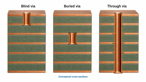
Through blind buried microvia and via in pad structures for a 20 layer PCB
Via Type Suitable Situation Main Trade-Off
Through via Moderate routing density Occupies space through the full stack
Blind via Dense outer-layer breakout More process steps
Buried via Internal layer connections More complex lamination
Microvia Fine-pitch BGA or HDI routing Often requires sequential lamination
Via-in-pad Very dense BGA escape Filling and planarization usually required
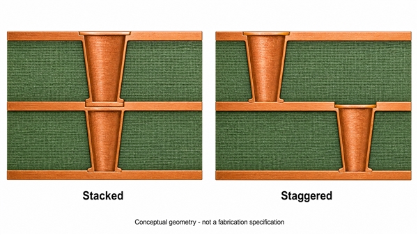
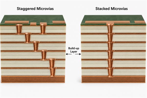
Staggered microvia Multi-level HDI routing More layout planning
Stacked microvia Vertical HDI interconnect Tighter process and reliability control

For example, a 20-layer industrial controller with generous component pitch may work well with conventional through vias. A much smaller board using fine-pitch BGAs may require microvias even at the same layer count.

Layer count and HDI level are separate design decisions.

How Is a 20 Layer PCB Manufactured?

The basic process is similar to other multilayer PCBs, but dimensional control becomes more important as the stack grows.

A typical manufacturing flow includes:

  1. Inner-layer imaging and etching
  2. Inner-layer AOI
  3. Surface preparation
  4. Core and prepreg layup
  5. Multilayer lamination
  6. Mechanical or laser drilling
  7. Hole metallization and copper plating
  8. Outer-layer imaging and etching
  9. Solder mask
  10. Surface finish
  11. Electrical testing
  12. Final inspection

A conventional through-hole board may use one main multilayer lamination cycle. Designs with buried vias or multi-level microvias can require repeated lamination, drilling, and plating.

That difference can have a major effect on cost and lead time. A “20-layer PCB” therefore tells the manufacturer much less than a complete stackup and via diagram.

What Are the Key Manufacturing Challenges of a 20 Layer PCB?

The main challenge is controlling many interacting tolerances at the same time.

Important DFM points include:

  • Layer registration: inner layers can expand or contract during processing, so registration compensation is required.
  • Drill aspect ratio: small holes through a thick board are more difficult to prepare and plate reliably.
  • Resin flow: uneven copper distribution can affect dielectric thickness and resin fill.
  • Copper balance: severe imbalance may contribute to bow and twist.
  • Hole-wall plating: plating must remain continuous through the full hole depth.
  • CAF risk: conductor and hole spacing, material selection, and process control deserve attention on dense multilayer designs.
  • Delamination: laminate condition, moisture control, pressing, and thermal exposure all matter.
  • Impedance consistency: dielectric and copper tolerances need to stay within the range used for the impedance calculation.

A useful DFM review should therefore examine the real stackup, drill map, copper distribution, via construction, impedance table, and material specification—not just confirm that the factory can produce “20 layers.”

20 Layer PCB vs 16 Layer PCB: Which Should You Choose?

A 20-layer board provides more routing and plane-allocation freedom, while a 16-layer structure is generally simpler to manufacture.

Comparison of 20 layer PCB and 16 layer PCB routing and stackup complexity
Factor 16 Layer PCB 20 Layer PCB
Routing capacity High Higher
Reference-plane flexibility Good Greater
Power-plane allocation Good More flexible
Dense BGA routing Suitable for many designs Better for highly congested designs
Stackup complexity Lower Higher
Fabrication cost Lower Higher
Manufacturing difficulty Lower Higher

Consider moving from 16 to 20 layers when the 16-layer design causes:

  • Excessive routing congestion
  • Too many signal layer transitions
  • Broken or compromised reference planes
  • Inadequate BGA escape channels
  • Insufficient room for power planes
  • Trace spacing that is unnecessarily aggressive

If those problems do not exist, 16 layers may be the more economical choice.

What Affects 20 Layer PCB Cost and Lead Time?

Layer count matters, but two 20-layer designs can still have very different prices.

The largest quotation variables usually include:

  • Board dimensions and panel utilization
  • Laminate type and availability
  • Finished thickness
  • Copper weight
  • Minimum trace and spacing
  • Minimum finished hole size
  • Blind, buried, or microvia structures
  • Number of sequential lamination cycles
  • Via filling or via-in-pad
  • Controlled impedance
  • Back drilling
  • Surface finish
  • Testing requirements
  • Prototype or production quantity

A conventional FR-4 board using through vias is generally less complex than a 20-layer low-loss design with stacked microvias, back drilling, via filling, and tight impedance requirements.

For a meaningful quotation, provide the complete fabrication requirements rather than asking for a generic “20 layer PCB price.”

20 Layer PCB FAQ

How thick is a 20 layer PCB?

There is no fixed thickness. It depends on the core and prepreg structure, copper weight, controlled-impedance geometry, via structure, and mechanical requirements. If the finished thickness is mechanically constrained, specify it early so the stackup and drill aspect ratio can be evaluated together.

How many signal layers does a 20 layer PCB have?

There is no standard number. Some 20-layer boards may use around half of the layers for routing, while others allocate more copper layers to ground or power. The correct ratio depends on routing density, power distribution, and signal-integrity requirements.

Does a 20 layer PCB always require HDI technology?

No. A conventional through-hole construction can be suitable when component pitch and routing density allow it. HDI becomes useful when fine-pitch BGA breakout or limited PCB area requires blind vias, buried vias, or microvias.

Can a 20 layer PCB use standard FR-4?

Yes, when its loss, thermal, and reliability requirements are compatible with standard FR-4. High-speed interfaces, long transmission paths, or higher thermal demands may justify high-Tg or lower-loss laminates.

What files are required for a 20 layer PCB quote?

For an accurate review and quotation, provide as much of the following as available:

  • Gerber or ODB++ files
  • NC drill files
  • Fabrication drawing
  • Finished board thickness
  • Copper weight
  • Existing stackup
  • Controlled-impedance requirements
  • Via structure
  • Material preference
  • Surface finish
  • Quantity
  • Inspection or reliability requirements

A 20 layer PCB is most useful when the added layers solve real routing, reference-plane, power-distribution, or density problems. Stackup, thickness, material, impedance, and via architecture should be developed as one system rather than specified independently.

How Can EBest Circuit Support Your 20 Layer PCB Project?

A supplier’s published maximum layer count is only a starting point. What matters is whether its process capability matches your actual stackup.

Check whether the manufacturer can support:

  • Multilayer stackup engineering
  • Controlled-impedance calculation and verification
  • Required minimum trace, spacing, and hole geometry
  • Blind and buried vias
  • HDI and sequential lamination where required
  • Via filling and via-in-pad
  • Inner-layer AOI
  • Electrical testing
  • Cross-section inspection where needed
  • Material and production traceability
  • Relevant quality-system requirements
  • DFM review before fabrication

Engineering communication is also revealing. If a stackup, drill structure, or impedance requirement is unclear, the issue should be raised before production rather than interpreted silently.

For EBest Circuit projects, customers can provide Gerber or ODB++, drill files, fabrication notes, target thickness, impedance information, and material requirements for engineering review before prototype or volume production.

Send us your Gerber or ODB++ files, drill data, target thickness, material grade, copper weights, impedance targets, via structure, quantities, and test requirements. We can review stackup balance and manufacturability before quotation and prototype release.

You may also like

Router PCB Design, Prototyping and Manufacturing Services for Wi-Fi and Ethernet Products

August 17th, 2026

A router PCB must move data reliably while controlling RF coupling, power noise, heat and electromagnetic emissions inside a compact enclosure. EBest Circuit supports custom router PCB projects from engineering review and prototype fabrication through component assembly and repeat production. This guide explains the decisions that buyers and hardware teams should settle before requesting a quotation or releasing production data.

Router PCB design prototyping and manufacturing services for Wi-Fi and Ethernet products

Are you worried about delays or unexpected problems during router PCB design, prototyping and assembly?

  • Have the Ethernet, Wi-Fi, RF, power and return-path requirements been defined early enough to avoid late stackup changes and unnecessary board revisions?
  • Are the fabrication files, BOM and test criteria complete and aligned, or will missing details hold up the first build?
  • Can your manufacturing partner handle BGAs, RF components, connectors and approved substitutions while maintaining solder quality and consistent performance?

With 20 years of PCB and PCBA manufacturing experience, EBest Circuit supports router projects from design review through prototyping, assembly and production. Our one-stop service helps turn complex or incomplete requirements into a controlled, buildable manufacturing package.

  • Lock critical board requirements before fabrication: EBest reviews the proposed stackup, impedance table, Ethernet and RF reference routes, power-return paths, component footprints and DFM conflicts, then returns a clear issue list for customer confirmation.
  • Release one build-ready data package: EBest cross-checks Gerber or ODB++, drill data, the BOM, centroid files, drawings, firmware and measurable test limits so purchasing and production work from the same approved revision.
  • Control placement, soldering and verification: EBest confirms approved part numbers and substitutions, plans stencil and reflow requirements for BGAs and RF components, applies AOI and X-ray where appropriate, and checks agreed functions against documented acceptance criteria.

Ready to start your router PCB project? Send your design files, BOM, quantities and test requirements to sales@bestpcbs.com for an engineering review and quotation.

What Router PCB Design and Manufacturing Services Does Your Project Need?

The right service scope depends on how complete and proven your design is. A team with released Gerber files, a validated BOM and finished test software may need fabrication and assembly only. A project at schematic stage needs stackup planning, placement review, impedance definition, DFM feedback and a prototype test plan before production.

  • Design support: schematic review, component placement, stackup coordination, controlled-impedance planning and layout review.
  • PCB prototyping: small-batch fabrication for electrical, RF, thermal and enclosure validation.
  • PCB assembly: component sourcing, stencil preparation, SMT, through-hole assembly, rework and inspection.
  • Production support: panelization, test-fixture planning, traceability requirements and controlled engineering changes.

What Should Be Confirmed Before Starting a Router PCB Design?

Freeze the product interfaces and operating conditions before optimizing the board. The processor, Ethernet PHY, switch, memory, radio module or RF chipset, power architecture and antenna arrangement determine most routing and stackup decisions.

  • Network interfaces: record Ethernet speed, port count, magnetics arrangement, PoE requirement and connector choice.
  • Wireless functions: define Wi-Fi bands, MIMO channel count, antenna type, RF connector locations and coexistence requirements.
  • Mechanical limits: provide board outline, mounting holes, connector keepouts, enclosure height limits and airflow direction.
  • Power conditions: identify every input source, rail current, transient load, sequencing requirement and protection circuit.
  • Environment: state operating temperature, humidity, vibration, installation type and expected service life.

How Should Ethernet, Wi-Fi, RF and High-Speed Interfaces Be Laid Out on a Router PCB?

Each high-speed or RF interface needs a continuous return path and a routing rule based on its device documentation. Do not assign one generic trace width to Ethernet pairs, USB, memory and RF lines. Their target impedance, reference layer, loss budget and matching rules differ.

Router PCB RF and high-speed interface testing with oscilloscope probes

  • Ethernet pairs: keep each pair coupled, minimize skew, avoid plane splits and follow the PHY and magnetics reference layout for spacing and termination.
  • RF paths: keep transceiver-to-filter-to-antenna routes short, isolate them from switch nodes and crystals, and use the antenna vendor’s keepout rules.
  • Memory buses: place memory near the processor, control topology and length relationships, and avoid unnecessary layer transitions.
  • Reference transitions: add nearby return vias when a signal changes reference layers so the return current does not take a long detour.

How Do You Select the Stackup, Controlled Impedance and Materials for a Router PCB?

Select the stackup with the fabricator before final routing because dielectric thickness, copper weight and material properties set the impedance geometry. Layer count should provide practical signal layers, uninterrupted reference planes and adequate power distribution rather than simply meeting a board-thickness target.

For ordinary FR-4 multilayer work, EBest’s supplied capability table lists standard production from 1 to 10 layers, with high-Tg material required at eight layers and above; 10 to 32 layers require special evaluation. It lists standard 4/4 mil inner-layer line and spacing for 1/2 oz copper and standard 4/4 mil outer-layer line and spacing for 1 oz copper, with 3/3 mil treated as a special capability. These are manufacturing limits, not automatic design rules. A router PCB should use comfortable geometry wherever space permits.

Decision Confirm Before Layout Release Requirement
Layer stackup Layer order, dielectric thickness, copper weight and finished thickness Fabricator-approved stackup drawing
Controlled impedance Target, tolerance, trace type and reference plane Impedance table tied to net classes
Material Laminate family, Tg needs, loss needs and availability Approved material and substitution rule
Via structure Finished hole, aspect ratio and any blind or buried vias Drill table and fabrication notes

How Can You Control Signal Integrity, Power, Thermal and EMI Risks in Router Hardware?

Treat signal integrity, power integrity, heat and EMI as one coupled system. A noisy regulator can modulate a radio rail; poor return paths can increase emissions; excessive processor temperature can shift performance and shorten component life.

  • Power integrity: place decoupling capacitors at the intended device pins, keep high-current loops compact and verify rail droop during traffic bursts.
  • Thermal control: use thermal vias and copper spreading where appropriate, model enclosure airflow and measure component temperatures under sustained traffic.
  • EMI control: contain switching-current loops, preserve reference planes, separate sensitive RF areas and reserve practical shield-can boundaries when required.
  • Clock control: keep oscillators and clock routes away from antenna feeds, RF inputs and board edges; follow the clock source termination guidance.

What Files and Specifications Are Needed for Router PCB Prototyping?

A buildable prototype package must define the board, the assembly and the expected test result. Gerber or ODB++ data alone does not tell an assembler which component revision to buy or how to judge a programmed board.

  • Fabrication package: Gerber or ODB++, NC drill data, board outline, stackup, impedance table, fabrication drawing and readme.
  • Assembly package: BOM with manufacturer part numbers, centroid file, assembly drawings, polarity notes and approved substitutes.
  • Programming package: firmware image, programming tool requirements, connector or fixture definition and verification method.
  • Test package: power limits, expected rail values, interface checks, test-point map and pass/fail limits.

Cross-check revision identifiers before release. The fabrication drawing, Gerber or ODB++ data, BOM, centroid file, assembly drawing and firmware must all describe the same board revision. A shifted coordinate origin can misplace every component, an unapproved BOM alternative can change RF or power behavior, and a test instruction without measurable limits leaves the first build open to interpretation. Resolve these conflicts before material is ordered, then issue one dated package so purchasing, fabrication, assembly and test use the same baseline.

Which DFM Checks Should Be Completed Before Router PCB Fabrication?

DFM must check whether the released geometry can be fabricated, assembled and tested repeatedly. A basic clearance check is necessary but insufficient for a dense router board with BGAs, shields, fine-pitch RF parts and multiple external connectors.

  • Fabrication review: verify annular rings, drill-to-copper clearance, copper-to-edge spacing, solder-mask registration, aspect ratio and impedance coupons.
  • Assembly review: check paste apertures, BGA fan-out, component spacing, polarity visibility, shield-can access and rework clearance.
  • Panel review: confirm rail width, tooling holes, fiducials, breakaway strategy and connector overhang.
  • Test review: keep critical power, reset, programming and communication nodes accessible to probes or a fixture.

Classify each DFM finding by the action it requires. A copper clearance, annular-ring or solder-mask violation normally needs corrected production data; an impedance geometry question may require stackup confirmation and a revised trace rule; a connector overhang or shield-access issue may need mechanical approval. Record the affected layer, component or net, the proposed change and the person approving it. This prevents a fabricator’s local edit from becoming an undocumented design revision and makes the corrected package traceable for the next build.

What Does Router PCB Assembly Require for BGAs, RF Components and Connectors?

Router PCB assembly needs package-specific process control and a BOM that eliminates part ambiguity. BGAs hide their solder joints, tiny RF passives can be sensitive to placement and paste variation, and connector coplanarity affects enclosure fit.

Router PCB assemblies undergoing automated optical inspection

  • BGA process controls: review package pitch, pad definition, via-in-pad treatment, stencil apertures, moisture sensitivity and reflow compatibility before assembly.
  • RF component controls: verify the orientation of filters, matching components and crystals, and approve substitutions against footprint and RF performance rather than electrical value alone.
  • Connector controls: check RJ45, USB, SIM, coaxial and board-to-board connectors for seating, mechanical support, coplanarity and solder-joint access.
  • AOI inspection: use automated optical inspection to confirm polarity, placement, exposed solder fillets and visible paste-related defects, while recognizing that it cannot assess every joint beneath a BGA.
  • X-ray inspection: evaluate hidden BGA joints for bridges, opens, void patterns or inconsistent ball collapse when these conditions are included in the acceptance plan.
  • Functional verification: combine visual findings with orientation, seating-height and continuity checks, then apply the customer’s functional limits to confirm operation through the intended interfaces.

How Should a Router PCB Assembly Be Inspected and Tested?

Testing should progress from workmanship and shorts to power integrity, programming, interfaces and sustained functional load. A board that powers on is not yet a validated router assembly.

Router PCB functional traffic and thermal testing in production fixtures

  1. Inspect the assembly: use visual inspection and AOI for visible solder joints, polarity, missing parts and placement errors; use X-ray where hidden BGA joints require evaluation.
  2. Check unpowered nets: screen critical rails for shorts and compare resistance against an approved reference when available.
  3. Apply controlled power: use current limits, verify sequencing and measure each rail before full functional loading.
  4. Program and identify: load the approved firmware and record board revision, programmed version and traceability ID.
  5. Exercise interfaces: test Ethernet links at intended rates, wireless functions, USB, serial interfaces, LEDs, buttons and reset behavior as applicable.
  6. Stress the product: run sustained traffic and thermal checks in a representative enclosure and power condition.

How Do PCB Requirements Differ Across Wi-Fi Routers, 4G/5G Routers and Industrial Gateways?

The product category changes the dominant design risk even when the same manufacturing processes are used. Consumer Wi-Fi products emphasize RF coexistence, antenna integration and compact cost targets; cellular routers add modem power bursts, SIM interfaces and more RF paths; industrial gateways add wider environmental and protection requirements.

Product Primary PCB Concerns Validation Focus
Wi-Fi router MIMO antenna isolation, Ethernet routing, processor heat and compact placement Wireless throughput, Ethernet traffic, coexistence and enclosure effects
4G/5G router Modem current transients, multiple RF bands, SIM protection and RF connector placement Power bursts, cellular RF paths, antenna configuration and thermal load
Industrial gateway Input protection, isolation, rugged connectors, temperature range and service access Interface protection, long-duration load, environmental limits and maintainability

How Can a Router PCB Prototype Be Prepared for Stable Volume Production?

Convert prototype learning into controlled production data before increasing quantity. A stable pilot build requires more than correcting the faults found on the first samples.

  • Close every deviation: decide whether each rework wire, substituted part and manual adjustment becomes a documented design change.
  • Lock approved sources: identify alternates by manufacturer part number and validate critical RF, timing and power substitutions.
  • Define acceptance: convert engineering measurements into repeatable test limits and fixture instructions.
  • Review yield risks: examine defects by package, process step and board location before a larger build.
  • Control revisions: release one synchronized fabrication, assembly, firmware and test package.

Do not scale until the pilot build has a defined disposition. Separate design faults from process defects, component problems and test-fixture errors, then confirm that every accepted correction appears in the released data rather than only in rework notes. Compare defect counts and functional failures by board location or package type, confirm that critical alternates have been evaluated, and repeat the agreed tests on the corrected revision. Volume production should start from that approved baseline, with any later deviation routed through documented change control.

How Does EBest Manage Router PCB Prototyping, Assembly and Volume Production?

EBest uses one controlled release path from engineering review through fabrication, assembly and test coordination. The practical objective is to identify incomplete data and manufacturing risks before they become line-side questions.

The process begins with a review of the fabrication package, BOM, placement data and test requirements. Questions about stackup, impedance, material availability, component alternatives or panelization are returned for approval. After prototype assembly, inspection and customer-defined tests provide feedback for the next revision. When the design is ready to scale, the approved files, process notes and test criteria become the production baseline.

Customers receive decisions that can be traced to the released revision. Open items are returned as specific questions tied to the affected file, component or manufacturing feature instead of being resolved through undocumented shop-floor assumptions. Approved material choices, substitutions, panel details and inspection or test requirements are carried into the build package. For repeat orders, the same controlled baseline helps the customer identify what changed, what remained approved and which checks must be repeated before production continues.

Why Choose EBest Circuit for Router PCB Manufacturing Services?

Choose a supplier that can discuss board-level risks, not only quote layer count and quantity. Router products combine dense digital circuitry, RF paths, external connectors and power conversion, so early feedback can prevent expensive prototype spins.

  • Integrated support: fabrication, assembly and test-planning discussions can be coordinated within one project.
  • Manufacturing review: stackup, drill structure, fine geometry, panelization and assembly access are reviewed against the released data.
  • Prototype-to-production continuity: approved revisions, substitutions and process notes can be carried into repeat builds.
  • Clear engineering boundary: unverified capabilities and project-specific tests are confirmed before commitment.

The value is fewer unresolved decisions at the point of manufacture. One coordinated project path can expose a stackup conflict before impedance geometry is frozen, a BOM ambiguity before components are purchased, or an inaccessible test node before a fixture is built. The customer still approves design changes, substitutions and acceptance limits, while EBest keeps those decisions connected to the fabrication, assembly and test records used for the build. This is more useful than a quotation that confirms price and layer count but leaves technical assumptions unresolved.

FAQs About Router PCB Design and Manufacturing

Q1: How many layers does a router PCB need?

A1: There is no universal layer count. Select it from interface density, BGA escape needs, impedance geometry, continuous reference planes and EMC risk.

Q2: Does every router PCB require controlled impedance?

A2: Define controlled impedance for the relevant net classes. Most modern designs contain interfaces that require it; use the component guidance and a fabricator-approved stackup.

Q3: Can standard FR-4 be used for a Wi-Fi router PCB?

A3: Standard FR-4 is suitable for many router boards. Confirm it against frequency, route length, loss budget, temperature and the selected components rather than the product name alone.

Q4: What is the most common cause of a router PCB prototype delay?

A4: Incomplete or inconsistent release data is a frequent delay cause. Synchronize the BOM, centroid file, drawings, Gerber or ODB++ data, firmware and test instructions before release.

Q5: How are BGA solder joints checked?

A5: X-ray inspection is commonly used when hidden BGA joints require evaluation. Combine it with controlled assembly parameters and electrical testing.

Q6: Should antenna matching be finalized on an open prototype board?

A6: Final antenna verification should use the intended mechanical configuration. The enclosure, cables, shields and nearby structures can change antenna behavior.

Q7: What testing should be specified for router PCB assembly?

A7: Every production test needs a measurable pass/fail limit. Specify inspection, short checks, rail measurements, programming, Ethernet and wireless functions, peripherals and load conditions.

Q8: Can components be substituted during router PCB assembly?

A8: Components should be substituted only through an agreed approval process. RF, timing, power and high-speed parts may perform differently even when value and footprint appear compatible.

Q9: When is a router PCB ready for volume production?

A9: A working engineering sample alone is not sufficient. Close design changes, control sources and revisions, prove the intended production process and release test limits before scaling.

Q10: What should be sent for a router PCB manufacturing quotation?

A10: Send one synchronized fabrication, assembly and test package. Include stackup and impedance requirements, BOM, placement data, drawings, quantity, test scope and schedule needs.

How Can You Start a Custom Router PCB Project with EBest Circuit?

Start by sending a synchronized project package and a short description of the router’s interfaces, environment and test expectations. EBest can review the fabrication and assembly data, identify open engineering questions and confirm a practical prototype or production scope.

For custom router PCB design support, prototyping, assembly or manufacturing services, contact sales@bestpcbs.com. Include the target quantity, board revision, required interfaces and any controlled-impedance, material, component-sourcing or testing requirements.

You may also like

PCB Design Constraints That Prevent Fabrication Rework

August 14th, 2026

PCB design constraints turn electrical, mechanical, fabrication, and assembly requirements into limits that the layout team can apply and check before release. Well-defined PCB layout constraints also give the designer, buyer, and manufacturer the same reference when a stackup or process decision changes. The objective is not to use the smallest values a supplier advertises. It is to create a buildable rule set for the actual materials, copper weight, stackup, board geometry, component package, and production volume.

pcb design constraints
PCB design constraints reviewed before fabrication release.

What Are PCB Design Constraints?

PCB design constraints are measurable rules that control how a board is placed, routed, fabricated, and assembled. They connect product requirements to the physical PCB files that a manufacturer receives.

A constraint may define a minimum clearance, an allowed trace-width range, a finished-hole requirement, a differential-pair geometry, a component keepout, or a maximum board dimension. Some constraints protect electrical performance. Others prevent fabrication or assembly defects. Many affect both.

The costly mistake is treating all constraints as software defaults. A design-rule file can confirm that the layout follows the values entered into the ECAD tool, but it cannot prove those values match the selected PCB process. Before release, the project team should connect every critical rule to one of three sources:

  • An electrical or product requirement approved by the customer
  • A mechanical or assembly requirement from the released design
  • A fabrication capability or stackup confirmed by the PCB supplier

This distinction keeps responsibility clear. The customer owns circuit function, component selection, electrical targets, safety and EMC decisions, and the approved design files. The manufacturer confirms whether the released geometry can be produced consistently within the quoted process.

Types of PCB Design Constraints

Missing one constraint category can create a failure outside the area the designer checked. Effective constraint management therefore connects electrical, mechanical, fabrication, assembly, and documentation limits instead of reviewing each group in isolation. A trace may satisfy current requirements but violate fabrication spacing. A component may fit the PCB outline but block an enclosure wall or prevent automated assembly inspection.

The main constraint groups are:

  • Physical constraints: Board outline, thickness, cutouts, mounting holes, component height, keepout areas, and connector locations
  • Fabrication constraints: Trace and space, drill size, annular ring, copper-to-edge clearance, solder mask features, copper weight, layer count, and material choices
  • Electrical constraints: Controlled impedance, net length, differential-pair geometry, clearance for the applied voltage, current capacity, return paths, and sensitive-net separation
  • Assembly constraints: Component spacing, orientation, polarity, pad geometry, fiducials, tooling clearance, rework access, and inspection visibility
  • Documentation constraints: Stackup revision, impedance table, drill information, drawing notes, Gerber or ODB++ revision, BOM revision, and approved exceptions

These groups should not be managed independently. Changing copper weight may affect trace geometry. Changing the stackup may affect impedance. Moving a connector may affect both mechanical fit and assembly access. A release review should therefore check the complete constraint set against one controlled file revision.

PCB Design Rules That Match Fabrication Capability

Generic PCB design rules can prevent obvious layout errors, but they do not automatically match a particular supplier, material system, copper construction, or production target. Using an aggressive default may produce a board that is technically possible but harder to yield consistently. Using an unnecessarily conservative rule may increase size, layer count, or cost.

Before routing, ask the intended manufacturer to confirm the relevant capability for the proposed construction. The review should cover the values that materially affect the quote and build, including:

  • Finished copper weight and the trace/space that applies after plating and etching
  • Minimum finished hole and the required pad or annular ring
  • Layer count, board thickness, material family, and proposed stackup
  • Solder mask clearance, solder mask dam expectations, and exposed-copper features
  • Board-edge, slot, routing, scoring, and panelization limitations
  • Controlled-impedance requirements and the data needed for calculation
  • Special processes such as via filling, capped vias, sequential lamination, heavy copper, or rigid-flex construction

Do not copy one supplier’s smallest published number into every net class. Confirm which values are standard, which require a special process, and which should be avoided for a stable production release. The output should be an approved rule set or capability record that the designer can reference when running the final checks.

PCB Trace Width and Spacing Limits

An incorrect trace-width or spacing rule can lead to open circuits, shorts, overheating, impedance deviation, or a quotation that changes after CAM review. The correct value depends on more than a generic minimum.

Trace width may be controlled by current, allowed temperature rise, copper thickness, voltage drop, impedance, and manufacturability. Spacing may be controlled by voltage, safety requirements, signal coupling, copper weight, etching tolerance, and the selected fabrication class.

For release, separate these decisions instead of applying one global rule:

  • Use electrical analysis to define current-carrying and voltage-clearance needs.
  • Use the approved stackup to define impedance-related geometry.
  • Use supplier capability to confirm manufacturable trace and spacing limits for the actual copper construction.
  • Use net classes to keep power, high-speed, sensitive analog, and ordinary signals under the correct rules.
  • Record any intentional exception and obtain approval before fabrication.

The manufacturer can review whether the geometry fits the quoted process, but it should not invent the product’s current, voltage, timing, safety, or signal-integrity requirements. Those inputs must come from the customer engineering team.

Via, Hole, and Pad Constraints

Vias and holes often pass a visual layout check while still creating fabrication or reliability risk. Problems may appear as insufficient annular ring, an impractical aspect ratio, copper breakout, plating difficulty, solder loss through via-in-pad features, or mechanical interference around mounting holes.

The released data should distinguish plated through holes, non-plated holes, blind or buried vias, microvias, filled vias, capped vias, and mechanical slots. For each critical feature, confirm:

  • Finished hole size rather than drill-tool size alone
  • Pad diameter and required annular ring
  • Hole-to-copper and hole-to-board-edge clearance
  • Board thickness and the resulting via aspect-ratio demand
  • Whether via filling, plugging, capping, or tenting is required
  • Whether via-in-pad features affect soldering or component coplanarity
  • Whether mounting hardware needs copper, mask, or component keepouts

A supplier may propose a larger pad, different drill, or alternative via structure when the original geometry is risky. The customer should approve the change because it may affect routing density, impedance, thermal behavior, component escape, and the controlled design revision.

pcb design constraints
Via, hole, and pad constraints checked against manufacturing capability.

Impedance Constraints and Signal Integrity Risks

An impedance note such as “50 ohms” is not a complete manufacturing instruction. The target depends on whether the structure is single-ended or differential, which layers are used, what tolerance is acceptable, and which reference planes, materials, and finished copper values apply.

Before requesting controlled impedance, provide a controlled impedance table or drawing that identifies:

  • Target impedance and allowed tolerance
  • Relevant nets or impedance classes
  • Signal layer and reference layer
  • Preferred trace width and spacing, if electrically fixed
  • Stackup or material restrictions that cannot be changed
  • Coupon and test-report expectations

The PCB manufacturer can calculate a manufacturable geometry for an agreed stackup and can coordinate impedance testing when specified. The customer remains responsible for the electrical target, topology, timing, return-path strategy, simulation assumptions, and final signal-integrity acceptance.

This boundary prevents a common late-stage conflict: the designer fixes a trace width before the production stackup is confirmed, while the supplier later needs a different geometry to reach the target. Align the stackup and impedance model before final routing whenever the design schedule allows.

Component Placement Constraints for Assembly

Components can be electrically correct and still create assembly loss. Parts placed too close to the board edge, tall components, connectors, tooling areas, test points, heat sources, or each other may interfere with printing, placement, soldering, inspection, depanelization, enclosure fit, or rework.

The placement review should include:

  • Component-to-board-edge and component-to-cutout clearance
  • Connector position, insertion direction, and mating access
  • Polarity and orientation consistency
  • Spacing around tall, heavy, heat-sensitive, or hand-soldered components
  • Fiducial, tooling-hole, rail, and panelization needs
  • Access for automated optical inspection, test probes, and rework tools
  • Pad and paste decisions for thermal pads, fine-pitch parts, BGAs, and bottom-terminated components
  • Component-height restrictions and mechanical keepout areas

Assembly constraints should be checked against the PCB, BOM, centroid data, assembly drawing, enclosure information, and any agreed panel requirement. EBest Circuit (Best Technology) can review PCB manufacturability and assembly-related risks within the supplied data, support PCB fabrication, component sourcing, PCBA, inspection, and coordinated testing. The customer must approve component choice, circuit function, mechanical envelope, and released files.

pcb design constraints
Component placement constraints reviewed for PCB assembly access and inspection.

PCB Design Rule Check Before Release

A clean PCB design rule check is useful evidence, but it only proves compliance with the rules configured in the software. It does not prove that the rules are complete, that the stackup is current, or that the fabrication drawing and layout use the same revision.

Before release, combine automated DRC with a controlled handoff review:

  • Confirm that the rule set matches the selected supplier capability and approved stackup.
  • Resolve or formally waive every critical violation.
  • Compare the PCB outline, cutouts, mounting holes, and connector locations with the mechanical source.
  • Verify that impedance classes, drill information, copper weight, and drawing notes agree.
  • Check that the BOM, centroid file, assembly drawing, and PCB data share one revision.
  • Remove obsolete files from the release package.
  • Identify intentional deviations instead of expecting CAM engineers to guess.

Send the supplier the complete release package before expecting a production-ready quotation. If an important decision is still open, label it clearly and request a DFM response against that specific point.

A PCB Design Constraints Example for DFM Review

Consider a compact multilayer controller board with controlled-impedance signals, a fine-pitch component, several mounting holes, and connectors positioned against an enclosure opening. The layout team completes routing using an internal rule template and sends Gerbers for quotation.

During review, the proposed stackup requires a different impedance geometry, one via structure is difficult for the selected board thickness, copper sits too close to a routed slot, and a connector body reduces access around a nearby component. These are among the most common PCB design mistakes that escape a rule check built around incomplete supplier or assembly inputs. None of these issues means the product concept is wrong, but each can delay the release or force a revision.

A controlled DFM response would separate the decisions:

  • The supplier proposes a manufacturable stackup and impedance geometry.
  • The designer confirms whether the revised geometry still meets electrical requirements.
  • The supplier identifies the via and copper-clearance risks.
  • The customer approves layout changes and updates the controlled PCB revision.
  • The assembly review checks connector access, placement clearance, polarity, and inspection needs.
  • The final package is reissued with aligned fabrication, assembly, drill, and BOM data.

The avoided loss is not merely one CAM question. It is the accumulation of quote revisions, purchasing delays, unapproved shop-floor changes, and uncertainty about which files represent the product. Clear PCB design constraints move those decisions before production.

FAQs About PCB Design Constraints

When should PCB design constraints be defined?

Define product and electrical requirements before layout, then align fabrication and assembly limits with the intended supplier before final routing. Recheck them whenever the stackup, copper weight, board thickness, component package, or mechanical design changes.

Are PCB design rules and PCB design constraints the same?

They are closely related, but a design rule is often a specific check implemented in software, while a constraint can also be an electrical, mechanical, fabrication, assembly, or documentation limit that requires engineering review.

Does a clean DRC mean the PCB is ready for fabrication?

No. A clean DRC only confirms that the layout follows the configured rules. The team must still verify supplier capability, stackup, impedance data, drills, outline, drawings, assembly files, and revision consistency.

Who should approve a change suggested during PCB DFM?

The supplier can explain the manufacturing risk and propose an alternative. The customer should approve changes that may affect electrical performance, mechanical fit, component placement, reliability, or the released design revision.

What files help a supplier review PCB design constraints?

Provide the controlled PCB fabrication data, fabrication drawing, drill information, approved stackup or stackup requirements, impedance table when applicable, BOM, centroid data, assembly drawing, mechanical information, and a list of approved exceptions. To discuss a project with EBest Circuit (Best Technology), contact sales@bestpcbs.com with the current release package and the constraints that still need confirmation.

You may also like

Machine Vision Board Design & Manufacturing for Industrial Image Processing

August 13th, 2026

A machine vision board must acquire every required frame, preserve trigger timing, process the image within the cycle time, and deliver a valid result under sustained industrial load. That outcome depends on the complete path: camera interface, FPGA/GPU/NPU partitioning, DDR buffering, PCIe or network transfer, power, heat, PCB construction, assembly, and functional test.

Machine vision board design beside an industrial camera and optical inspection equipment

What Is a Machine Vision Board for Industrial Image Processing?

A machine vision board is the deterministic hardware path between image capture and a machine decision. It accepts one or more camera streams, associates frames with triggers or timestamps, performs preprocessing or inference, and sends results to a host, PLC, robot controller, or motion system.

The board may be a PCIe frame grabber, an embedded controller, or a custom PCBA inside an inspection machine. Its functional boundary is wider than a camera PCB module, which mainly supports the sensor and local imaging electronics, and different from an IP camera PCB, which is organized around network video capture and delivery. A machine vision board commonly owns frame buffering, deterministic I/O, image processing, diagnostics, and host communication.

For AOI, robotic guidance, metrology, sorting, and multi-camera inspection, image quality is only one acceptance item. The specification must also define maximum trigger-to-result latency, permitted camera skew, dropped-frame behavior, recovery time, operating temperature, output safety state, and the exact revision of firmware and AI models used for acceptance.

How Should You Choose FPGA, GPU, or NPU Processing for a Machine Vision Board?

Select compute by assigning each pipeline stage to the device that can meet its worst-case latency, throughput, power, and software-support requirement. Peak TOPS does not prove that a board can ingest every camera, move intermediate data through memory, and return a decision before the machine cycle expires.

Processing option Best use Board design impact
FPGA Sensor control, protocol conversion, line-rate filtering, pixel alignment, and deterministic trigger logic Multiple clock domains, high-speed I/O banks, configuration memory, timing closure, and tightly sequenced rails
GPU Flexible image algorithms, large parallel workloads, and models that change during product development High DDR traffic, substantial core power, heat spreading, and dependency on drivers and software libraries
NPU Supported neural-network inference where performance per watt is the main constraint Operator and precision compatibility, model conversion, accelerator memory movement, and fallback planning
Hybrid FPGA acquisition and preprocessing followed by GPU or NPU analytics Explicit buffer ownership, inter-device bandwidth, timestamp transfer, boot order, and error recovery

FPGA-based image processing is useful when parallel, data-heavy front-end operations must run with stable latency. A practical hybrid design can perform debayering, region extraction, line buffering, or geometric correction in FPGA logic and send only the required frames or features to a GPU or NPU. This reduces downstream traffic, but it also creates a new verification boundary: the design must prove how metadata, timestamps, frame IDs, and error flags move with the processed data.

Before fixing the processor, benchmark the intended pipeline with the actual resolution, bit depth, camera count, model, precision mode, and temperature target. Record average and worst-case latency, memory usage, accelerator utilization, and throttling behavior. If a required AI operator is unsupported, model conversion changes accuracy, or performance collapses after thermal saturation, the board architecture is not ready for release.

Which Camera Interfaces Belong on an Industrial Machine Vision Board?

Use MIPI CSI-2 for nearby embedded sensors, GigE Vision for distributed industrial cameras, and USB3 Vision for high-throughput host-connected cameras where cable routing and service access are controlled. The choice must follow physical placement, sustained payload, synchronization method, connector life, field replacement, and the software ecosystem.

Interface Suitable architecture PCB priority Acceptance focus
MIPI CSI-2 Image sensor mounted on the same assembly or connected through a short controlled interconnect Continuous reference planes, controlled differential geometry, short lane transitions, and correct sensor rail sequencing Lane mapping, bit depth, frame start/end integrity, clock behavior, and error counters
GigE Vision Remote or distributed cameras that benefit from Ethernet infrastructure and field-serviceable cabling PHY and magnetics placement, return-path isolation, connector shielding, surge/ESD strategy, and network power planning when applicable Sustained packet delivery, timestamp behavior, packet loss, recovery, and multi-camera traffic contention
USB3 Vision High-data-rate cameras located near the host or embedded controller SuperSpeed channel loss, connector footprint, ESD parasitics, power integrity, and cable retention Enumeration, sustained transfer, reconnect recovery, host-controller loading, and dropped-frame counters

Do not treat a common software layer as proof that the electrical links are interchangeable. Each interface needs its own impedance plan, connector model, protection components, power budget, compliance test, and error-injection method. If one board supports several camera types, isolate their clock and bandwidth domains and define which device owns triggers, timestamps, buffers, and recovery.

How Do Pixel Rate, DDR Bandwidth, and PCIe Traffic Shape the Board Architecture?

Calculate sustained traffic separately for camera input, every DDR read/write pass, accelerator transfer, and host output. The basic raw payload is active width x active height x frame rate x bits per pixel x camera count. Add protocol, alignment, blanking, metadata, and retry allowances only after the raw stream is visible.

As an illustrative calculation, a 1920 x 1080 stream at 60 frames per second and 10 bits per pixel carries 1,244,160,000 raw bits per second, or 155.52 MB/s before overhead. Four such cameras produce 622.08 MB/s. If the pipeline writes raw frames to DDR, reads them for processing, writes an intermediate result, reads it again for inference, and sends the output to a host, total memory traffic can be several times the incoming payload.

Industrial image data path from camera acquisition through FPGA GPU or NPU processing and DDR buffering to system output

Build a bandwidth worksheet with one row for each transfer, its direction, payload, burst size, duty cycle, and simultaneous operating condition. Size DDR from the sum of competing reads and writes, not the camera stream alone. Size frame buffers from the longest permitted backpressure or recovery interval, then define what happens when the buffer fills: block acquisition, drop the newest frame, drop the oldest frame, or flag the inspection cycle invalid.

PCIe lane rate is not application payload. Encoding, packets, transaction size, DMA descriptors, cache behavior, host contention, and software scheduling reduce usable throughput. The acceptance test should therefore measure sustained end-to-end traffic with all cameras active and retain margin for bursts, temperature-related throttling, error recovery, and future firmware growth.

What PCB Layout Risks Threaten High-Speed Image Data Integrity?

The dominant risks are discontinuities in impedance and return current, not simply long traces. A nominally matched differential pair can still fail at a connector breakout, layer transition, via stub, split reference plane, oversized ESD pad, or noisy receiver reference.

  • Lock the stack-up: obtain the fabricator’s dielectric thicknesses, copper weights, material family, and impedance geometry before high-speed placement is frozen.
  • Preserve return paths: keep each lane over a continuous reference plane and place nearby return vias when signals change reference layers.
  • Control transitions: include connector fields, AC-coupling pads, ESD devices, test points, and BGA escape vias in the channel model.
  • Separate noise sources: keep switch nodes, motor or strobe currents, high-current connector returns, and fast clocks away from camera analog rails and sensitive references.
  • Verify the real channel: use the transmitter, receiver, connector, via, and material models required by the component vendors; do not apply one universal length or skew limit to every interface.

Dense FPGA, processor, or DDR fan-out may require an HDI PCB structure, but microvias cannot correct a poor topology. Review via-in-pad requirements, capture-pad size, sequential lamination, escape layers, reference changes, and inspection access together. Where margin is limited, run pre-layout and post-layout signal-integrity checks against the actual stack-up.

How Should Power Integrity, Heat, and Mechanical Constraints Be Reviewed?

Power, thermal, and mechanical reviews must use the same worst-case operating mode because rail droop, throttling, and board strain can produce identical intermittent image faults. Create a rail budget for every processor, FPGA bank, DDR rail, camera supply, PHY, illumination control, and auxiliary I/O.

  • Define rail behavior: record nominal voltage, tolerance, steady current, transient current, sequencing, soft-start, reset relationship, monitoring, and shutdown state.
  • Design the PDN: select bulk and high-frequency decoupling from the device impedance target and package model, then check plane spreading and via inductance.
  • Test sustained heat: run the maximum camera count and processing load until temperatures stabilize; observe junction estimates, regulator temperatures, clock reduction, and frame latency.
  • Close mechanical clearances: check heat-sink attachment, connector mating space, cable bend and retention, mounting-hole stress, enclosure airflow, and probe access.

A thermal solution is acceptable only if the board meets timing and image-throughput limits at the specified enclosure temperature. Likewise, a mechanical drawing is incomplete if it omits connector keep-outs, camera harness direction, heat-sink loading, or the tolerance stack between the PCB, standoffs, enclosure, and optical assembly.

How Is a Machine Vision Board Manufactured and Assembled?

Manufacturing should begin with a stack-up and assembly-risk review tied to the exact board revision. High-speed routing, fine-pitch BGA escape, blind or buried vias, heavy connectors, and thermal pads affect fabrication, solder-paste design, inspection, rework, and test-fixture access.

The following values come from EBest Circuit’s current English FR-4 capability workbook. General values are starting points for review; special-process values require confirmation against the final stack-up, panel, copper distribution, via structure, and reliability requirements.

  • FR-4 layer count: the general capability is 1-10 layers, with high-Tg material required for 8 layers and above. Designs from 10-32 layers require special-process review.
  • Laser blind or buried vias: the general capability is 0.10 mm. The final review must confirm capture pads, via fill, and the sequential-lamination structure.
  • Minimum finished hole: the general capability is 0.20 mm. A 0.15 mm finished hole requires special-process review.
  • Through-hole aspect ratio: the general capability is 8:1. A ratio up to 10:1 requires special-process review.
  • 1 oz line and space: the general capability for inner or outer layers is 4/4 mil. A 3/3 mil design requires special-process review.
  • ENIG thickness: the listed range is 0.025-0.125 um for gold and 3-8 um for nickel. Wear, contact, or bonding requirements must be confirmed separately.

Before assembly, classify bottom-terminated components, fine-pitch BGAs, large exposed pads, moisture-sensitive packages, press-fit parts, high-mass connectors, and devices that require programming. Paste apertures and reflow profiling should address voiding and thermal imbalance without creating solder starvation. AOI verifies visible placement, polarity, and joints; X-ray supports hidden-joint inspection. Neither replaces electrical and functional testing of the image path.

How Should Trigger, Synchronization, and Functional Testing Be Validated?

Validation must correlate the commanded trigger, actual frame, hardware timestamp, processed result, and system output under sustained load. A live image proves only that part of the path is operating; it does not prove that the correct frame belongs to the correct machine event.

Machine vision board trigger synchronization and functional testing loop
  • Verify power and boot: test cold starts, warm restarts, brownouts, and maximum-load transitions. Record rail timing, reset release, clocks, boot logs, and current profiles; boot loops, unstable links, corrupted configuration, or abnormal current are failures.
  • Confirm image acquisition: run known camera patterns through every supported format, bit depth, and lane configuration. Check frame IDs, line length, pixel order, and link-error counters for lane swaps, truncation, corrupted lines, color errors, or missing frames.
  • Measure trigger and synchronization: apply timed trigger and encoder patterns while all required cameras are active. Compare trigger-to-exposure latency, inter-camera skew, hardware timestamps, and missed-event counts; drifting skew, duplicate events, lost triggers, or incorrect frame association must fail.
  • Stress sustained processing: operate at the maximum camera count, frame rate, algorithm load, and host-transfer rate until temperature stabilizes. Monitor latency distribution, buffer level, DMA counters, temperature, and throttling; backlog growth, dropped frames, timeouts, or stale results show insufficient margin.
  • Challenge fault recovery: introduce controlled cable interruptions, invalid packets, camera resets, and host restarts. Verify the reported error, safe output state, recovery time, restored counters, and log record; silent corruption, unsafe outputs, mixed frame IDs, or manual-only recovery are unacceptable.
  • Control production testing: use a fixture that generates repeatable inputs and reads machine-verifiable outputs. Lock firmware and model versions, camera or pattern-generator settings, instrument setup, numeric limits, timeout rules, and failure codes, then retain results by unit serial number. Golden samples can monitor fixture stability but do not replace calibrated limits and revision control.

What DFM Checks Are Required Before Machine Vision Board Production?

A release-ready DFM review closes fabrication, assembly, test, and configuration risks against one controlled data package. The output should be an issue list with an owner, disposition, affected revision, and evidence that the approved change reached the final files.

  • Stack-up and impedance: confirm material family, finished thickness, copper weights, controlled structures, coupons, and tolerance assumptions.
  • Drill and via plan: check finished holes, aspect ratios, blind/buried-via spans, via fill, backdrill when required, annular rings, and sequential lamination.
  • Assembly access: review paste apertures, thermal pads, polarity, component spacing, rework access, support tooling, press-fit loads, and selective-solder constraints.
  • Mechanical closure: match the PCB outline, connector mating direction, keep-outs, mounting holes, heat sink, enclosure, and cable drawings.
  • Test coverage: provide accessible points for rails, resets, clocks, trigger I/O, programming, debug, boundary scan, and functional fixtures.
  • Configuration control: freeze manufacturer part numbers, approved substitutes, firmware, FPGA images, AI models, programming instructions, and acceptance limits by revision.

The production package should include Gerber or ODB++, drill and stack-up data, schematic PDF, BOM, centroid data, assembly drawings, impedance requirements, mechanical files, programming files, and test instructions. Missing information should remain an open issue; it should not be replaced with an assumed factory default.

Why Choose EBest Circuit for Machine Vision Board Manufacturing?

Choose EBest Circuit to turn a complex machine vision board design into a clearer, lower-risk manufacturing release. Instead of treating fabrication, assembly, component sourcing, programming, and testing as separate activities, the review connects them around the camera-to-result data path that your equipment must sustain.

  • Find production risks earlier: high-speed stack-up, BGA escape, DDR and PCIe routing, thermal pads, connector loads, and test access can be reviewed before tooling and component purchasing make changes more costly.
  • Reduce avoidable revision cycles: fabrication data, BOM, placement files, mechanical constraints, firmware, and acceptance limits are checked as one controlled package, helping prevent mismatched revisions and missing production instructions.
  • Protect schedule and sourcing decisions: special-process features and component constraints are identified for engineering confirmation before they become late quotation, material, assembly, or test surprises.
  • Make quality requirements measurable: camera formats, frame rates, trigger timing, operating temperature, programming steps, and functional limits can be translated into inspection and test requirements for the finished PCBA.

Send your Gerber or ODB++, schematic, BOM, stack-up target, impedance requirements, assembly files, camera specifications, firmware, and test limits. EBest Circuit can use that package to prepare a more relevant manufacturing review and quotation for your machine vision board, with special-process items clearly identified for confirmation.

FAQs About Machine Vision Boards

Q1: What Does a Frame Grabber Do in a Machine Vision System?

A1: A frame grabber receives camera data and presents complete, identified frames to a host or processing pipeline. Depending on the design, it can also control triggers, buffer bursts, convert formats, timestamp events, and move data through DMA.

Q2: How Does Machine Vision Work in an Industrial Inspection System?

A2: Repeatable optics, timing, and part presentation are required while the system controls lighting and exposure, acquires an image, applies a defined inspection pipeline, and sends a result to the machine controller.

Q3: Are FPGAs Still Relevant to Industrial Machine Vision?

A3: Yes, particularly for deterministic acquisition and parallel preprocessing. An FPGA is optional when another device can meet every interface, latency, trigger, power, and software requirement without it.

Q4: What Are Hardware Timestamps Used for in Machine Vision?

A4: Hardware timestamps correlate frames, triggers, encoders, lighting pulses, and motion in a defined clock domain without relying solely on nondeterministic software time.

Q5: What Causes Dropped Frames in a Machine Vision Pipeline?

A5: Frame IDs, buffer levels, timestamps, and boundary-specific error counters locate the failing stage. Causes can include signal errors, insufficient buffers, blocked DMA, host contention, trigger faults, or thermal throttling.

Q6: What Does AOI Test on an Assembled Machine Vision PCB?

A6: AOI checks visible component presence, polarity, placement, and accessible solder joints. It does not verify hidden BGA joints or functional image processing, so X-ray, electrical test, and functional test address different risks.

Q7: What Does PCB Functional Testing Verify?

A7: Functional testing applies controlled inputs and checks defined electrical and system outputs. For a vision board, it can cover boot, rails, clocks, acquisition, memory traffic, host transfer, trigger timing, error reporting, and recovery.

Q8: What Types of Machine Vision Systems Use Custom Processing Boards?

A8: Custom boards suit systems with requirements that commercial hardware cannot meet. Compare form factor, interface mix, latency, environmental limits, machine I/O, development, certification, fixture, lifecycle, and maintenance costs.

Q9: What Are the Main Stages of Machine Vision Processing?

A9: The main stages are acquisition, preprocessing, feature extraction or inference, decision logic, and result communication. Buffering, timestamps, diagnostics, and recovery keep those stages traceable during production use.

Q10: Is Machine Vision the Same as Artificial Intelligence?

A10: No. Machine vision is the complete industrial imaging system, while AI is one possible processing method. Many inspection tasks use geometry, filtering, matching, measurement, or deterministic rules without a neural network.

Conclusion

A reliable machine vision board is specified and verified as one data, timing, power, thermal, manufacturing, and test system. Interface speed or accelerator performance alone cannot guarantee deterministic inspection. The board must sustain every active stream, preserve frame identity, control triggers, tolerate real operating temperature, and produce observable pass/fail evidence.

To request a machine vision board review, email sales@bestpcbs.com with Gerber or ODB++, schematic, BOM, quantity, stack-up and impedance requirements, assembly files, camera formats, bandwidth calculations, trigger specification, mechanical constraints, firmware or programming files, and functional-test limits.

You may also like

BNC vs SMA: How to Choose the Right RF Connector?

August 10th, 2026

BNC is usually the better choice for fast cable changes, accessible test connections, and 75-ohm video systems, while SMA is usually better when compact size, threaded retention, or higher-frequency performance matters. That quick rule is useful, but it is not enough to specify a connector. The correct choice must also match impedance, cable type, mating frequency, PCB launch geometry, mechanical load, and the performance stated for the exact part number.

An effective BNC vs SMA comparison therefore begins with the whole signal path rather than the connector name alone. A well-rated connector can still perform poorly when it is attached to the wrong cable, launched into an uncontrolled PCB trace, or mixed with an incompatible interface.

BNC and SMA RF connectors compared side by side

What Are the Core Differences Between BNC and SMA Connectors?

BNC prioritizes quick bayonet coupling, while SMA prioritizes compact size and higher-frequency threaded performance. The table below covers the distinctions that affect specification; the exact ordering code still controls final limits.

Engineering criterion BNC SMA Selection implication
Coupling Push-and-turn bayonet 1/4-36 threaded coupling BNC is faster for frequent access; SMA needs controlled tightening for repeatable contact.
Nominal impedance 50 ohms or 75 ohms, depending on part 50 ohms Match source, cable, connector, adapter, PCB trace, and load impedance.
Published family range Standard 50-ohm designs commonly reach DC–4 GHz; qualified extended or 12G-SDI designs can reach DC–12 GHz Common designs reach DC–18 GHz; precision extended designs can reach 26.5 GHz Never use the family maximum in place of the exact part-number rating.
Panel density Larger mated interface; standard BNC outer diameter is approximately 14.5 mm Smaller interface with a 0.312-inch coupling hex commonly used for wrench access Check connector spacing, finger or wrench clearance, and cable bend radius.
Typical mating life Many qualified product lines specify 500 or more cycles Common product lines specify up to 500 cycles when correctly torqued Use the exact mechanical-life specification and inspect frequently serviced ports.
Mechanical behavior Fast positive lock and easy visual confirmation Threaded retention resists accidental release but can be damaged by cross-threading or over-torque Support the cable so neither connector transfers bending load into PCB solder joints.
Typical best fit Bench instruments, patching, timing, 50-ohm RF, and 75-ohm video Compact RF modules, antennas, wireless equipment, and microwave paths Impedance, frequency, power, environment, and launch geometry decide the final part.

How Does Operating Frequency Affect the BNC vs SMA Choice?

Use the lowest connector frequency rating in the complete assembly as the real limit. The connector body, cable, adapter, PCB launch, and installation quality form one transmission path. A connector advertised for a high frequency cannot compensate for a poor transition or a lower-rated cable.

Standard BNC products commonly reach 4 GHz, while common SMA products reach 18 GHz and selected designs reach 26.5 GHz. Specialized 75-ohm 12G-SDI BNC products can also reach 12 GHz. These are product-family examples, not automatic ratings for every connector; verify the operating band, VSWR or return loss, and cable combination for the exact part.

Frequency also changes how strongly small discontinuities matter. At higher frequencies, excess center-pin length, a large exposed pad, a gap in the ground return, a via stub, or an abrupt trace-width change can create measurable reflection. The shorter wavelengths make the physical launch geometry electrically larger. This is why an SMA connector may be the right interface yet still fail a return-loss target when its PCB footprint is copied without stackup-specific modeling.

Set the required band before selecting the connector. Include the highest fundamental, required harmonics, modulation bandwidth, and measurement margin. Then compare insertion loss and return loss across that entire band, using the manufacturer’s stated cable, fixture, and reference plane as the qualification boundary.

Should You Choose BNC or SMA for Frequent Connections and Vibration?

Choose BNC when fast, repeated hand connection is the priority; choose SMA when compact threaded retention is more important. A BNC plug can be pushed and locked with a short turn, making it convenient on laboratory instruments and frequently reconfigured test setups. An SMA interface takes longer to mate, but the threaded coupling resists accidental release and fits densely packed equipment.

Neither family is suitable for unlimited mating cycles. Many BNC and SMA product lines specify about 500 cycles, but plating, cleanliness, alignment, and handling determine whether that rating is achieved. For measurement-grade SMA connections, use the part or instrument manufacturer’s torque value; 5 in-lb (56 N-cm) is documented for certain Keysight SMA test interfaces, not as a universal setting.

Design the cable support before approving the connector. A rigid or heavy cable hanging from a board-mounted connector transfers bending force into solder joints, pads, and laminate. Use strain relief, a bulkhead interface, or a supported cable route, then verify shock and vibration qualification for the exact part and intended environment.

Should You Choose 50-Ohm BNC, 75-Ohm BNC, or 50-Ohm SMA?

Use 50-ohm BNC or SMA for a 50-ohm RF path, and use 75-ohm BNC only for a specified 75-ohm system. Fifty-ohm interfaces are standard in RF transmitters, receivers, antennas, test equipment, and many data-conversion systems. Seventy-five-ohm BNC is used in broadcast video and other 75-ohm distribution paths. Standard SMA is a 50-ohm interface.

Mechanical mating does not prove electrical compatibility. Some 50-ohm and 75-ohm BNC products can engage physically, but their internal conductor and dielectric geometry targets different characteristic impedances. Mixing them creates an impedance discontinuity that can increase reflection, disturb amplitude flatness, and reduce measurement accuracy. Confirm cross-mating and contact safety from the exact manufacturers and part numbers, especially when legacy connector designs are involved.

Treat impedance as a BOM-controlled requirement, not a visual choice. A mismatch becomes more damaging as frequency rises, electrical length increases, or the return-loss limit tightens. It might be tolerated in a short, low-frequency monitoring connection, but it can invalidate calibrated RF measurements, broadband digital edges, precision video, or a tuned antenna feed. State the impedance in the schematic, BOM, cable specification, and connector drawing.

Separate BNC and SMA male cable connectors on an RF engineering bench

Treat adapters as part of the RF path, not as simple mechanical hardware. A BNC-to-SMA adapter must match nominal impedance and be rated for the required frequency, return loss, insertion loss, power, and gender combination. It cannot exceed the weakest component in the path, and stacked adapters add discontinuities and leverage. Use a direct cable assembly for permanent builds when practical. Also distinguish standard SMA from RP-SMA: the shell gender can look familiar while the center-contact polarity is reversed.

Which BNC or SMA Mounting Style Fits Your PCB?

Select the mounting style from mechanical access, signal-launch direction, enclosure geometry, and expected cable load. Common options include edge-mount, through-hole, surface-mount, vertical, right-angle, and bulkhead connectors. Each style changes the RF transition and the way force enters the board.

Mounting style Useful when Main check
Edge-mount The connector exits directly from the board edge Board thickness and coplanar launch geometry
Vertical PCB mount The cable approaches perpendicular to the board Height, keepout, and mechanical leverage
Right-angle PCB mount The cable must run parallel to the board Internal transition and enclosure clearance
Through-hole Mechanical anchoring is important Hole tolerance, solder access, and ground pins
Surface-mount Automated assembly and compact layout are needed Pad design, coplanarity, and strain relief
Bulkhead or panel mount The enclosure should carry cable force Panel thickness and cable-to-PCB connection
SMA and BNC connector mounting arrangements on printed circuit boards

For an edge-mount SMA, confirm the permitted PCB thickness and whether the footprint expects grounded coplanar waveguide, microstrip, or another structure. The connector’s ground tabs must sit against the intended copper surfaces without forcing the center pin out of alignment. For a BNC attached to a PCB, its larger body and cable leverage often justify through-hole ground legs, enclosure support, or a panel-mounted arrangement.

Orientation also affects serviceability. A right angle PCB arrangement can reduce enclosure height, but it needs tool access, cable bend clearance, and a keepout that prevents neighboring parts from blocking the coupling. Review the 3D envelope and mating motion, not only the land pattern.

How Should a BNC or SMA PCB Launch and Ground Return Be Designed?

Design the connector launch as a controlled-impedance transition, not as an ordinary component pad. The connector, pad, trace, ground structure, vias, solder, and production stackup form one RF discontinuity. Use the following checks before releasing the footprint:

  • Start from the production stackup: Use the actual dielectric thickness, Dk value, copper thickness, finished board thickness, solder-mask condition, and target impedance. Calculate or model the trace width and ground gap for the selected microstrip or grounded-coplanar geometry.
  • Control the center-pin transition: Keep the exposed pin and signal-pad length short, avoid abrupt trace-width changes, and align the pin without forcing it. An oversized pad adds capacitance; a narrow neck, long pin, or excessive gap adds inductance.
  • Provide a short ground-return path: Connect the connector ground tabs or body to continuous ground copper close to the signal transition. Add symmetric stitching vias near the launch so return current does not detour around a void or distant via fence.
  • Protect the reference plane: Do not place plane splits, unrelated traces, large antipads, or unnecessary voids beneath the launch. If the signal changes layers, place return vias beside the signal via and reduce or remove the signal-via stub where bandwidth requires it.
  • Model the assembled geometry: Include connector body clearance, pad and antipad dimensions, solder-mask opening, finished solder volume, board-edge tolerance, and the manufacturer’s recommended footprint. These details can shift local impedance after assembly.
  • Verify before production release: For high-frequency or strict return-loss targets, tune the launch with a field solver or 3D electromagnetic model, then measure a representative coupon or prototype with suitable calibration and de-embedding. Release controlled dimensions, tolerances, and assembly requirements with the footprint.

What Should You Check in a BNC or SMA Connector Datasheet?

Approve the exact ordering code only after its electrical, mechanical, assembly, and environmental limits all match the design. A family name alone cannot establish cable compatibility, PCB geometry, sealing, or RF performance.

Datasheet area What to verify Approval rule
Interface identity BNC or SMA; plug or jack; standard or reverse polarity; 50-ohm or 75-ohm impedance Approve only when the complete interface designation matches the mating part and system impedance.
Qualified RF band Maximum frequency; VSWR or return loss across the required band; stated cable, fixture, and reference plane The exact part must meet the reflection target across the full operating band, not only at one frequency.
Loss, voltage, and power Insertion loss; working and dielectric-withstanding voltage; current where specified; power derating versus frequency, temperature, altitude, and mismatch Approve only with operating margin under the worst specified electrical and environmental condition.
Cable termination Approved cable group; center-conductor, dielectric, and jacket diameters; ferrule; strip dimensions; crimp or solder tooling Every cable dimension and assembly tool must match the connector manufacturer’s qualified termination method.
PCB compatibility Finished board thickness; footprint revision; center-pin position; ground-tab geometry; orientation; coplanarity; soldering method; keepout The drawing and land pattern must match the production stackup, enclosure, assembly process, and RF launch design.
Mechanical service Mating-cycle rating; coupling torque; panel thickness; mounting hardware; wrench or finger clearance; cable bend radius; strain relief The installation must meet service-life needs without transferring cable or coupling force into PCB solder joints.
Materials and environment Contact and body plating; insulator; temperature range; sealing condition; corrosion; vibration; shock; moisture; material compliance Environmental ratings are acceptable only under the manufacturer’s stated mated, sealed, or capped condition.
Procurement control Manufacturer; full ordering code; drawing revision; approved tooling; inspection requirements; permitted alternates Lock the approved configuration in the BOM and compare every substitute field by field before release.

Which Applications Are Better Suited to BNC or SMA?

Choose by operating conditions, not by application name alone. The matrix below identifies the interface that normally gives the best starting point and the condition that can overturn that choice.

Application condition Preferred starting point Engineering reason Mandatory verification
Frequently reconfigured bench instrument or test lead BNC Fast bayonet coupling and easy hand access Confirm 50-ohm input, bandwidth, mating life, and cable strain relief.
Broadcast, SDI, CCTV, or video distribution 75-ohm BNC Maintains the intended 75-ohm video path and supports secure patching Confirm the required SDI data rate, connector/cable bandwidth, and return loss.
Compact wireless, GPS, antenna, or RF module SMA or RP-SMA as specified Small threaded interface suits dense 50-ohm RF assemblies Verify polarity, frequency, antenna power, enclosure clearance, and cable bend radius.
Microwave measurement or high-frequency prototype SMA only when the exact part covers the band Greater frequency headroom than standard BNC Check connector grade, torque, launch model, calibration plane, and full-band return loss.
High-vibration or cable-loaded enclosure Panel-mounted BNC or mechanically supported SMA The enclosure or support must carry cable force instead of PCB joints Verify shock/vibration qualification, fastener retention, cable support, and solder-joint load.
High-power transmitter path Do not decide from BNC versus SMA alone Power may be limited by voltage, heating, mismatch, altitude, and cable loss Use exact derated power data; select a larger RF interface when margin is inadequate.
Permanent BNC-to-SMA transition Direct 50-ohm cable assembly preferred Fewer interfaces reduce reflection, loss, and mechanical leverage Verify impedance, frequency, VSWR, insertion loss, power, and gender.

Recheck the decision after the enclosure and PCB launch are defined. Identify system impedance, full operating band, allowable reflection and loss, power and voltage, environmental exposure, mating frequency, panel space, and mechanical support. Then verify every requirement against the exact part datasheet. This second BNC vs SMA review prevents an initially sensible family choice from failing at the cable, adapter, or board transition.

FAQs About BNC vs SMA Connectors

Q1: Are SMA and coax the same?

A1: No. Coax describes a cable or transmission structure with concentric conductors. SMA is one connector interface used to terminate certain 50-ohm coaxial cables or connect a coaxial path to a PCB.

Q2: Are SMA and 3.5 mm connectors the same?

A2: No. They are different precision levels and have different frequency capability, although properly made versions are mechanically mateable under defined conditions. Inspect interfaces carefully because damaged or out-of-tolerance connectors can harm expensive test ports.

Q3: Are all SMA connectors compatible?

A3: No. Standard SMA and RP-SMA differ in center-contact polarity. Parts also vary by plug or jack, cable group, mounting style, frequency rating, and environmental design.

Q4: How much power can an SMA connector handle?

A4: There is no single universal value. Power capability depends on the exact part, frequency, VSWR, cable, temperature, altitude, and installation. Use the manufacturer’s derated power data for the specified operating conditions.

Q5: Does connector plating affect RF performance and service life?

A5: Yes, especially at the contact surfaces. Plating affects contact resistance, corrosion behavior, wear, solderability, and mating durability. Compare the specified material, plating system, and thickness for the exact part rather than treating all gold- or nickel-colored connectors as equivalent.

Q6: Can a BNC cable carry audio?

A6: Yes, if the equipment is designed for it. BNC is a connector interface and coaxial cable can carry analog or digital audio signals, but impedance, signal level, grounding, and equipment compatibility still have to match.

Q7: Can two BNC cables be connected?

A7: Yes, with the correct BNC adapter. Match 50-ohm or 75-ohm impedance and understand that the added junction introduces another discontinuity and contact pair. For permanent installations, one correctly sized cable is usually preferable.

Q8: Is BNC better than RCA?

A8: It depends on the system. BNC provides a locking connection and controlled-impedance options, which are valuable in RF, test, and professional video equipment. RCA remains common in consumer audio and video where those characteristics may not be required.

Q9: Why can SMA cable assemblies cost more?

A9: Higher-frequency performance requires tighter control. Precision dimensions, plating, cable preparation, assembly tooling, inspection, and RF testing can increase cost. Price still varies widely with cable type, frequency rating, volume, and qualification.

Q10: Is an unmated BNC or SMA connector weatherproof?

A10: Usually not unless the datasheet explicitly says so. An IP or environmental rating may apply only when the connector is correctly mated, torqued, sealed, or fitted with an approved cap. Verify the exact sealing condition before outdoor use.

Conclusion

BNC and SMA solve different interface priorities. BNC favors quick access, robust hand operation, and both 50-ohm and 75-ohm applications. SMA favors compact threaded retention and greater high-frequency headroom in a 50-ohm system. The final result still depends on the exact connector, cable, PCB launch, mechanical support, soldering quality, and operating environment.

Turn the connector choice into a reliable assembled product. EBest can review your RF footprint and controlled-impedance stackup, manufacture the PCB, source specified connectors, assemble the PCBA, and support inspection and electrical test requirements. Send your Gerber files, BOM, stackup targets, connector part numbers, and test requirements to sales@bestpcbs.com for a PCBA manufacturing review and quotation.

You may also like

USB C PCB Design: Layout, Power, and Protection

August 10th, 2026

USB C PCB Design should start with a port specification, not a copied connector footprint. Define the data mode, power role, maximum negotiated power, and Alternate Mode requirements before selecting the connector, controller, protection network, and PCB stackup.

USB C PCB design board on an electronics engineering workbench

What Does a USB-C PCB Design Need to Support?

Define the port function before selecting the connector or starting layout. A USB-C receptacle can provide power only, USB 2.0 data, SuperSpeed data, USB Power Delivery, an Alternate Mode, or a combination of these functions. The connector shape does not guarantee a protocol, speed, or power level.

Start with a one-page port specification. State whether the product is a power source, power sink, or dual-role device; whether it needs USB 2.0, USB 3.x, USB4, or no data; the maximum negotiated voltage and current; and whether DisplayPort or another sideband function is required. Then identify the controller, PHY, connector, cable assumptions, and compliance target that support that exact feature set.

Required Function Essential Circuit Blocks Layout Consequence
Power sink only CC terminations or sink controller, VBUS protection, power conversion Prioritize safe VBUS copper, connector mechanics, and CC placement
USB 2.0 device D+/D- PHY, CC configuration, ESD protection Route one controlled differential pair with a continuous return path
SuperSpeed device High-speed PHY, orientation switch or integrated mux, CC controller Route multiple high-speed pairs with strict stackup and loss control
USB Power Delivery PD controller, power-path FETs, sensing, protection, optional VCONN Separate sensitive control routing from high-current switching paths
Alternate Mode Mode-capable controller, mux, SBU and high-speed lane routing Add lane switching, sideband protection, and interface-specific checks

Do not specify “USB-C” as the only requirement. A fabrication and assembly team needs the exact connector part number, stackup, impedance requirement, assembly side, and inspection criteria. The electrical team also needs the selected controller reference design and datasheet constraints.

How Do You Choose and Place a USB-C PCB Connector?

Choose from the connector manufacturer’s current drawing. Match the connector to the required USB functions, enclosure geometry, finished PCB construction, and assembly process.

  • Contact set: Use a 24-contact receptacle when SuperSpeed lanes or sideband functions are required. A reduced-pin connector is suitable only when its available VBUS, GND, D+/D-, and CC contacts match the intended power-only or USB 2.0 circuit.
  • Electrical rating: Verify rated current, working voltage, contact resistance, mating-cycle rating, and any manufacturer derating. Do not infer capability from connector appearance.
  • Mounting style: Select top-mount, mid-mount, or straddle-mount from the enclosure datum, finished PCB thickness, and permitted board-edge position.
  • Footprint orientation: Compare the schematic symbol and land pattern with both the mating view and PCB view. Confirm A/B-side pin numbering, signal-pad pitch, shell tabs, locating features, paste apertures, and solder-mask clearances.
  • Board-edge position: Align the mating face with the enclosure opening and preserve clearance for the plug shell and cable overmold through the complete insertion path.
  • Mechanical retention: Use the specified through-hole stakes, SMT tabs, or hybrid anchors so insertion and extraction forces are carried by the shell supports rather than the signal pads.
  • Assembly access: Reserve space for paste printing, optical inspection, solder-joint access, selective rework, enclosure fasteners, and any keep-out specified below or behind the connector.
  • Placement order: Place the receptacle first, then arrange ESD protection, orientation switching, required AC-coupling components, and VBUS protection immediately behind it. Keep exposed paths short and avoid branches, long stubs, and unnecessary neck-downs.

Which USB-C Pins Does Your PCB Design Actually Need?

Connect only the pin groups required by the selected port function, but never omit the CC implementation. The 24-contact receptacle contains repeated VBUS and GND contacts, duplicated USB 2.0 contacts for reversible insertion, two sets of SuperSpeed lanes, CC1/CC2, and SBU1/SBU2.

Pin Group Purpose Design Decision
VBUS and GND Power delivery and return Connect all required contacts with balanced, low-resistance copper
D+ and D- USB 2.0 data Join the duplicated receptacle contacts as the connector documentation directs, while minimizing stubs
TX/RX pairs SuperSpeed data Route through the approved orientation mux or PHY topology
CC1 and CC2 Attach, orientation, role, current advertisement, PD communication Use the correct Rp, Rd, or Type-C/PD controller architecture
SBU1 and SBU2 Sideband signals for supported modes Leave unused only when the selected implementation permits it
Shield Connector shell and high-frequency interference path Implement the chassis or PCB grounding strategy defined for the product

For a USB 2.0-only receptacle, the SuperSpeed and SBU contacts may remain unused when the connector and controller documentation allow it. For a full-featured port, both plug orientations must reach the correct PHY lanes through the selected mux or integrated controller. If you need a broader comparison of USB connector families, review the pin configuration of USB port before returning to the Type-C-specific design decisions here. Avoid naming nets only by pin number; functional names make schematic review and test-point planning clearer.

How Should USB-C PCB Traces Be Routed for USB 2.0 and SuperSpeed?

Route USB 2.0 D+/D- and SuperSpeed TX/RX as separate controlled-impedance systems. Use the production stackup and the selected PHY’s channel limits rather than copied trace dimensions.

USB-C PCB traces under high-speed routing inspection

  • Set the impedance: State the required differential impedance in the fabrication drawing and identify every controlled pair. Let the PCB fabricator calculate line width and spacing from the finished copper, dielectric thickness, material, solder mask, and reference-plane distance.
  • Keep pairs coupled: Route each positive and negative conductor together with consistent width, spacing, and layer assignment. Avoid unnecessary separation around pads or components.
  • Preserve the reference: Keep every pair over a continuous plane. Do not cross plane splits, voids, antipad fields, or poorly stitched layer transitions.
  • Limit discontinuities: Minimize long neck-downs, test pads, branches, connector-to-protection stubs, and abrupt geometry changes.
  • Control pair skew: Follow the PHY vendor’s intra-pair skew limit. Add tuning only where the added bends do not create excessive coupling or impedance variation.
  • Manage vias: Use the fewest practical layer transitions, keep both signal vias geometrically balanced, reduce unused via stubs where required, and place ground-return vias beside the transition.
  • Separate noise sources: Keep data pairs away from switch-node copper, inductors, oscillators, clocks, and other fast-edge or high-current nets.
  • Verify lane mapping: Confirm mux connections, plug-orientation routing, polarity inversion, and lane swapping against the controller documentation. Do not assume the PHY supports every swap.
  • Check the full channel: Include connector breakout, protection devices, muxes, vias, and package escape in the loss and discontinuity review; a short PCB trace alone does not prove compliance.

How Do CC1 and CC2 Work in a USB-C PCB Design?

CC1 and CC2 make the receptacle reversible. When a plug is inserted, only the CC contact connected through the cable detects the partner. The controller uses that active contact to determine plug orientation and select the corresponding SuperSpeed lane path.

A sink presents Rd on both CC pins. A source presents Rp on both CC pins and reads the detected CC voltage to confirm attachment and advertise the available Type-C current. A dual-role port needs a Type-C or PD controller to alternate and manage the source and sink states; fixed resistors alone cannot implement controlled role changes.

After attachment, the active CC line remains the configuration path and carries USB PD signaling when PD is supported. The other CC contact can supply VCONN to an electronically marked or active cable. CC1 and CC2 must remain separate; shorting them together prevents correct orientation detection and VCONN control.

On the PCB, place the CC terminations, controller, and protection close to the connector, keep both CC routes short, and protect them against ESD and possible VBUS overvoltage. During bring-up, test both plug orientations and verify the CC states, VBUS enable timing, advertised current, and PD negotiation. A source must keep VBUS off until a valid sink attachment is detected.

How Should USB-C Power Delivery Be Designed on a PCB?

Design every VBUS component and copper segment for the highest permitted PD contract and its credible fault conditions. Do not qualify the path only at the 5 V startup state.

  • Set the power target: Define source, sink, or dual-role operation; maximum negotiated voltage and current; required PD revision; cable current capability; and whether Standard or Extended Power Range applies.
  • Rate every component: Check the connector, protection IC, power-path FETs, current-sense element, capacitors, converter, and discharge circuit against the maximum contract voltage, continuous current, and credible transients.
  • Size the VBUS path: Calculate resistance and voltage drop through contacts, copper planes, neck-downs, vias, switches, and the sense element. Connect parallel VBUS contacts into balanced copper so one contact does not carry a disproportionate share.
  • Control power sequencing: Follow the controller reference design for attach detection, FET turn-on, soft-start, inrush limiting, VBUS discharge, reverse-current blocking, and detach behavior.
  • Route current sensing: Use Kelvin connections where required, keep the sense pair symmetrical, and separate it from switch nodes and gate-drive currents.
  • Provide VCONN correctly: Add the specified current-limited and protected VCONN path when the port must power an electronically marked or active cable.
  • Manage heat: Calculate FET and sense-resistor dissipation at continuous load, provide copper area and thermal vias, and verify temperature rise inside the final enclosure at the highest ambient condition.
  • Protect fault paths: Include overcurrent, short-circuit, overvoltage, reverse-voltage, and VBUS-to-CC/SBU fault protection appropriate to the port role and maximum voltage.
  • Validate the implementation: Test every supported contract with qualified cables and partners while recording VBUS ripple, voltage drop, inrush, current limit, discharge time, component temperature, and PD messages. Claim only power levels supported by the complete hardware, firmware, cable, and compliance result.

Where Should USB-C ESD and Overvoltage Protection Be Placed?

Place protection immediately behind the receptacle, before connector-exposed traces reach the controller or power path. Keep the discharge route short and low-inductance.

USB-C PCB ESD and overvoltage protection inspection near the connector

  • Establish the protection boundary: Place each device between the receptacle and the protected controller or power circuit. Do not position sensitive components on the connector side of that boundary.
  • Protect high-speed lanes: Select low-capacitance ESD devices whose bandwidth, insertion loss, package, and flow-through pinout fit the USB 2.0 or SuperSpeed channel budget.
  • Protect CC and SBU: Match the normal working voltage and supported mode, then add short-to-VBUS overvoltage protection where connector faults can expose these pins to VBUS. A low-voltage ESD diode alone may not survive that fault.
  • Protect VBUS: Choose overvoltage, surge, reverse-current, and current-limit protection for the maximum supported PD voltage and the port’s source or sink role.
  • Use flow-through routing: Route connector pins into the protection device and then onward to the controller. Avoid branches, long stubs, unnecessary test pads, and repeated neck-downs.
  • Shorten the ground return: Connect protection ground pads to a solid low-inductance ground structure with short copper and nearby vias. Do not route a discharge through a long thin trace before reaching the plane.
  • Separate exposed traces: Keep the short connector-side segment away from protected signals, clocks, reset lines, and high-impedance nodes to reduce ESD coupling.
  • Verify device limits: Check working voltage, clamp voltage, dynamic resistance, capacitance, pulse rating, leakage, package parasitics, and the system-level ESD target for each signal group.
  • Inspect and test the path: Review connector-to-device placement in the PCB layout, confirm assembly polarity and grounding, then perform controlled ESD and fault testing on the assembled product rather than relying on component ratings alone.

How Do USB-C PCB Stackup, Impedance, and Board Thickness Work Together?

Finished board thickness is a mechanical requirement. Select it from the USB-C connector drawing, mounting style, enclosure datum, and manufacturing tolerance. A top-mount receptacle may work with several standard thicknesses, while a mid-mount or straddle-mount part can impose a narrow thickness range. A nominal 1.6 mm board is not a universal USB-C requirement.

Controlled impedance comes from the production stackup, not the overall board thickness alone. Trace width, pair spacing, finished copper thickness, dielectric thickness and dielectric constant, solder mask, and distance to the reference plane all affect the differential impedance. The target must come from the applicable interface and PHY requirements; the final geometry should be calculated for the fabricator’s actual materials and process.

The layer arrangement must give each USB pair a continuous reference plane from the connector to the PHY or mux. USB 2.0 can often be implemented on a well-planned four-layer board, but SuperSpeed routing may justify more layers when the design needs cleaner reference planes, shorter fanout transitions, less coupling to switching power, or additional routing space. Adding layers helps only when the resulting stackup improves the signal and return paths.

Before fabrication, provide the connector drawing, finished thickness and tolerance, copper weights, material family, proposed layer stack, differential-impedance targets, and the location of every controlled pair. Ask the PCB manufacturer to return the producible trace geometry for approval and to verify impedance with the agreed coupon or test method. That measurement confirms the fabricated transmission-line geometry; it does not by itself prove that the complete USB channel passes signal-integrity or compliance testing.

What USB-C PCB Design Mistakes Cause Charging or Data Failures?

Use the symptom to select the first circuit domain to inspect, not to declare a root cause. Each row below is a diagnostic starting point; confirm the fault with measurements, schematic review, layout review, and controlled substitution.

Failure Symptom Probable Failure Domain Initial Diagnostic Check
VBUS remains absent after connection CC termination, controller supply, port-role configuration, or power-path enable logic With a known-good partner and cable, measure CC1, CC2, VBUS, controller supply, and power-switch gate timing during attachment
Port works in only one plug orientation CC2 path, duplicated USB 2.0 contacts, orientation-mux control, or one SuperSpeed lane set Repeat the same test in both orientations, then compare CC detection, mux state, and end-to-end connectivity for the affected lane set
USB 2.0 attachment occurs but enumeration fails D+/D- connectivity, pair topology, protection-device loading, reference-path discontinuity, or solder defect Inspect the connector joints, verify D+/D- pin mapping and stubs, and observe reset and enumeration signaling with the intended host
SuperSpeed falls back or disconnects Channel loss, intra-pair skew, via discontinuities, plane gaps, mux configuration, or connector breakout Confirm the negotiated link state, review the complete channel from receptacle to PHY, and run the applicable transmitter, receiver, or channel tests
USB PD contract is not completed CC protection path, PD-controller configuration, firmware policy, cable capability, or VBUS switching sequence Capture PD protocol messages while recording CC, VBUS, current, and power-switch gate timing
Connector, FET, or sense element overheats Contact resistance, unbalanced VBUS current sharing, copper neck-down, insufficient vias, or component conduction loss Measure millivolt drop across each path segment and component temperature at the maximum supported continuous load
Damage follows insertion or an ESD event Protection working voltage, clamp path, short-to-VBUS exposure, or high-inductance discharge return Verify component ratings and connector-to-protection placement before repeating controlled fault or immunity testing

Record the partner, cable capability, plug orientation, negotiated mode, load, temperature, and measurement points for every failure. A certified cable is useful for isolation, but it does not certify the end product or increase the port’s implemented capabilities.

What Should You Check Before Sending a USB-C PCB to Fabrication?

Run a joint schematic, layout, mechanical, manufacturing, and test review before releasing Gerber or ODB++ data. A final design-rule check does not prove that the port role, footprint, stackup, or protection strategy is correct.

  1. Freeze the port specification: Record the USB data mode and maximum data rate, power role, maximum voltage and current, PD behavior, Alternate Modes, and cable assumptions.
  2. Verify the connector: Compare the symbol, pin numbering, footprint, 3D position, shell stakes, and board thickness with the connector manufacturer’s current drawing.
  3. Audit CC behavior: Check CC1 and CC2 components, dead-battery behavior, controller supply, VCONN, and source/sink state transitions.
  4. Review every signal path: Trace D+/D-, TX/RX, SBU, polarity, mux control, AC coupling, vias, and reference planes end to end.
  5. Confirm the stackup: Obtain the fabricator’s proposed dielectric and copper construction and approve the controlled-impedance geometry.
  6. Calculate the power path: Check copper width, planes, neck-downs, via count, contact sharing, voltage drop, and component dissipation.
  7. Inspect protection placement: Confirm connector-first routing, low-inductance returns, suitable capacitance, and overvoltage ratings.
  8. Check assembly access: Review paste apertures, thermal mass, connector coplanarity, inspection visibility, rework space, and panel orientation.
  9. Add useful test points: Expose controller rails, VBUS, CC nodes, fault outputs, and low-speed controls without creating high-speed stubs.
  10. Release complete data: Provide fabrication notes, impedance table, Gerber or ODB++, drill files, BOM, pick-and-place data, assembly drawings, and test requirements.

For a production-oriented USB C PCB Design review, include the controller and connector datasheets with the release package. They let the fabricator and assembler distinguish intentional features from missing data and flag footprint or stackup conflicts before boards are built.

FAQs About USB-C PCB Design

Q1: Can a USB-C receptacle be replaced with a similar-looking part?

A1: Treat every connector substitution as a footprint and qualification change. Compare contact population, pin numbering, mounting height, board-edge datum, shell stakes, rated current, mating life, paste pattern, and keep-outs before approving the alternate part.

Q2: How should USB-C connector solder joints be inspected?

A2: Use inspection methods that cover both visible anchors and hidden signal joints. Combine optical inspection with X-ray or another validated method when the connector body obscures critical pads, then add mechanical and functional checks appropriate to the product.

Q3: Can a USB-C receptacle be hand-soldered on a prototype?

A3: Hand soldering is acceptable only when every joint can be formed and inspected without damaging the connector or PCB. Fine hidden contacts and large shell tabs often make controlled reflow or hot-air assembly more repeatable.

Q4: Which cable should be used to validate a USB-C board?

A4: Use known-good cables whose certified data rate and power capability match each tested mode. One charge-only, USB 2.0, or lower-rated cable cannot validate unsupported SuperSpeed or high-power behavior.

Q5: Does using a certified USB-C cable make the product compliant?

A5: No, cable certification does not certify the end product. It reduces one test variable, while the port, protocol, power behavior, signal integrity, interoperability, and product implementation still require their applicable verification.

Q6: What should a production USB-C functional fixture test?

A6: Test the functions that can reveal assembly escapes without duplicating full compliance testing. Typical coverage includes both orientations, VBUS presence and drop, CC detection, USB enumeration, negotiated mode, selected PD contracts, and connector continuity.

Q7: When should a damaged USB-C connector be replaced instead of reworked?

A7: Replace it when contacts, insulator, shell retention, plating, or PCB pads are mechanically compromised. Cosmetic shell marks may be reviewable, but intermittent contact, lifted pads, deformation, or heat damage should not be accepted through repeated touch-up.

Q8: What surface finish is suitable for a USB-C connector footprint?

A8: Select the finish with the connector footprint and assembly process. ENIG is common for fine-pitch SMT boards, but solderability, flatness, shelf life, cost, and the assembler’s validated process should drive the final choice.

Q9: Should the USB-C shell connect directly to digital ground?

A9: The shell connection must follow the product’s EMC and chassis-ground strategy. Enclosure construction, cable shielding, ESD return paths, safety requirements, and verification results determine whether the connection is direct or uses a controlled coupling network.

Q10: What connector records should be controlled for production?

A10: Control the manufacturer, exact part number, revision, approved alternates, drawing, qualification evidence, and incoming-inspection criteria. This prevents an unreviewed mechanical or electrical change from entering assembly under a generic BOM description.

Conclusion

Do not release a USB-C PCB until the port role, connector footprint, CC behavior, VBUS rating, controlled-impedance stackup, protection boundary, and both plug orientations have been verified. Freeze those decisions before ordering prototypes, then use measured bring-up results to correct the design before production tooling or volume assembly.

Send your Gerber or ODB++ files, BOM, quantity, connector drawing, stackup, impedance requirements, assembly needs, firmware or programming scope, and test plan to sales@bestpcbs.com. EBest Circuit can review the manufacturing package for PCB fabrication, controlled impedance, connector assembly, inspection access, and production-test requirements before the build.

You may also like

Via Stitching: Placement, Spacing, Return Paths, and PCB Design Rules

August 5th, 2026

via stitching is the deliberate use of plated vias to connect copper regions on the same net across PCB layers. It is often applied to ground pours and planes so high-frequency return current can change layers with a signal. The same technique can contain board-edge fields, connect isolated copper to a reference plane, and spread heat through more copper. A useful stitching pattern is driven by current path, frequency, stackup, copper geometry, and fabrication limits—not by filling every open area with holes.

Via stitching test coupon with plated ground vias on a PCB inspection bench

What Is Via Stitching in PCB Design?

Via stitching connects two or more copper areas that belong to one electrical net, usually GND, with repeated plated through holes. A via is itself an interlayer electrical connection; “stitching” describes how multiple vias are placed to make separated copper behave more like one three-dimensional conductor. The term overlaps with via fence, but the design task differs. General stitching distributes connections through pours or planes. A fence places a line or perimeter of vias to constrain fields near a board edge, RF trace, shield boundary, or noisy functional block.

The purpose determines whether a via is useful. A ground via beside a signal transition can shorten the return-current detour. A perimeter row can reduce the length of an electrically open board edge. Vias beneath a grounded thermal pad may also spread heat while bonding ground layers. The same-looking via grid placed far from every relevant current path may deliver little electrical benefit and consume routing area, drill capacity, and inspection effort.

Return via placement beside a signal via changing PCB layers

What Are Stitching Vias Used For?

Stitching vias are used to control return paths, lower interplane connection inductance, contain electromagnetic fields, connect copper pours, support shielding, and sometimes improve heat spreading. These functions are related but not interchangeable, so the drawing should identify the reason for each local pattern.

  • Signal-layer transition: place a ground return via near a signal via when the signal changes reference layers. This lets high-frequency return current follow the transition instead of circulating around a remote plane connection.
  • Ground-pour connection: tie top or bottom copper pours to a solid internal ground plane so the pours do not become floating or weakly connected islands.
  • Board-edge containment: use a via fence along selected edges to reduce parallel-plate and edge-field propagation, especially near connectors, clocks, switching nodes, or RF structures.
  • Functional shielding: surround a sensitive or noisy region with grounded copper and a compatible via fence, while checking openings, connector penetrations, and enclosure bonds.
  • Thermal spreading: create parallel copper paths through the board when the stitched net and land geometry also support heat flow. Thermal-via design still needs its own current, solder-wicking, assembly, and temperature analysis.

How Does Via Stitching Control the Return Current Path?

Via stitching controls return current by providing a nearby connection between the reference conductors used before and after a signal transition. At low frequency, current distribution is influenced mainly by resistance and available copper area. As edge rate increases, return current concentrates near the signal path because the lowest-impedance path is the one that minimizes loop inductance. If the signal changes layers but its reference connection is remote, the return path spreads out, enlarges the loop, and increases coupling and radiation risk.

A return via should therefore be placed according to the signal via and its reference planes, not according to a decorative grid. For a single-ended transition between layers referenced to connected ground planes, one nearby ground via may be the essential connection. For a differential transition, symmetric ground vias can reduce field imbalance, but their location must preserve pair symmetry and avoid narrowing the escape channel.

Texas Instruments interface guidance provides a device-specific example that calls for ground stitching vias symmetrically within 200 mil center-to-center of signal transition vias. This is evidence for that interface context, not a universal rule for every PCB.

If a trace changes from a layer referenced to ground onto a layer referenced to power, a ground via alone cannot directly connect two different nets. The return-transfer method may require a carefully placed decoupling capacitor between the reference planes, a stackup change, or rerouting so the signal retains one reference. Review the complete field path rather than treating “add a via” as a universal cure.

Where and When to Place Stitching Vias?

Place stitching vias where the electromagnetic or thermal path must cross layers. Priority locations include signal transitions, relevant board edges, ground-pour necks, connector returns, shield perimeters, and unavoidable ground discontinuities. Start with the highest-risk current loops and only then fill lower-priority copper regions.

  1. Trace the reference: identify the plane or pour beneath each high-speed segment and note every layer change, split, slot, void, connector, and reference-plane change.
  2. Place transition returns: add the shortest manufacturable ground connection beside each important signal transition. For differential pairs, keep the return structure symmetric.
  3. Close copper bottlenecks: add connections at narrow ground necks and around antipad fields where a pour may otherwise connect through a long path.
  4. Define fence boundaries: place edge or shielding rows only where the field-containment objective, enclosure, and copper geometry support them.
  5. Recheck clearances: confirm antipads do not cut a power or ground plane into a perforated slot, and verify drill-to-copper, hole-to-hole, solder-mask, and component courtyard rules.

Avoid placing vias inside RF transmission structures, antenna keep-outs, creepage paths, flex bend zones, or assembly access areas unless the relevant design rules explicitly allow them. Also inspect via clusters near connectors and BGA escapes; a dense pattern can block routing or weaken the intended plane connection through oversized antipads.

How to Choose Via Stitching Spacing and Fence Pitch?

Via stitching spacing should be calculated from the highest frequency of concern and then checked against stackup geometry, field-containment goals, available copper, and fabrication rules. There is no single pitch that works for every digital, power, RF, or mixed-signal board.

PCB via fence spacing diagram showing repeated ground stitching vias around a guarded region

For a fence intended to suppress propagation, designers often begin with a fraction of wavelength. The wavelength in a PCB structure is shorter than in free space and depends on effective permittivity. A screening calculation can use λ = c/(f√εeff), followed by a conservative fraction such as λ/10 or λ/20.

That result is only a starting ceiling. Transitions, enclosure openings, via diameter, row offset, copper width, and the actual field mode can demand a tighter pattern. The “frequency of concern” must include fast harmonic energy associated with signal rise time, not only the data rate or clock fundamental.

For return vias beside signal transitions, wavelength pitch is not the main decision variable. Minimize the loop and keep the return connection close to the signal via while respecting antipad and routing constraints. For low-frequency copper-pour bonding, use enough vias to avoid long narrow current paths and isolated islands; simulation or impedance measurement may be more useful than a wavelength formula. For thermal or high-current stitching, calculate current sharing and temperature rise separately because current crowding, barrel resistance, copper spreading, and uneven heating prevent ideal equal sharing.

Via Size, Stackup, and Fabrication Rules to Confirm

A stitch pattern is manufacturable only when its hole, pad, annular ring, aspect ratio, drill spacing, copper clearance, and mask treatment fit the selected process. Do not copy a software default without comparing it with the fabricator’s capability table and the project’s reliability class.

Design item What engineering must define What the fabricator must confirm
Finished hole Electrical, thermal, and routing objective Finished-hole tolerance and drill class
Pad and annular ring Required connection and breakout risk Minimum production annular ring after registration tolerance
Board thickness Stackup and via span Allowed through-hole aspect ratio and plating process
Via pitch Return-path or shielding need Minimum hole-to-hole and pad-to-pad spacing
Plane antipad Reference continuity and impedance Etch and registration allowance
Via treatment Open, tented, filled, or capped requirement Compatible fill, mask, planarization, and inspection route

Dense stitching increases drill hits and can add cost or lead time, especially when it introduces a smaller drill class, via fill, sequential lamination, or stricter registration. It can also create unintended copper perforation because every nonconnecting plane needs an antipad around the barrel. Review those voids in every plane layer.

If a pattern sits beneath a component, decide whether tenting or filling is needed to control solder wicking and assembly cleanliness. A procurement package should state the via span, finished hole, pad diameter, treatment, net, and applicable acceptance class rather than relying on appearance alone.

Via Stitching for Differential Pairs and High-Speed Transitions

For differential pairs, stitching vias should preserve a balanced reference transition while limiting return-loop area and discontinuity. Place ground vias symmetrically around the pair where feasible and keep the signal-via geometry matched. Avoid a fence arrangement that forces one conductor to take a different escape path.

Review the transition as a three-dimensional structure. Signal-via barrel length and stubs, pad and antipad dimensions, connector launch, reference-plane separation, and nearby ground vias all influence impedance and mode conversion. Treat impedance control as part of the complete transition, not as a trace-width calculation alone. A pair can remain length matched yet become unbalanced if one signal via sees a different ground-via distance or antipad environment.

At multi-gigabit rates, use the connector or IC vendor layout guide first. Then validate the transition with a field solver, channel simulation, or test coupon when the loss and reflection budget demands it.

Do not place ground vias between the two members of a tightly coupled pair unless the transmission-line design explicitly calls for that topology. The inserted conductor changes coupling and impedance. A via fence alongside a coplanar waveguide is also part of the transmission-line geometry. Include its row offset, pitch, pad diameter, and substrate thickness in the impedance model instead of adding it after routing.

Via Stitching for High-Current and Thermal Paths

High-current and thermal via arrays may look like ground stitching, but they require separate sizing. Use current density, temperature rise, copper spreading, and assembly constraints. Increasing via count reduces the ideal parallel resistance, yet real vias do not share current equally when their approach copper, barrel length, pad geometry, or plane connection differs.

For a power path, calculate the current distribution through the complete copper system: surface trace, neck-down, pads, barrels, internal planes, and exit geometry. Check the hottest corner vias rather than dividing total current by via count. For thermal transfer beneath an exposed pad, evaluate the device datasheet pattern, copper area, board stackup, solder paste aperture, voiding risk, and whether open vias can wick solder. Filled or capped vias can improve assembly behavior but add process steps and must be explicitly specified.

Ground-stitching vias should never bridge nets or defeat an intentional isolation boundary. In safety-spaced regions, a via barrel and its internal-layer pads affect clearance and creepage. In analog layouts, stitching cannot compensate for an uncontrolled common-impedance path. The correct action may be to move the current loop, widen the return, change the stackup, or separate noisy power conversion from a sensitive reference region.

How to Add Stitching Vias in Altium, KiCad, and EasyEDA?

EDA tools can generate stitching arrays, but the operator must first select the correct net, layers, keep-outs, spacing, and via template. Automation accelerates placement; it does not decide whether the pattern supports the real return path.

  • Altium Designer: define a legal via template and select the intended ground net before using the via-stitching or shielding command. Set grid or fence geometry, clearances, and object boundaries, then repour polygons and run the DRC. If Altium cannot add stitching vias or locate an area, confirm that the target polygons are poured and share the selected net. They must also overlap the chosen layers and leave enough room for the via pad plus clearance.
  • KiCad: use the version-appropriate stitching or placement workflow, assign the correct net, and verify that the vias actually connect filled zones on the required layers. Refill zones and inspect connectivity; visually present holes can remain unconnected if a zone excludes them or the net is wrong.
  • EasyEDA: place or array vias with the GND net assigned, then rebuild copper areas and run design-rule and connectivity checks. Confirm exported Gerber and drill files, because a screen view alone does not prove the intended plane connections.

After any automated operation, inspect three outputs: the connectivity report, the plane geometry with antipads, and the fabrication files. Remove orphan vias, vias that land only on isolated copper, and dense groups that block escapes. Lock the approved pattern or document regeneration settings so a later polygon edit does not silently remove its purpose.

How to Verify Via Stitching Before Fabrication?

Verify via stitching with connectivity, geometry, electromagnetic intent, fabrication review, and—when risk justifies it—simulation or measurement. A DRC pass proves only that encoded rules were satisfied; it does not prove the return path is short or the fence suppresses the relevant mode.

  1. Net and layer audit: confirm every stitching via is on the intended net and intersects useful copper on each required layer.
  2. Reference-path audit: trace return continuity through signal transitions, connectors, plane changes, slots, and split boundaries.
  3. Plane-integrity audit: view antipads on all nonconnecting layers and check that via rows do not form a slot or narrow a current path.
  4. Manufacturing audit: compare finished holes, pads, pitch, aspect ratio, mask, fill, and drill classes with the selected process capability.
  5. Fabrication-output audit: inspect Gerber or ODB++ copper, NC drill data, netlist, and a cross-section view before release.
  6. Risk-based validation: use 2D/3D field simulation for sensitive transitions and conduct pre-compliance EMI scans, TDR, VNA, or thermal testing when design margins are limited.

Define pass/fail evidence before testing. For a transition, that may be return loss, insertion loss, mode conversion, or eye margin. Plan EMI/EMC testing in PCBs around the applicable limit, detector, bandwidth, antenna geometry, test method, operating mode, and baseline. For thermal performance, record load, ambient condition, stabilization time, and measurement location. Without these controls, a before/after image or single spectrum peak can mislead.

Common Via Stitching Mistakes and Diagnostic Actions

The most common mistake is treating via count as performance. Diagnose the current path and the failure mechanism before adding more holes.

Observed problem Likely mechanism Next engineering action
EMI changes little after adding a grid Vias are remote from the dominant loop or enclosure opening Locate the source and return path with probing or simulation; move stitching to the coupling boundary
High-speed transition shows excess reflection Signal-via stub, antipad, or reference discontinuity dominates Model the complete transition and adjust stackup, backdrill, pad, antipad, and return vias together
Ground pour remains isolated Wrong net, zone priority, keep-out, or unfilled polygon Repour, run connectivity checks, and inspect exported copper
Plane impedance increases near a via row Antipads perforate or neck down the plane Change pitch, pad stack, row position, or layer routing to restore copper width
Solder is pulled from a thermal pad Open via barrels wick solder Review via fill/cap, tenting, hole size, and paste aperture with the assembler
Fabricator flags drill density or annular ring Pattern exceeds the selected process window Use the approved drill class and spacing or request a documented process exception

FAQs About Via Stitching

Q1: What is the difference between via stitching and a via fence?
A1: Via stitching broadly connects same-net copper across layers. A via fence is a deliberately aligned boundary used for field containment, shielding, or edge control. A fence is one application of stitching, but a general ground grid is not automatically an effective fence.

Q2: Does every signal via need a ground stitching via?
A2: No; prioritize signals whose return current changes reference layers and whose edge rate makes the discontinuity important. Low-speed signals over a continuous reference may not need a dedicated adjacent return via.

Q3: What net should stitching vias use?
A3: Most use GND, but the correct choice is the same net shared by the copper regions being connected. Never stitch different power or ground domains together unless the schematic and isolation plan explicitly requires that connection.

Q4: Can stitching vias cross a split ground plane?
A4: A ground via can only connect copper of the same ground net. It cannot repair a signal crossing between intentionally isolated nets. Reroute the signal or design an approved reference-transfer network.

Q5: Is λ/20 always the correct via spacing?
A5: No; it is only a conservative starting concept for some shielding or fence problems. The relevant frequency, effective permittivity, mode, enclosure, row geometry, and manufacturing constraints determine the final pitch.

Q6: Why is Altium unable to add stitching vias to GND?
A6: Common causes include an unpoured polygon, no overlapping same-net copper on selected layers, a wrong via template or net, and insufficient space after clearance rules. Repour, verify net assignment, and inspect the rule conflict.

Q7: Should stitching vias be tented?
A7: Tenting depends on assembly location, hole size, solder-wicking risk, cleanliness, and fabricator capability. Specify the treatment instead of assuming the solder-mask generator will choose correctly.

Q8: Can stitching vias reduce PCB temperature?
A8: They can improve heat transfer when they connect thermally useful copper, but temperature depends on copper area, barrel geometry, interface resistance, airflow, load, and component package. Validate the complete thermal path.

Q9: Do more stitching vias always reduce EMI?
A9: No; vias help only when they shorten the dominant return path or constrain the relevant field. Poorly positioned vias may add cost, consume routing space, and perforate planes without addressing the emission source.

Q10: What fabrication files should be checked?
A10: Inspect copper layers, NC drill files, netlist, solder mask, fabrication drawing, stackup, and any via-fill or cap notes. Confirm finished hole and pad definitions with the supplier before release.

Conclusion

Effective via stitching begins with a specific job: transfer high-frequency return current, connect useful ground copper, contain an edge field, support a shield, or move heat. Place vias where that path crosses layers, choose pitch from frequency and geometry rather than habit, and verify both the three-dimensional electrical structure and the fabrication outputs. A smaller, well-justified pattern can outperform a dense decorative grid while preserving routing space and process margin.

For a manufacturability review or PCB quotation, send your stackup, Gerber or ODB++ data, NC drill files, netlist, via table, impedance requirements, and via-fill notes to sales@bestpcbs.com. The engineering team can review the proposed stitching geometry against the selected board process.
You may also like

Analog Input vs Digital Input: Which One Fits Your PCB Control System?

July 29th, 2026

Analog input vs digital input comes down to what the controller must learn from a field device. An analog input measures a continuously changing value, such as pressure or temperature. A digital input detects a defined ON/OFF state. Select the channel from the sensor output, required information, timing, noise, diagnostics, and PCB interface.

Analog Input vs Digital Input circuits on a mixed-signal control PCB test bench

Analog Input vs Digital Input: What Is the Main Difference?

An analog input preserves magnitude; a digital input decides between defined states. A 4–20 mA pressure transmitter can report where pressure lies within a calibrated span. A 24 V proximity switch reports whether a target is present, not its distance.

The comparison includes the sensor, cable, connector, protection, filter, isolation, converter or threshold circuit, power, grounding, firmware, and test limits. A pin labeled “analog” or “digital” may still be unsafe for a field signal.

Comparison Dimension Analog Input Digital Input Engineering Impact
Information Magnitude across a range One of two defined states Measurement versus state detection
Common field signals 4–20 mA, 0–10 V, bridge, thermocouple 24 V discrete, dry contact, PNP/NPN, logic level Determines range, loading, and wiring
Receiving hardware Signal conditioning and ADC Threshold detector, buffer, comparator, or optocoupler Changes BOM, area, calibration, and test coverage
Key performance limits Accuracy, resolution, bandwidth, sample rate, drift Thresholds, hysteresis, delay, debounce, switching rate Requires different specifications and tests
Typical failure Noisy, shifted, saturated, or drifting reading False transition, missed state, or indeterminate level Requires different diagnostic paths
Best fit Variable process measurement Events, interlocks, presence, and status Matches the channel to the required information

How Does an Analog Input Measure a Continuous Signal?

An analog input measures a continuous signal through six conversion stages. Each stage must preserve the required range, bandwidth, and accuracy.

  1. Identify the signal. Define the source type, range, impedance, common-mode voltage, return path, cable resistance, and fault voltage. Voltage, current, RTD, thermocouple, and bridge sensors require different front ends.
  2. Protect the connection. Limit ESD, surge, reverse polarity, overvoltage, and fault current. Check protection leakage and capacitance because they can shift high-impedance signals or reduce bandwidth.
  3. Convert and scale. Use a divider or amplifier for voltage, a burden resistor for current, controlled excitation for an RTD, cold-junction compensation for a thermocouple, or an instrumentation amplifier for a bridge. Verify component tolerance, common-mode range, output swing, and power dissipation.
  4. Filter and settle. Set the anti-alias filter from the required bandwidth and response time. For multiplexed ADCs, verify settling after each channel change, especially with high source impedance.
  5. Convert the signal. The ADC produces a code relative to its reference. A 12-bit ADC has 4,096 nominal codes, but offset, gain, nonlinearity, reference drift, noise, grounding, and layout reduce effective accuracy.
  6. Scale and verify. Convert the code into engineering units, build a channel error budget, and test minimum, midpoint, maximum, overrange, settling, and temperature behavior. Averaging reduces random noise but cannot correct clipping or systematic error.

How Does a Digital Input Detect ON/OFF States?

A digital input detects ON/OFF states through six decision stages. The channel must deliver a valid, protected signal to the controller without losing legitimate transitions.

  1. Define the source. Identify PNP, NPN, dry contact, open collector, push-pull, or logic-level output. Document polarity, normally open/closed behavior, logic meaning, and fail-safe state.
  2. Match voltage and current. Compare guaranteed source levels with guaranteed receiver ON/OFF ranges. Include loading and leakage; open-circuit voltage alone does not prove compatibility.
  3. Protect and translate. Add current limiting, polarity protection, transient clamping, level translation, buffering, or isolation. A 3.3 V GPIO is not a protected 24 V industrial input.
  4. Apply thresholds. Use a comparator or Schmitt trigger with adequate hysteresis. Verify threshold margin across supply, temperature, leakage, and ground shift.
  5. Filter invalid transitions. Set hardware filtering or debounce from the shortest valid event. Excess filtering can suppress encoder, flowmeter, or counter pulses.
  6. Capture and verify. Include isolation, comparator, sampling, PLC scan, capture hardware, and software delays. Test minimum HIGH/LOW time and ON, OFF, transition, power-off, and fault states at the controller logic point.

Which Analog Input vs Digital Input Examples Best Explain the Difference?

The clearest examples compare a measured value with a state from the same physical process. A tank may use an analog level transmitter for 0–100% measurement and a digital float switch for a high-level alarm. A motor may use analog current feedback for load trending and a digital overload contact for trip status. A cylinder may use an analog position sensor for travel and digital limit switches for endpoint confirmation.

Application Analog Input Example Digital Input Example Decision Value
Temperature RTD or transmitter value Overtemperature contact Control value versus alarm state
Machine position Linear position sensor Limit switch Travel feedback versus endpoint
Fluid system Pressure or flow transmitter Pressure or flow switch Trend versus interlock
Motor monitoring Current or vibration level Run, fault, or overload contact Condition versus operating state
Operator control Speed potentiometer Start/stop pushbutton Setpoint versus command

Choose by electrical interface and required information. Analog measurement supports control and trending; a switch provides a direct alarm or interlock. Encoders and PWM use digital pulses to encode variable information, while IO-Link, CAN, and RS-485 are digital communication interfaces rather than discrete inputs.

What Hardware Blocks Separate Analog Inputs from Digital Inputs?

An analog path scales and converts magnitude, while a digital path protects and resolves state. The analog chain normally uses protection, a burden resistor or divider, amplification or buffering, an anti-alias filter, optional isolation, an ADC, and a stable reference. Component tolerance, leakage, source impedance, and settling affect the measured value.

A digital path normally uses current limiting, transient and polarity protection, optional isolation, a comparator or Schmitt trigger, and a logic buffer or controller input. Threshold margin, hysteresis, leakage, input current, delay, and minimum pulse width determine whether the state is dependable.

  • Analog interface definition: signal range, common-mode range, source impedance, return path, shield connection, cable resistance, and differential or single-ended behavior.
  • Digital interface definition: ON/OFF voltage and current, PNP/NPN or dry-contact behavior, wetting current, pulse width, debounce, and fail-safe state.
  • Shared checks: connector pinout, fault voltage, surge environment, isolation boundary, field ground, and power dissipation.

Isolation can appear in either chain, but its implementation differs. An isolated analog channel may use an isolation amplifier, isolated ADC, or converter plus digital isolator and isolated power. An isolated digital channel may use an optocoupler, digital isolator, isolated comparator, or relay interface. The isolation component alone is insufficient: the PCB must maintain the required separation, and any shield, test point, copper pour, mounting hardware, or power converter crossing the boundary must be reviewed.

Mixed-signal control PCB with separate analog front-end and isolated digital input component regions

How Do 4–20mA and 0–10V Analog Inputs Compare with 24V Digital Inputs?

4–20 mA and 0–10 V carry proportional measurements; a 24 V digital input carries a state. A current loop tolerates cable resistance provided that the loop has sufficient compliance voltage. A voltage input depends more directly on reference differences, loading, leakage, and voltage drop. A discrete input depends on valid ON/OFF current and voltage margins.

Comparison Dimension 4–20 mA Analog 0–10 V Analog 24 V Digital Selection Check
Information Proportional measurement Proportional measurement ON/OFF state Magnitude or state?
Receiver Burden resistor and ADC path Divider/buffer and ADC path Limiter and threshold/isolation path Range, impedance, and dissipation
Wiring sensitivity Loop compliance limits series drop Reference and loading affect voltage Threshold margin dominates Cable, returns, and grounding
Diagnostics Live zero may identify some faults 0 V may be valid or faulty OFF may be valid or faulty Define detectable failures
Typical use Industrial transmitters Local controls and instrumentation Switches and interlocks Match the field-device data sheet

For 4–20 mA, verify the loop voltage budget before choosing the burden resistor. The supply must cover the transmitter’s minimum operating voltage, cable and barrier drop, receiver drop, and other series elements at the highest expected current. A 250 Ω burden produces 1–5 V at 4–20 mA and dissipates 0.1 W at 20 mA, but component rating must also consider overrange and fault conditions. The value is an example, not a universal requirement.

For 0–10 V, verify the reference-to-ground difference, input impedance, common-mode range, rail linearity, shielding, and possible negative voltage. For 24 V digital inputs, verify guaranteed ON/OFF regions, source type, leakage, input current, hysteresis, and voltage drop across the protection circuit. A general-purpose PLC input is not automatically safety-rated.

How Do Analog Input Resolution and Sampling Rate Compare with Digital Input Switching Speed?

For analog input vs digital input performance, resolution and sampling rate describe analog measurement, while switching speed describes digital state detection. They are not interchangeable specifications and must be verified with different stimuli.

Comparison Dimension Analog Resolution Analog Sampling Rate Digital Switching Speed Design and Verification
Primary purpose Defines the smallest nominal code step Defines how often conversions occur Defines how fast transitions can be recognized Start from required measurement change or event timing
Key calculation Ideal code size = VFS/2N Per-channel rate depends on ADC rate, channel count, and settling Maximum rate depends on minimum HIGH/LOW time and total delay Calculate the complete channel, not one component rating
Practical example 0–10 V at 12 bits gives about 2.44 mV per nominal code A multiplexed ADC may provide less usable rate per channel A filtered 24 V input may reject a valid short pulse Use actual range, filtering, topology, and controller timing
What it does not prove Resolution does not prove accuracy or noise-free bits Sample rate does not equal usable signal bandwidth Fast device delay does not prove system event capture Check sensor, front end, reference, filter, scan, and software
Main error or loss Noise, offset, gain, reference error, drift, or clipping Aliasing, incomplete settling, or channel-to-channel memory Missed pulses, chatter, excessive latency, or indeterminate states Test minimum, maximum, boundary, and dynamic conditions
Filter trade-off Lower noise can improve stable readings Narrower bandwidth increases response and settling time Longer debounce rejects noise but reduces event rate Preserve the fastest valid signal or pulse
Selection rule Choose bits from meaningful change and the total error budget Choose rate from bandwidth, channels, acquisition, and latency Choose speed from pulse width, delay, filtering, capture, and scan time The slowest stage sets usable system performance
Verification method Inject calibrated increments and measure noise-free response Apply timed steps and verify settling on every channel Apply worst-case pulse trains at minimum valid amplitude Test at supply and temperature limits with real firmware timing

Why Do Analog Input vs Digital Input Circuits Respond Differently to Noise and Interference?

In analog input vs digital input circuits, noise changes the analog reading directly but affects the digital result mainly when it crosses a threshold or corrupts timing. Digital inputs still fail when interference crosses a threshold, ground shift moves the signal outside its valid range, or filtering removes a legitimate short pulse.

Analog interference appears as variation, offset, ripple, or saturation; narrow bandwidth reduces noise but increases settling time. Digital inputs tolerate disturbances inside their noise margin, but slow edges, insufficient hysteresis, ground shift, or threshold-crossing transients can cause chatter or false states.

  • Connector disturbance: Quantify the normal signal and credible interference at the connector.
  • Digital margin: Verify threshold margin across supply, temperature, leakage, and ground shift.
  • Analog bandwidth: Set bandwidth from the required response, then measure settling.
  • PCB separation: Keep relays, converters, clocks, gate-drive loops, and high-current traces away from sensitive analog paths.
  • Immunity validation: Test immunity to ESD, burst, surge, cable transients, and common-mode disturbances against the end-product requirements.

What Signal Conditioning and Protection Does Each Input Type Require?

Analog conditioning must preserve magnitude, while digital conditioning must preserve state and timing. Select the divider or burden resistor for range and dissipation, keep amplifier common-mode and output swing within limits, set filter cutoff from signal bandwidth and ADC settling, and include reference and tolerance errors in the budget. Protection leakage and capacitance must not corrupt the source.

Protection must survive the fault without invalidating normal measurements or states. A TVS diode must be coordinated with series impedance and downstream absolute maximum ratings; its dynamic clamp voltage, leakage, and capacitance matter. A resistor must be checked for working voltage, pulse energy, temperature rise, and fault dissipation, not only nominal resistance. Where sustained overvoltage is credible, a fuse, resettable protector, current limiter, or disconnect device may be necessary.

  1. Define normal and fault ranges. Include source impedance, cable, grounding, and power-off states.
  2. Select protection. Coordinate current limiting, clamps, TVS devices, fuses, and isolation with the available fault energy.
  3. Set the analog transfer path. Calculate scaling, gain, bandwidth, settling, and error contribution.
  4. Set the digital decision path. Calculate ON/OFF current, thresholds, hysteresis, delay, and minimum pulse width.
  5. Verify at temperature and supply limits. Nominal bench behavior does not prove boundary margin.

How Are Analog and Digital Inputs Used in PLC Systems?

A PLC digital module reports states, while an analog module reports scaled measurements. The digital input evaluates field voltage or current against ON/OFF thresholds and places the state in process data. Input filtering can suppress bounce and short noise pulses, but it adds delay. High-speed counters require channels specified for the pulse frequency and minimum HIGH/LOW time.

Match the module to two-, three-, or four-wire transmitters; PNP or NPN sensors; shared or isolated returns; and required wire-break or overrange diagnostics. Check isolation, input impedance, update time, accuracy over temperature, terminal wiring, and fuse requirements in the module data sheet.

PLC configuration must match the physical module and field wiring. For an analog channel, select current or voltage mode, engineering-unit scaling, filtering, update behavior, and diagnostic limits. If a 4–20 mA transmitter is scaled as 0–20 mA, the value and fault interpretation will be wrong even when the wiring is correct. For a digital channel, confirm input polarity, filtering time, normally open or normally closed logic, and whether the application needs a standard, interrupt, counter, or safety input.

At commissioning, compare the terminal signal, raw module value, and scaled PLC tag. This separates field, module, and program faults. Review individual, group, or backplane isolation before combining commons; software forcing does not verify field wiring or protection.

How Should You Choose Between Analog and Digital Sensor Inputs for Automation?

Choose the required information first: measurement, state, event, or a combination. Then match the receiving channel to the sensor’s electrical output and to normal, boundary, and fault conditions. This keeps the choice between analog and digital sensor inputs tied to the control task rather than the connector label.

  1. Define the control task. Specify the range, alarm, event, or interlock.
  2. Read the sensor output specification. Identify 4–20 mA, 0–10 V, bridge, thermocouple, dry contact, PNP, NPN, open collector, or logic level.
  3. Match electrical limits. Check voltage, current, impedance, common-mode range, leakage, thresholds, and fault exposure.
  4. Set performance. Define analog accuracy, bandwidth, sample rate, and drift or digital delay, pulse width, debounce, and switching rate.
  5. Assess installation conditions. Include cable length, shielding, grounding, nearby switching, temperature, moisture, and isolation.
  6. Define diagnostics. Decide how the system distinguishes a valid minimum or OFF state from open wire, short circuit, or lost sensor power.
  7. Verify the complete channel. Test the sensor, cable, PCB, scaling or logic, and fault response together.

Prefer analog when control quality depends on how much; prefer digital when the decision depends only on whether. A proportional valve controller needs position or pressure magnitude, while an emergency stop, guard switch, or end limit needs an unambiguous state. If the process needs an alarm threshold that may change in software, an analog measurement provides flexibility. If the threshold must remain independent of the controller, a separate switch can provide a distinct hardware signal.

For procurement, specify the signal standard, range, sourcing or sinking behavior, supply, pinout, isolation, cable, environment, accuracy or timing, and fault diagnostics. Analog channels may add calibration and shielding costs; several digital switches may be needed to represent multiple operating points.

How Should Mixed Analog and Digital Input Data Acquisition Hardware Be Designed on a PCB?

Design mixed-input PCBs from voltage domains, current paths, timing, and fault containment. The hardware must protect field connections without allowing switching current, ground shift, or shared conversion resources to corrupt analog results or digital events.

  1. List channel roles and domains. Identify measurements, states, triggers, interlocks, field power, chassis, isolated supplies, analog ground, and digital ground.
  2. Place protection at each connector. Keep ESD, surge, polarity, and current-limiting components near the entry point.
  3. Keep input chains compact. Group analog scaling, amplification, filtering, reference, and ADC components; group digital protection, isolation, threshold, and buffer components.
  4. Control return currents. Maintain a continuous reference where appropriate and prevent fast digital returns from crossing sensitive analog paths.
  5. Allocate conversion and timing resources. Account for ADC multiplexing, per-channel settling, digital timestamp needs, shared clocks, processor load, and simultaneous operation.
  6. Separate noisy nodes. Increase distance from relays, switching regulators, gate-drive loops, clocks, memory buses, and high-current traces.
  7. Implement real isolation boundaries. Check creepage, clearance, slots, copper keepouts, component ratings, and isolated power against working voltage and applicable safety conditions.
  8. Provide diagnostics and test access. Include safe test points, range status, wire-break or overrange handling, calibration storage, and production-test access.
  9. Review before release. Verify connector pinout, fault paths, shields, return paths, isolation-domain labels, and simultaneous analog/digital operation.

Partition placement by current flow and fault energy, not by labels alone. Put connector protection first, then scaling or current limiting, isolation where required, and finally sensitive conversion or logic. Keep a short, low-inductance return for transient clamps to the intended chassis or reference node. Do not route surge current through the analog ground used by the ADC reference.

Review analog and digital tolerances as channel-level stacks, including scaling, offset, reference, thresholds, leakage, delay, and fault dissipation. Keep test points on the correct side of each isolation barrier and define how production fixtures stimulate, identify, calibrate, and record every channel.

How Can Analog Input vs Digital Input Circuits Be Tested, Calibrated and Troubleshot?

Analog input vs digital input testing must cover boundaries and faults, not only nominal operation. Use calibrated sources and define acceptance limits before testing.

  1. Inspect the unpowered assembly. Verify polarity, values, spacing, connector mapping, solder quality, shorts, and resistance to ground.
  2. Power each domain with current limiting. Check rails, references, isolated supplies, and unexpected heating.
  3. Test digital thresholds and timing. Sweep rising and falling levels; verify hysteresis, OFF leakage, ON current, minimum pulse width, debounce, and fail-safe state.
  4. Test analog endpoints and midpoints. Inject calibrated minimum, midpoint, and maximum values; check offset, gain, linearity, saturation, and channel consistency.
  5. Calibrate where required. Calculate coefficients from traceable stimuli, store them with channel identity and revision, and verify the corrected result independently.
  6. Measure dynamic response. Apply analog steps and digital pulses; record settling, latency, missed events, and filter effects.
  7. Inject credible faults. Test open wire, safe shorts, reversal, overrange, and loss of field power.
  8. Evaluate interference. Operate nearby relays, motors, converters, and communications while monitoring readings and transitions.
  9. Correlate hardware and software. Compare connector signal, conditioned node, ADC code or logic state, scaling, alarms, and displayed value.
  10. Define production limits. Convert results into fixture stimuli, pass/fail windows, calibration records, and traceable functional tests.
Engineer testing analog and digital input channels on a mixed-signal PCB at a validation bench

Trace the signal stage by stage instead of replacing components by guesswork. Disconnect or simulate the field source, inject a known value at the connector, and follow it through each accessible node. If the conditioned voltage is correct but the reported value is wrong, investigate the ADC reference, channel selection, calibration, and scaling. If the connector signal is correct but the conditioned node is wrong, check for damaged protection components, incorrect component values, leakage, loading, common-mode violations, or solder defects.

Capture intermittent digital faults at the field and receiver nodes to check bounce, ringing, thresholds, delay, and pulse width. For analog drift, log sensor output, reference, supply, temperature, and converted data. Set production limits from design tolerance and measurement uncertainty, then record revision, stimulus, calibration, result, and status.

What Are the Most Common Questions About Analog Input vs Digital Input?

Q1: Can one universal input channel accept both analog and digital sensors?

A1: Yes, but only when hardware provides selectable protection, range, analog-conversion, and digital-threshold paths. Firmware selection cannot make one fixed front end safe for every source. Treat it as multiple validated electrical modes.

Q2: What happens if 24 V is connected directly to an MCU input?

A2: A typical low-voltage MCU pin can be overstressed or destroyed. Use current limiting, clamping, level translation, or isolation designed for the fault voltage, duration, and source impedance.

Q3: Is a pulse or frequency signal a digital input?

A3: Usually, because the receiver counts threshold crossings. Check frequency, minimum HIGH/LOW time, delay, and counter capability before using a high-speed digital or counter channel.

Q4: How should unused inputs be terminated?

A4: Do not leave a high-impedance input floating. Apply the receiver’s recommended bias or termination and configure a defined, safe, and detectable state.

Q5: Can analog and digital inputs share one connector?

A5: Yes, after reviewing pin assignment, spacing, returns, shielding, and miswiring. Use a keyed, documented pinout and protect an analog pin from credible digital-supply faults.

Q6: Is an I2C, SPI, CAN, or RS-485 sensor a digital input?

A6: It provides digital data but is not a discrete ON/OFF input. It needs protocol handling and the correct logic interface or transceiver. Classify it as a digital communication interface.

Q7: What should an input do when the controller is powered off?

A7: The field source must not back-power an unpowered controller through protection diodes or interface components. Check current paths for every power sequence and use suitable blocking, limiting, buffering, or isolation so the channel enters a defined power-off state.

Q8: Can one sensor provide both an analog value and a digital alarm?

A8: Yes. Some sensors provide a proportional output plus a configurable switch output. Treat them as two electrical interfaces: verify each output type, reference, loading, timing, and fault behavior before connecting them to separate compatible input channels.

Q9: When is a ratiometric analog measurement useful?

A9: Ratiometric conversion is useful when the sensor output and ADC reference change with the same excitation voltage. The shared variation can cancel in the calculated ratio, provided the excitation and reference remain properly related and within their operating ranges.

Q10: How can input impedance be checked without disturbing the circuit?

A10: Measure the voltage change produced by a known source resistance or apply a small, controlled test signal within safe limits. Include instrument loading and protection leakage in the calculation; use a buffered method when the source is too sensitive for direct probing.

Send your schematic, Gerber files, BOM, input ranges, channel count, isolation requirements, operating environment, and test criteria to EBest Circuit at sales@bestpcbs.com for a PCB and PCBA quotation.

You may also like