





Four terminal sensing helps reduce low-resistance measurement errors caused by resistance outside the component being measured. Copper traces, pads, contacts, and solder joints may each contribute only a small amount, but those added resistances become significant when the target value is measured in milliohms.
Four terminal sensing reduces this error by separating the current-carrying path from the voltage-sensing path. Achieving that benefit on a finished PCBA requires more than adding two sense traces to a schematic: the connection points, pad geometry, current flow, copper routing, solder distribution, and component placement must all preserve the intended Kelvin connection. EBest Circuit manufactures and assembles customer-designed PCBs and PCBAs with Kelvin connections, helping customers reduce avoidable measurement errors and maintain better consistency from prototypes to repeat production.
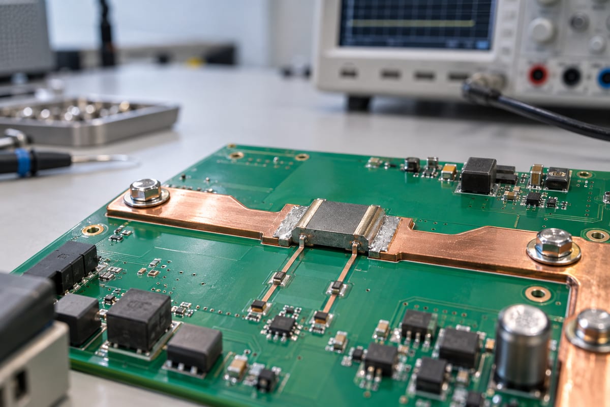
What Is Four Terminal Sensing and Why Does It Improve Low-Resistance Measurements?
Four terminal sensing, also called four-wire sensing or Kelvin sensing, separates the current-carrying connections from the voltage-measuring connections. This allows the circuit to measure the resistance element without including most of the unwanted voltage drop in the conductors and connection points.
- Force path: Two connections carry current through the resistor. Their traces, pads, and solder joints may create additional voltage drop, especially at high current.
- Sense path: Two separate connections measure voltage at the designated points on the resistor. Because the sense inputs draw very little current, voltage drop along these traces is extremely small.
This separation is especially valuable when measuring a current shunt, power connection, busbar interface, battery path, or another milliohm-level resistance. It does not eliminate errors from component tolerance, temperature coefficient, amplifier offset, noise, thermal gradients, or calibration; it specifically reduces the error introduced by shared conductors and connection resistance.
How Does Four Terminal Sensing Differ from Two-Wire Resistance Measurement?
The practical difference is whether the same conductors or separate conductors carry current and measure voltage.
- Two-wire resistance measurement: The same path carries current and measures voltage. The result can include voltage drops from PCB traces, pads, solder joints, connectors, cables, and test leads.
- Four terminal sensing: The force connections carry current, while separate sense connections measure voltage close to the resistance element. Most of the voltage drop in the high-current conductors is therefore excluded from the measurement.
For a milliohm-level shunt, even a short shared copper section can shift the reading. Moving the sense connection from the load trace to the designated point on the resistor pad can exclude that shared copper. Two-wire measurement may be sufficient when conductor resistance is insignificant, but four terminal sensing becomes more valuable as resistance decreases, current increases, or allowable error becomes tighter.
How Should a Kelvin Connection Separate Force and Sense Current Paths?
A Kelvin connection should keep the force and sense paths electrically separate until they reach the intended measurement points. If they share copper before reaching the resistor, the voltage drop across that shared section becomes part of the measurement.
- Route the force path through the load-current regions. Wider force copper should enter and leave through the parts of the pads intended to carry current and control temperature rise.
- Connect the sense traces directly to the sensing points. They should not branch from a force trace farther away from the resistor.
- Keep the two sense traces short and reasonably balanced. They should avoid switching nodes and high-current loops that may couple noise into a small differential signal.
- Place vias without creating shared load-current copper. A via may help escape a dense area, but the sense signal should not pass through copper that also carries the load current.
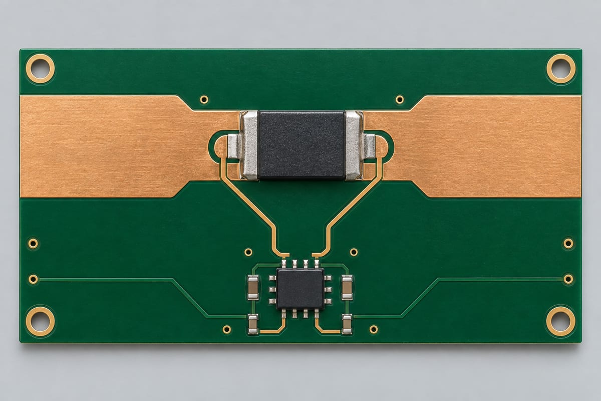
The approved PCB data should make this physical separation unambiguous so that fabrication and assembly reproduce the intended connection rather than interpret it.
Where Should Sense Traces Meet the Shunt Resistor Pads?
Sense traces should meet the shunt resistor at dedicated points that exclude unwanted voltage drop from the load-current copper and solder connections. The exact location depends on the resistor package and its approved footprint.
- For a two-terminal shunt: Each sense trace commonly approaches the inner portion of a split pad, while load current enters through a different part of the copper. This reduces the pad and trace resistance shared by the force and sense paths.
- For a four-terminal resistor: Each sense trace connects to its dedicated sense terminal. The PCB must keep that terminal separate from the force copper until the intended measurement point; reconnecting it too early can reintroduce unwanted voltage drop.
Current distribution around the pads also matters. If load current enters one side of a shunt unevenly, the voltage across the pad surface will not be uniform. Symmetrical copper entry and clearly defined sensing locations reduce the risk of a repeatable offset caused by pad resistance or solder distribution. The approved land pattern should therefore leave no uncertainty about where the measurement begins.
How Does PCB Layout Affect Four Terminal Sensing Accuracy?
PCB layout determines which voltage drops the sense circuit includes and which ones it excludes. A correct schematic can therefore produce an inaccurate assembled board if the physical current path is not controlled.
- Shared copper: Any section used by both force and sense paths can add a load-dependent voltage drop to the measurement.
- Sense-point location: Moving a sense connection along a pad or trace changes how much pad and copper resistance is included in the measured voltage.
- Current distribution: Pad shape, neck-down regions, copper pours, thermal reliefs, and nearby vias influence how current enters the resistor. Uneven entry can create unequal voltage distribution around the terminals.
- Noise coupling: Sense traces routed near switching nodes, inductors, gate-drive loops, or fast current transients can pick up noise that obscures a small differential signal.
- Thermal conditions: Heat from the shunt, power devices, or unequal copper areas can affect the resistor and nearby measurement circuitry.
The best layout is not simply the one with the shortest traces. It is the one that controls what the sense circuit measures, maintains predictable current flow, limits noise coupling, and can be reproduced consistently in fabrication and assembly.
When Should a PCB Use a Four-Terminal Resistor or a Split-Pad Footprint?
- Use a dedicated four-terminal resistor when measurement accuracy and repeatability are critical and a suitable component is available in the required resistance, power, tolerance, temperature coefficient, and package size. Its separate terminals establish a physical distinction between force and sense connections.
- Use a split-pad footprint around a two-terminal shunt when the approved BOM already specifies that component, sourcing options are limited, board space is constrained, or the customer has validated the footprint in the operating circuit.
These approaches are not automatically interchangeable. A four-terminal component reduces dependence on custom pad segmentation and makes the connection intent easier to reproduce. A split-pad footprint offers compatibility with an existing two-terminal shunt but depends more heavily on the pad geometry and current-entry pattern.
The choice should be based on electrical accuracy, power dissipation, thermal behavior, package availability, cost, board space, and validation results. After the component and footprint have been approved, their measurement-critical geometry should not be changed during DFM or production without customer review. A seemingly minor adjustment to pad divisions, copper entry, or sense-point location can change what the circuit measures.
How Can PCB Fabrication and Assembly Preserve Kelvin Sensing Accuracy?
PCB fabrication and assembly preserve Kelvin sensing accuracy by reproducing the approved force and sense geometry without introducing variations that change current flow or connection resistance.
- During fabrication: The split-pad spacing, copper entry, sense-trace connection points, vias, and solder-mask boundaries must remain consistent with the approved data. Unauthorized copper smoothing or pad modification near the shunt can alter the electrical boundary even when the board remains fully connected.
- During assembly: Solder-paste distribution and component placement are especially important around divided or asymmetric pads. Excessive placement offset or uneven solder volume can change how the terminals contact the pads and how current enters the resistor. The assembly process should also avoid solder bridging across regions intended to remain electrically distinct.
- AOI: Confirms component position, orientation where applicable, and visible solder conditions.
- X-ray: Helps examine relevant joints or structures that are hidden from optical inspection.
- Electrical testing: Verifies measurement performance when the customer defines the limits, current conditions, fixtures, and procedures for the intended application.
AOI and X-ray can verify assembly quality, but they do not by themselves prove sensing accuracy. Electrical testing is required when the finished PCBA must be evaluated against a defined measurement limit.

When critical pad geometry, solder volume, and component placement remain consistent, a validated prototype is more likely to move into repeat production without unexpected measurement shifts between batches.
FAQs About Four Terminal Sensing
Is four terminal sensing the same as Kelvin sensing? In most PCB current-measurement applications, yes. Both terms describe the use of separate force and sense connections so that conductor and contact resistance in the force path has less influence on the measured voltage.
Does four terminal sensing require a four-terminal resistor? No. A dedicated four-terminal resistor provides separate physical terminals, but a validated split-pad footprint can create Kelvin connections around a two-terminal shunt. The component and footprint must be evaluated together.
Can four terminal sensing eliminate all current-measurement errors? No. It primarily reduces errors caused by shared conductor and connection resistance. Resistor tolerance, temperature coefficient, amplifier errors, noise, thermal effects, and calibration can still affect the complete measurement.
Why can boards made from the same schematic produce different readings? The schematic does not define every physical detail of current flow. Differences in sensing-point location, pad geometry, copper distribution, solder volume, component placement, and temperature can change the measured voltage even when the electrical connections appear identical.
Should Kelvin sense traces be routed as a differential pair? They should generally be kept close, balanced, and away from noise sources, but the required geometry depends on bandwidth, amplifier architecture, signal level, and the customer’s circuit. They should not automatically be treated as a controlled-impedance high-speed differential pair.
Can a PCB manufacturer change the Kelvin footprint during DFM? A manufacturer may identify a manufacturability concern and recommend a change, but it should not silently alter measurement-critical geometry. Changes to sense-point locations, split pads, copper entry, or terminal assignments require customer review and approval.
EBest Circuit manufactures and assembles customer-designed PCBs and PCBAs with Kelvin connections, from prototypes through repeat production. We focus on preserving the approved force and sense separation through PCB fabrication, component placement, soldering, inspection, and agreed testing so the finished board can deliver more consistent low-resistance measurements. If you are preparing a four terminal sensing PCB or PCBA, send your Gerber files, BOM, assembly data, quantities, and testing requirements to sales@bestpcbs.com for a manufacturability review and quotation.
You may also like


Tags: Four Terminal Sensing, Four-Wire Resistance Measurement, Kelvin connection