PCB manufacturing PCB manufacturing
Home > Blog

UHDI printed circuit board

UHDI Printed Circuit Board: Design Rules, Stackup, and DFM
Tuesday, September 1st, 2026

A UHDI printed circuit board moves beyond conventional HDI when at least one critical feature enters the ultra-fine range. That change affects far more than trace width. The imaging method, copper build, microvia geometry, dielectric thickness, registration plan, solder mask, inspection criteria, and assembly interface must be treated as one manufacturing system.

This guide helps design and procurement teams decide whether a project is truly UHDI, where early DFM work prevents redesign, and what evidence should be agreed before prototype release. It also separates published working thresholds from a supplier’s confirmed production capability—an important distinction when yield, reliability, and repeatability matter.
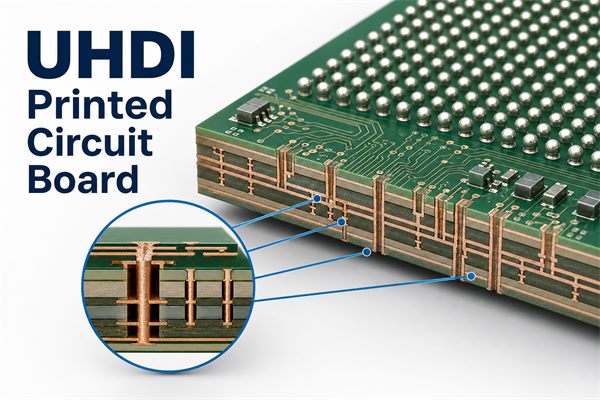
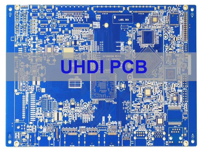
UHDI printed circuit board with ultra-fine traces and laser microvias

What Is a UHDI Printed Circuit Board?

UHDI means ultra-high-density interconnect. The industry’s working definition generally places a board in UHDI territory when one or more features go beyond the highest conventional HDI producibility range. Common reference thresholds include:

  • Conductor line width below 50 µm.
  • Conductor spacing below 50 µm.
  • Build-up dielectric thickness below 50 µm.
  • Laser microvia diameter below 75 µm.

These figures are useful screening points, not permission to combine every minimum on one design. A board with 45 µm spacing on one layer may require a different process route from a board with 60 µm traces and 50 µm microvias. Material, copper thickness, panel format, feature distribution, registration tolerance, surface finish, and annual volume all affect the real production window.

The shorter phrase ultra hdi pcb often refers to the same technology. In practice, the fabrication drawing should state the actual features and acceptance requirements instead of relying on the label alone.

How Does UHDI Differ from Conventional HDI?

Conventional HDI gains density through laser microvias, blind or buried connections, sequential lamination, and via-in-pad. UHDI keeps those concepts but pushes selected geometries beyond conventional HDI process limits. That shift changes both the fabrication method and the amount of process verification required.

Design Area Conventional HDI UHDI Consideration
Fine conductors Often produced by optimized subtractive etching May require mSAP, SAP, or another ultra-fine-line process
Microvias Laser-drilled vias commonly around the 0.10 mm class Smaller geometry needs tighter drilling, plating, and registration control
Dielectrics Build-up films selected around a proven HDI stackup Very thin dielectrics make copper balance and via aspect ratio more sensitive
Inspection AOI, electrical test, impedance test, and microsection as specified More detailed coupons, dimensional evidence, and agreed acceptance rules may be needed

A designer should therefore ask, “Which features require UHDI?” rather than applying ultra-fine geometry across every layer. Restricting the most demanding rules to the package escape or other density-critical zones can improve yield and cost without sacrificing electrical performance.

HDI PCB Design Guidelines for UHDI Layouts

Useful hdi pcb design guidelines begin with the fabricator’s production window, not the CAD tool’s minimum setting. The following decisions should be closed before routing is frozen:

  • Define the density driver. Record BGA pitch, pad diameter, escape count, available routing channels, and the layers that genuinely need ultra-fine features.
  • Use regional rules. Keep wider traces and spaces outside dense package fields where possible. A mixed-rule design is usually easier to control than a board built entirely at the minimum.
  • Separate line and space values. Do not assume a supplier’s minimum line width automatically permits the same minimum clearance after plating.
  • Coordinate copper with geometry. Thicker copper is harder to resolve into very fine conductors. Base copper and final copper must both appear in the fabrication notes.
  • Treat solder mask as a precision layer. Mask registration, dam width, pad definition, and via treatment can determine whether fine-pitch assembly is practical.
  • Control impedance from the real stackup. Trace geometry, dielectric thickness, resin content, copper profile, and reference-plane distance must be reviewed together.

Do not design every feature at a supplier’s stated limit. The published minimum may describe a test coupon or a restricted build, while the stable production value may be wider. A useful DFM conversation distinguishes prototype feasibility, repeatable production, and the conditions attached to each.
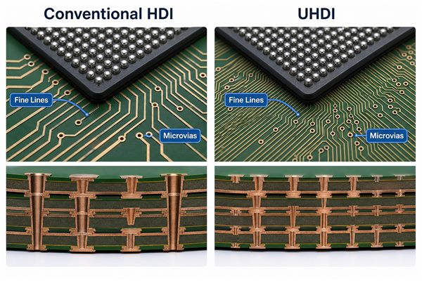
Comparison of conventional HDI and UHDI PCB trace and microvia geometry

HDI PCB Stackup Decisions for UHDI

An hdi pcb stackup cannot be finalized independently from the escape strategy. The number of build-up layers, microvia spans, plane assignment, material family, and impedance targets determine the lamination sequence and the inspection plan.

Review these points together:

  • Build-up architecture: confirm whether 1+N+1, 2+N+2, any-layer, or another construction is actually required.
  • Microvia type: use staggered microvias where routing permits; specify stacked structures only where density justifies the additional process and reliability burden.
  • Via aspect ratio: match microvia diameter to dielectric depth. A small opening through an unnecessarily deep dielectric creates plating risk.
  • Via fill and cap: via-in-pad normally requires a defined fill, planarization, and cap-plating sequence before component assembly.
  • Stack symmetry: balance copper and dielectric construction to reduce bow, twist, and registration drift through repeated thermal cycles.
  • Material availability: confirm the exact laminate, build-up film, copper foil profile, thickness tolerance, and approved substitutes before impedance values are released.

Early stackup review is especially important when UHDI routing is combined with high-speed interfaces. Our existing guide to HDI PCB structures explains conventional 1+N+1, 2+N+2, and every-layer interconnect concepts, while the separate 80 GHz UHDI PCB article focuses on RF material and impedance concerns.
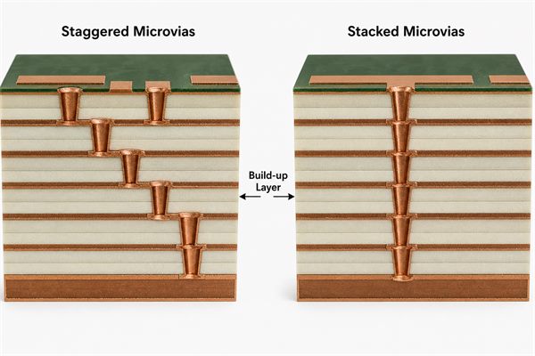
UHDI PCB stackup showing staggered and stacked laser microvias

How Does the HDI PCB Manufacturing Process Change for UHDI?

The hdi pcb manufacturing process normally uses sequential build-up, laser drilling, copper deposition, imaging, plating, lamination, and electrical verification. UHDI adds tighter interactions between these steps and may change the conductor-forming method.

  1. Engineering review: identify every sub-50 µm feature, microvia span, impedance structure, copper requirement, and inspection coupon.
  2. Material and process selection: choose a laminate, build-up dielectric, copper foil, and imaging route that can hold the requested geometry.
  3. Core and build-up imaging: form fine conductors with a process selected for the target line, space, and copper thickness.
  4. Laser drilling and desmear: control via diameter, taper, landing accuracy, and the condition of the target pad.
  5. Metallization and filling: establish reliable copper in the microvia, fill specified structures, and planarize via-in-pad surfaces.
  6. Sequential lamination: repeat build-up cycles while controlling registration, resin flow, copper balance, and thickness.
  7. Surface formation: apply solder mask and surface finish without consuming the clearances needed for fine-pitch assembly.
  8. Inspection and test: use AOI, electrical testing, microsection, dimensional measurement, impedance testing, or other project-specific evidence.

Subtractive etching can support some near-UHDI geometries, but very fine and consistent conductors may require modified semi-additive or semi-additive processing. The correct route depends on feature size, copper thickness, layer location, panel scale, volume, and supplier capability. It should be confirmed before the layout is locked.

Which DFM Risks Cause UHDI Prototype Failure?

UHDI prototypes most often become expensive when a local density decision triggers an unplanned process change. The risk is rarely one number in isolation.

  • Minimum geometry used everywhere: reduces the process margin across the whole panel even though only a small BGA area needs it.
  • Excessive stacked microvias: increases lamination count and concentrates thermo-mechanical stress.
  • Unconfirmed copper build: fine lines may not survive the plating and etching sequence at the requested final copper.
  • Ambiguous via notes: missing fill, cap, target-layer, or aspect-ratio requirements can change both cost and reliability.
  • Late impedance modeling: forces trace-width or dielectric changes after routing is complete.
  • Insufficient mask clearance: causes assembly constraints even when the copper pattern can be fabricated.
  • No agreed acceptance plan: leaves the customer and supplier evaluating fine features with different criteria.

A strong DFM response should show what must change, why it matters, and whether the recommendation affects electrical performance. “Cannot build” is not enough; the customer needs an alternative feature, stackup, or process route.

What Inspection Evidence Should Be Defined?

Electrical continuity alone cannot prove that a UHDI process is stable. The inspection plan should follow the critical risks in the design and may include:

  • AOI coverage for fine-line layers.
  • Microsection locations that represent stacked or staggered microvias.
  • Measurement of finished line width, spacing, dielectric thickness, and via geometry.
  • Impedance coupons that match the controlled layers and copper construction.
  • Electrical test coverage and netlist source.
  • Surface-finish thickness or wire-bond acceptance criteria when applicable.
  • Assembly X-ray or other inspection for fine-pitch packages when the project includes PCBA.

At EBest Circuit, our documented quality resources include AOI, electrical testing, impedance testing, microsection inspection, copper-thickness testing, 2D measurement, and X-ray inspection for relevant assembly work. The final test plan still depends on the product, customer specification, and confirmed process route. See our PCB quality and testing overview for the broader control framework.
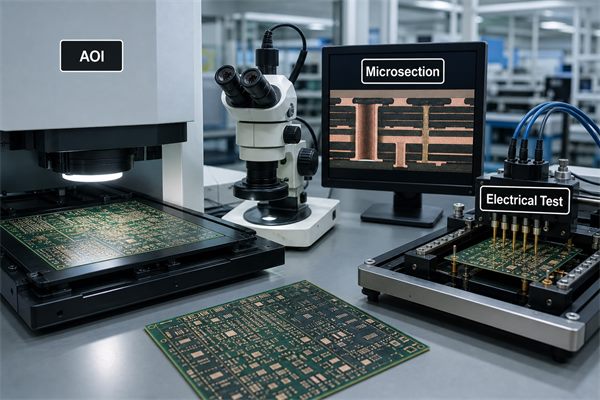
UHDI PCB microsection and automated optical inspection workflow

How Do UHDI Choices Affect Cost and Lead Time?

UHDI does not automatically make the lowest system cost, even when it reduces board area. Cost and lead time rise when a design adds specialized material, semi-additive conductor formation, more lamination cycles, stacked microvias, tight registration, extra coupons, or low-yield feature combinations.

The practical cost levers are:

  • How many layers actually need ultra-fine line and space.
  • Whether a standard panel and material construction can be used.
  • The number of sequential lamination cycles.
  • Staggered versus stacked microvia architecture.
  • Base and finished copper thickness.
  • Surface finish and fine-pitch assembly requirements.
  • Prototype quantity, test evidence, and volume forecast.

A compact UHDI board can still lower total product cost when it removes connectors, reduces board area or layer count, shortens critical interconnects, or enables a smaller enclosure. The comparison should therefore use total system impact, not PCB unit price alone.

What Should Be Included in a UHDI RFQ Package?

Provide enough information for the supplier to evaluate the exact feature combination. A useful package includes:

  • Gerber or ODB++ fabrication data and the fabrication drawing.
  • Proposed layer stackup, material family, finished thickness, and copper weights.
  • A list of the minimum line, minimum spacing, smallest microvia, and affected layers.
  • Microvia spans, stacked or staggered structure, via fill, and cap-plating notes.
  • Controlled-impedance table and reference-layer information.
  • Surface finish, solder mask, legend, and assembly constraints.
  • Test standard, inspection evidence, coupon requirements, and acceptance class.
  • Prototype quantity, expected annual volume, and requested delivery date.
  • BOM, pick-and-place data, and assembly drawing when PCBA is required.

For a general supplier overview, you can also review our existing UHDI PCB fabrication page. Its purpose is supplier selection, while this page is intended to help engineering teams prepare a manufacturable design package.

FAQ About UHDI Printed Circuit Boards

Is every board with microvias a UHDI PCB?

No. Microvias are common in conventional HDI. UHDI is associated with one or more features beyond conventional HDI thresholds, such as sub-50 µm lines or spaces, sub-50 µm build-up dielectrics, or microvias below the 75 µm range.

Does UHDI always require mSAP?

No. The conductor-forming method depends on the target geometry, copper thickness, layer, panel, and supplier. Some near-UHDI features may be possible with advanced subtractive control, while tighter and more uniform conductors may need mSAP or SAP.

Are stacked microvias better than staggered microvias?

Not automatically. Stacked microvias save routing area, but they add process complexity and reliability sensitivity. Use them where density requires them; use staggered structures where the layout allows a more forgiving construction.

Can standard HDI design rules be reused for UHDI?

They are a starting point, not a release condition. UHDI requires a supplier-specific review of fine-line formation, dielectric depth, via geometry, copper build, registration, solder mask, inspection, and production volume.

How Can EBest Circuit Review Your UHDI Project?

EBest Circuit has provided PCB and PCBA support since 2006. We work with customers on PCB design review, prototyping, multilayer and HDI fabrication, component sourcing, assembly, and testing. Our documented management and compliance resources include ISO 9001:2015, ISO 13485:2016, IATF 16949, AS9100D, UL, RoHS, and REACH; applicability should be confirmed for the specific product and production route.

For a true UHDI request, we do not treat a marketing label as a capability approval. Our team first reviews the line and space by layer, dielectric construction, microvia geometry, copper build, stackup, impedance, surface finish, quantity, and required evidence. We then confirm whether the project fits an available process route or needs design adjustment. You can also review our broader PCB manufacturing capability information.

Send your Gerber or ODB++ files, stackup, impedance table, fabrication drawing, quantity, and test requirements to sales@bestpcbs.com. We will help identify the density-critical features, return practical DFM feedback, and confirm a manufacturable path for your UHDI printed circuit board before quotation.


You may also like

Custom UHDI PCB Manufacturer | Quick Prototype Fabrication
Thursday, April 2nd, 2026

UHDI PCB​ represents the pinnacle of high-density interconnect technology, enabling the advanced miniaturization and superior performance required by next-generation electronics. This comprehensive guide delves into everything you need to know about UHDI PCBs, from their fundamental definition and materials to design considerations and how to select the right manufacturing partner for your prototype and production needs.

What are the core pain points when sourcing UHDI PCBs?

  • Finding True Expertise:​ Many manufacturers claim HDI capability, but few possess the specialized equipment and process control for genuine UHDI features like 25µm line/space and microvias below 50µm.
  • Prototype Delays:​ Critical R&D and testing phases are stalled by long lead times for complex UHDI prototypes, delaying time-to-market for cutting-edge products.
  • Unpredictable Costs:​ Opaque pricing structures and unexpected engineering charges for impedance control and advanced materials like Megtron 6 or Rogers make budgeting difficult.
  • Design for Manufacturing (DFM) Gaps:​ A lack of proactive engineering support leads to design revisions, respins, and failures because the board wasn’t optimized for UHDI fabrication processes.
  • Fragmented Supply Chain:​ Managing separate vendors for design, PCB fabrication, assembly, and testing adds complexity, risk, and communication overhead.

Best Technology provides integrated solutions to these exact challenges.​ As a specialized UHDI PCB manufacturer, we bridge the gap between ambitious design and reliable, high-yield manufacturing.

  • Proven UHDI Process Mastery:​ Our investment in technology like laser direct imaging and advanced laser drilling allows us to reliably produce 2/2 mil lines and 0.1mm microvias, meeting the stringent demands of UHDI circuits.
  • Rapid Prototype Service:​ We prioritize quick-turn UHDI PCB prototype fabrication, with expedited services available to get your boards in hand for testing in as little as 48-72 hours for multilayer builds, accelerating your development cycle.
  • Transparent and Competitive Pricing:​ We offer clear, upfront quotations for prototype and volume production, with cost breakdowns for different quantities (e.g., 1 pc, 100 pcs, 1000 pcs) and materials, ensuring no surprises.
  • Expert DFM and Stack-up Support:​ Our engineering team works with you from the start, providing preliminary stack-up structures and impedance modeling guidance (e.g., for 80 GHz applications) to ensure your design is manufacturable and performs as intended.
  • Full Turnkey Service:​ From UHDI printed circuit board fabrication and component sourcing to precise assembly and rigorous testing, we offer a one-stop solution, simplifying your supply chain and ensuring accountability.

EBest Circuit (Best Technology) is a premier and experienced UHDI PCB manufacturer in China. With 20 years of dedicated PCB fabrication expertise, we have evolved into a trusted full-turnkey solution provider. We specialize in advanced technologies including UHDI, RF/microwave PCBs (using Rogers, Taconic, Megtron materials), heavy copper, and rigid-flex boards. Our commitment is underscored by ISO9001, IATF16949, and ISO13485 certifications, and a 97% on-time delivery rate. We combine state-of-the-art equipment with deep engineering knowledge to deliver high-quality, high-precision PCBs for the most demanding applications. For your UHDI project, pls feel free to contact our experts at sales@bestpcbs.com.

What Is a UHDI PCB?

A UHDI (Ultra High-Density Interconnect) PCB is an advanced type of printed circuit board characterized by exceptionally fine features, which enable a dramatically higher wiring density within a given area compared to standard HDI or traditional PCBs. This is achieved through extremely narrow trace widths/spacing, smaller microvias, and higher interconnect pad density.

Key characteristics defining a UHDI circuit board include:

  • Extremely Fine Lines/Spaces:​ Feature sizes of 30µm (1.2 mil) and below, pushing towards 25µm (1 mil) or less. Our capabilities support advanced HDI features down to 2/2 mil.
  • Microvias:​ Extensive use of laser-drilled microvias with diameters below 75µm (3 mil), often in stacked or staggered configurations. Our equipment allows for minimum laser-drilled via diameters of 4 mil (0.1mm).
  • High Layer Count:​ Often involves 10+ layers to accommodate complex routing in compact spaces. We can manufacture up to 32-layer multilayer boards.
  • Advanced Materials:​ Frequent use of high-performance, low-loss laminate materials to ensure signal integrity at high speeds.
  • Any-Layer Interconnection:​ The most advanced form where microvias can connect any two layers in the stack-up, maximizing routing freedom.

In essence, a UHDI printed circuit board (PCB) is the enabling hardware for today’s most compact and high-performance electronic devices, such as advanced smartphones, wearable technology, and high-speed computing modules, where real estate is at a premium and signal speeds are critical.

What Is the Difference Between a UHDI PCB and an HDI PCB?

While both HDI (High-Density Interconnect) and UHDI PCBs aim to increase wiring density, UHDI represents a significant evolution and a higher tier of capability. Think of HDI as the foundation and UHDI as the specialized, cutting-edge extension of that technology.

The primary differences are quantitative and qualitative advances in manufacturing tolerances and design rules:

FeatureHDI PCBUHDI PCB
Line/Space (Typical)3/3 mil (75/75 µm) and above2/2 mil (50/50 µm) and below, targeting ≤1/1 mil
Microvia Diameter≥4 mil (100 µm)≤3 mil (75 µm), targeting 1-2 mil
Pad SizeRelatively largerExtremely small, often at the limit of registration accuracy
Interconnect DensityHighUltra-High
Primary DriverSpace saving, moderate performanceMaximum miniaturization, highest signal integrity for high-speed/frequency
Manufacturing ProcessAdvanced laser drilling, sequential laminationSame as HDI, but with tighter process control, more advanced imaging (e.g., LDI), and often more lamination cycles.

In summary, all UHDI PCBs are HDI, but not all HDI PCBs qualify as UHDI. UHDI pushes the boundaries of HDI technology to its extremes, requiring more precise and controlled manufacturing processes. For instance, our standard HDI capability offers 3/3 mil lines, while our advanced processes support the 2/2 mil features that edge into UHDI territory, demonstrating the technical progression.

What Is the Difference Between a UHDI PCB and an RF PCB?

This is a crucial distinction: UHDI and RF PCB are classifications based on different primary objectives. One focuses on density, the other on signal performance​ at high frequencies. They are not mutually exclusive and often converge in advanced applications.

AspectUHDI PCBRF PCB
Primary GoalMaximize density & miniaturization.Signal integrity at high frequency.
Key MetricFine features (line/space, via density).Material properties (Dk/Df).
Critical MaterialsAdvanced FR4, thin cores.Specialized low-loss laminates (e.g., Rogers, Megtron).
Design FocusRouting complexity & microvias.Transmission line geometry & grounding.
Typical ApplicationsMobile, wearable, compact devices.5G/6G, radar, satellite comms.

The convergence of these two technologies results in what is known as an RF UHDI PCB. The most advanced boards, like the one mentioned in the customer inquiry for 80 GHz operation, must be both. They require the ultra-fine features of UHDI to route high-density, high-pin-count RF components and​ the specialized materials (like Megtron 6 or Rogers) of an RF PCB to maintain signal integrity at such extreme frequencies. Manufacturing such a board requires a vendor proficient in both domains—handling advanced materials with precise impedance control while executing UHDI-level fine features and microvia structures.

What Material Is a UHDI PCB Made Of?

The materials for a UHDI PCB are selected to support both the fine-feature fabrication processes and the intended electrical performance, often high-speed or high-frequency.

Core Material Systems:

  1. Standard & High-Performance FR4:For UHDI applications not at the extreme high-frequency edge, high-Tg FR4 (Tg ≥ 170°C) like KB6167 or IT180 is common. It offers good stability for sequential lamination cycles. Our material inventory includes high-Tg, no-halogen FR4 options suitable for complex multilayers.
  2. Low-Loss / High-Speed Laminates:For UHDI boards where signal integrity is paramount, materials with a lower dissipation factor (Df) are mandatory. This includes:
    • Megtron 6/7/8 (Panasonic):​ A popular choice for high-speed digital and RF applications, offering excellent electrical properties.
    • Rogers RO4000® Series:​ Ceramic-filled hydrocarbon laminates ideal for RF and microwave designs.
    • Isola FR408HR, Nelco N4000-13:​ Other high-performance options for demanding electrical environments.
  3. Thin Dielectric Laminates and Prepregs: UHDI relies on very thin core and prepreg layers (e.g., 1080, 106, 1035 styles) to achieve the close layer spacing needed for microvias and controlled impedance in dense layouts. We utilize a wide range of PP types, including 1080 (0.07mm), 2116 (0.11mm), and 7628 (0.175mm).
  4. Advanced Copper Foils:Treated or very low-profile copper foils are used to improve adhesion and etching yields for extremely fine traces.

The choice of material is dictated by the application’s frequency, data rate, thermal, and reliability requirements.​ For the 80 GHz application specified in the inquiry, Megtron 6 or Rogers​ would be the recommended substrate materials to meet the low-loss demands at that frequency, fabricated using UHDI processes.

How to Design the Preliminary Stack-Up Structure of a UHDI Printed Circuit Board?

Designing the stack-up is a foundational step in UHDI PCB development, critical for impedance control, signal integrity, power integrity, and manufacturability. A well-planned stack-up saves multiple prototyping cycles.

A step-by-step approach for a preliminary UHDI PCB stack-up design:

  • Define Requirements:​ Start with the board’s functional needs: number of signal layers, power/ground planes, target impedance (e.g., 50Ω single-ended, 100Ω differential), operating frequency (e.g., 80 GHz), and board thickness constraints.
  • Select Core Material:​ Based on frequency/speed, choose the dielectric material (e.g., Megtron 6 for RF, High-Tg FR4 for high-density digital). Obtain its certified Dk and Df values at your target frequency from the manufacturer’s datasheet.
  • Determine Dielectric Thickness:​ This is the distance between adjacent copper layers. For UHDI, these are often very thin (e.g., 2-4 mils) to enable microvias and tight coupling. Use an impedance calculator (like Polar Si9000) with the material Dk, target impedance, and desired trace width to solve for the required dielectric thickness.
  • Choose Copper Weight:​ Thinner copper (e.g., ½ oz or 1/3 oz) is preferred for etching fine traces. Standard UHDI designs often use ½ oz (17.5 µm) finished copper for signal layers. Heavier copper (1 oz+) may be used for power planes.
  • Arrange Layer Sequence:​ Follow a symmetrical stack-up to prevent warpage. Use a signal-ground-signal (S-G-S) sandwich for critical high-speed lines to provide a clear return path. Place power and ground planes adjacent to each other to form a decoupling capacitor.
  • Plan the Via Strategy:​ Decide on via types: through-hole vias, blind vias (from surface to inner layer), buried vias (between inner layers), and microvias (typically <6 mil diameter). In UHDI, microvias are key. Plan their depth (1-n layers) and whether they will be stacked or staggered.
  • Consult Your Manufacturer Early:​ Engage with your UHDI PCB manufacturer (like Best Technology) during this phase. Share your target stack-up for a DFM review. We can provide feedback on material availability, feasible dielectric thicknesses, and recommend adjustments for optimal yield and performance.

Example Preliminary Stack-Up for a 12-Layer UHDI/RF Board:

LayerTypeMaterial/ThicknessDescription
L1Signal½ oz CuTop Layer, RF Components
Dielectric3.5 mil Megtron 6
L2Ground1 oz CuSolid Ground Plane
Dielectric4 mil Prepreg
L3Signal½ oz CuHigh-Speed Signals
Core4 mil Megt6 Core
L4Power1 oz CuPower Plane 1
L12Signal½ oz CuBottom Layer

This is a simplified example. The actual design would be built in collaboration with our engineers.

Where Is a UHDI PCB Used?

UHDI PCBs are indispensable in industries where miniaturization, high performance, and reliability are non-negotiable. Their ability to pack immense functionality into a tiny footprint makes them the backbone of modern advanced electronics.

Primary application areas for UHDI printed circuit boards include:

  • Consumer Electronics:​ Smartphones, tablets, laptops, and wearables (smartwatches, AR/VR headsets) constantly push for smaller, lighter, and more powerful devices.
  • Medical Electronics:​ Implantable devices (pacemakers, neurostimulators), advanced diagnostic imaging equipment, and miniature surgical tools.
  • Telecommunications & 5G/6G Infrastructure:​ RF front-end modules, millimeter-wave antennas, base station processing units, and network switches operating at extremely high frequencies.
  • Automotive Electronics:​ Advanced Driver-Assistance Systems (ADAS), LiDAR sensors, infotainment systems, and vehicle control units in electric and autonomous vehicles.
  • Aerospace and Defense:​ Avionics, satellite communication systems, radar, and guidance systems where reliability and performance in harsh environments are critical.
  • High-Performance Computing (HPC):​ Servers, data centers, and AI accelerator modules that require high-speed data transfer between densely packed components.

In each case, the UHDI circuit board enables a critical size reduction or performance enhancement that would be impossible with conventional PCB technology.

Top 10 UHDI Circuit Board Manufacturers in China

Identifying the “top” manufacturers depends heavily on specific project needs—prototype vs. volume, technology focus (e.g., RF UHDI), and industry vertical. Rather than a simple list, here are key criteria for evaluation and how Best Technology positions itself:

Key Evaluation Criteria for a UHDI PCB Manufacturer:

  • Technology Certification:​ Demonstrated capability in ≤ 3/3 mil line/space, microvia drilling ≤ 4 mil, and any-layer HDI processes. We support 2/2 mil lines and 4 mil (0.1mm) laser-drilled microvias.
  • Material Expertise:​ Proven experience with high-frequency laminates (Rogers, Taconic, Megtron) and high-Tg materials. Our material portfolio includes these advanced substrates.
  • Advanced Equipment:​ Investment in LDI (Laser Direct Imaging) for fine-line patterning, high-precision laser drills, and AOI (Automatic Optical Inspection). We utilize equipment from global leaders like Hitachi (drilling) and Israeli AOI systems.
  • Engineering Support:​ Strong DFM and stack-up design support team. Our engineers provide preliminary stack-up structures for impedance matching.
  • Quality Systems:​ Certifications like IATF 16949 (automotive) and ISO 13485 (medical) indicate process rigor. We hold these certifications, among others.
  • Prototype Speed:​ Willingness and ability to offer quick-turn prototype services. We provide expedited 24-72 hour turns for multilayer prototypes.
  • Volume Scalability:​ Capacity to scale from prototype to medium/high-volume production seamlessly. Our monthly capacity is over 28,900 square meters.
  • Testing Capability:​ In-house electrical testing, impedance testing, and reliability testing. We employ flying probe testers, universal E-testers, and micro-section analysis.
  • Vertical Integration:​ Offering turnkey services (PCB + Assembly) reduces supply chain risk. We are a full turnkey provider.
  • Customer Service & Communication:​ Responsive, technical sales and project management. We pride ourselves on one-on-one engineering support and fast response times.

Top 10 UHDI Circuit Board Manufacturers in China (Reference Table)

CompanyProcess CapabilityPrototype Lead Time
EBest Circuit (Best Technology)1+N+1 to 3+N+3; PTH ≤0.1mm24 hours
PCBWayMicrovias; 0.10mm laser hole; 55/55μm L/S24 hours
PCBCartHDI; 2.5 mil trace/space2 days to 5 weeks
JLCPCBBlind/buried vias; 0.15mm via hole24–72 hours
OurPCB2.5 mil trace/space; 0.1mm microvia24 hours to 7 days
RayPCB3 mil trace/space; ~150μm via1–5 days
KKPCB2/2 mil L/S; 0.075–0.15mm laser drillTo be confirmed
WellPCB1.8 mil spacing; microvia supportAbout 2 weeks
Weller PCB2/2 mil HDI; microvias <150μm1–2 days
PCBBUY2/2 mil HDI; ≥0.075mm blind via24 hours to 7 days

Note: The ranking above is for reference only. The right UHDI PCB manufacturer should be selected based on your required line/space, microvia structure, material system, stack-up complexity, prototype speed, and volume production needs.

Why Choose EBest Circuit (Best Technology) for UHDI PCB Prototype Fabrication?

Selecting the right partner for your UHDI prototype is critical to project success. Best Technology is engineered to be that partner, offering a unique blend of advanced capability and responsive service.

  • Proven Advanced Technology Foundation:​ Our core manufacturing capabilities are tailored for complexity. We routinely handle ultra-fine features (3/3 mil standard, 2/2 mil advanced HDI), high layer counts (up to 32 layers), and controlled impedance (tolerance ±10% for >50Ω, ±5Ω for ≤50Ω). Our expertise in heavy copper (up to 20 oz) and various substrates (FR4, MCPCB, Ceramic) translates to robust process control for delicate UHDI structures.
  • Dedicated Quick-Turn Prototype Service:​ We understand the urgency of innovation. For standard-specification FR4 prototypes under 1 sq meter, we offer rapid turnaround (e.g., 10 days for 6-layer, 72 hours for expedited service). This service extends to complex builds, allowing you to iterate and validate designs quickly, compressing your R&D timeline.
  • Comprehensive Quality and Reliability Assurance:​ Quality is integrated into our process. We hold ISO 9001:2015, IATF 16949:2016, and ISO 13485:2016 certifications. Our inspection regime includes Automated Optical Inspection (AOI) from industry leaders, X-ray copper thickness testers, flying probe testing, and micro-section analysis to validate every microvia and trace.
  • Expert Engineering Partnership:​ We don’t just manufacture; we collaborate. Our engineering team provides proactive DFM feedback, assists with material selection (crucial for 80 GHz RF UHDI boards), and delivers preliminary stack-up structures for your impedance modeling. We help bridge the gap between your design and a manufacturable, high-performance product.
  • Full Turnkey Solution and Support:​ From the initial UHDI PCB prototype quote to final box build, we provide a seamless, accountable journey. Our one-stop service covers PCB fabrication, component sourcing, PCB assembly (with capabilities for 01005 components and 0.25mm BGA pitch), and testing. You get a single point of contact, simplified logistics, and faster overall project completion.

How to Request a Quote for UHDI PCB Prototype Fabrication?

Requesting a quote for a UHDI PCB is straightforward when you provide the right information. A complete and clear request ensures an accurate, fast, and competitive quotation. Here is a step-by-step guide based on common requirements, like those from the Technion inquiry:

  1. Prepare Your Design Files:​ The essential package includes your Gerber files (RS-274X format preferred), drill files, and a completed PCB fabrication drawing​ with all critical dimensions, tolerances, and notes.
  2. Specify Technical Requirements:Create a separate document detailing:
    • Layer Count & Stack-up:​ Preferred materials (e.g., “Megtron 6 for all layers” or “Rogers 4350B for L1-L4”).
    • Finished Board Thickness & Tolerance.
    • Copper Weight:​ For inner and outer layers (e.g., ½ oz inner, 1 oz outer).
    • Surface Finish:​ Specify one, e.g., ENIG, ENEPIG, Immersion Silver, Hard Gold (for edge connectors).
    • Impedance Control:​ Target values, tolerance (e.g., 50Ω ±10%), and which layers/differentials are controlled.
    • Special Requirements:​ Any specific needs like filled/via-in-pad, edge plating, or tight impedance tolerances for RF sections.
  3. Define Quantity and Urgency:
    • Clearly state the quantities you need quotes for: Prototype quantity (e.g., 5 pcs), 100 units, and 1000 units.​ This allows us to show volume pricing breaks.
    • Indicate your required lead time​ (e.g., “Standard” or “Expedited”).
  4. Request a Preliminary Stack-Up (if needed): If you are in the early design phase (like the 80 GHz application mentioned), you can request that we provide a preliminary stack-up structure​ based on your material choice and impedance targets. This allows you to perform accurate impedance modeling in your design tools.
  5. Submit and Engage: Send your complete package to sales@bestpcbs.com. A dedicated engineering sales person will review your files, may ask clarifying questions, and will provide a formal quotation typically within 24 hours, including unit price, volume pricing, and lead time options.

In closing, UHDI PCBs​ are the critical hardware foundation enabling the relentless march of electronic miniaturization and performance enhancement across industries from healthcare to telecommunications. This article has explored the what, why, and how of UHDI technology, the key differences from HDI and RF PCBs, and the practical steps involved in designing and procuring these advanced boards.

EBest Circuit (Best Technology)​ stands as a reliable specialist in this field. With two decades of experience, certified quality systems, advanced manufacturing capabilities supporting fine features and advanced materials, and a commitment to fast-turn prototypes and full turnkey solutions, we are equipped to bring your most challenging UHDI circuit board designs to life. Pls feel free to contact our technical sales team anytime at sales@bestpcbs.com​ for a comprehensive consultation and quotation.

FAQs About UHDI PCBs

1. What is the minimum line/space Best Technology can achieve for UHDI prototypes?

We regularly manufacture advanced HDI boards with 3/3 mil (75/75 µm) line/space. For designs pushing into UHDI territory, we have the capability to support 2/2 mil (50/50 µm) features, subject to a full DFM review of your specific design.

2. Can you handle the RF materials like Rogers or Megtron 6 required for high-frequency UHDI boards?

Yes, absolutely. We have extensive experience processing high-frequency, low-loss laminates including the Rogers series (e.g., RO4003C, RO4350B), Taconic, and Panasonic’s Megtron 6/7. We can guide you on material selection for applications like 80 GHz and ensure proper lamination and impedance control.

3. What is the typical lead time for a 10-layer UHDI PCB prototype?

For a standard 10-layer FR4 prototype (<1 sq. meter), our typical lead time is 12 business days. We offer expedited services that can significantly reduce this time. The lead time for a UHDI board with advanced materials (like Megtron 6) and features will be confirmed upon review of your specific technical files.

4. Do you provide impedance control and testing reports?

Yes. We have in-house impedance modeling expertise and can control impedance to tight tolerances (e.g., ±10% for values >50Ω, ±5Ω for ≤50Ω). We can provide impedance test coupons on the panel and, upon request, supply test reports to verify performance.

5. Do you offer turnkey services including component sourcing and assembly for UHDI PCBA?

Yes, we are a full turnkey provider. We can manage the entire process: manufacturing the UHDI printed circuit board, sourcing all components from authorized distributors, performing precise SMT assembly (handling 01005 components and 0.25mm BGA pitch), and conducting full functional testing. This simplifies your supply chain and ensures accountability.

You may also like