A 14 layer HDI PCB combines 14 copper layers with high-density interconnect features such as microvias, blind and buried vias, sequential lamination, and via-in-pad.
The extra layers provide room for signals, ground planes, and power distribution. HDI technology solves the routing problem around fine-pitch components, where conventional through vias consume too much board space.
Before selecting this structure, engineers usually need to determine:
- How many HDI buildup layers are necessary?
- Can the BGA be routed without stacked microvias?
- Which stackup supports the required impedance?
- Can the laminate tolerate repeated lamination?
- Which fabrication limits should be confirmed before layout is frozen?
These choices have a larger impact on cost and manufacturability than the layer count alone.
What Is a 14-Layer HDI PCB?
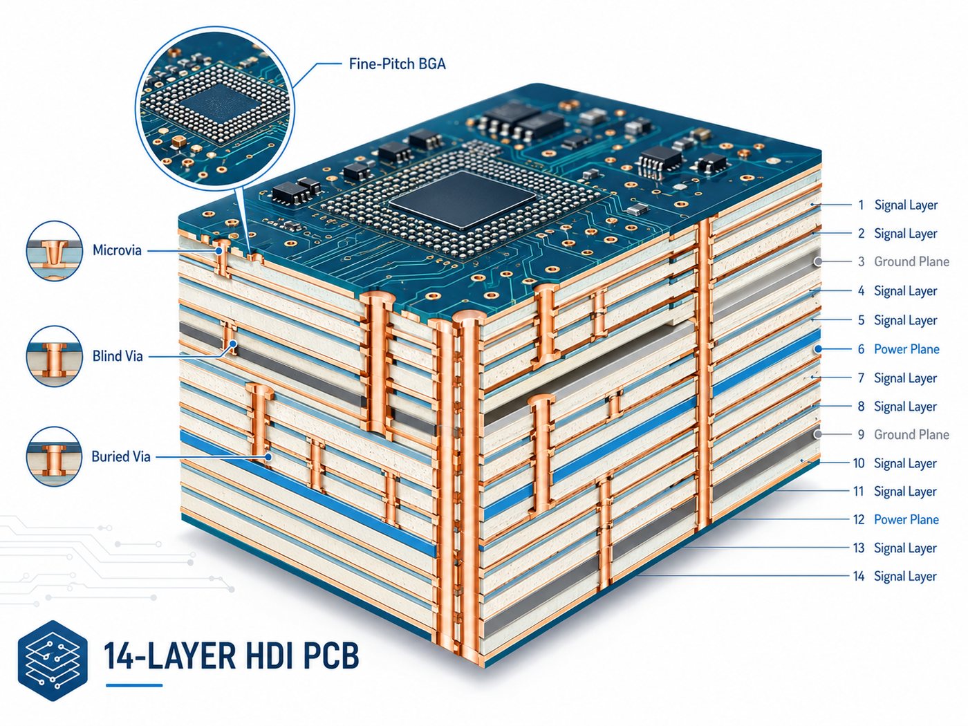
A 14-layer HDI PCB has 14 conductive copper layers and uses high-density vias to connect selected layers.
Common HDI features include:
- Laser-drilled microvias
- Blind and buried vias
- Via-in-pad
- Stacked or staggered microvias
- Sequential buildup layers
A conventional 14 layer PCB can also have 14 copper layers but rely mainly on through vias.
HDI becomes useful when a design needs more routing channels around fine-pitch BGAs, processors, FPGAs, or other dense packages. If component pitch is generous and board area is not constrained, a conventional multilayer board may be the more economical choice.
When Do You Need a 14-Layer HDI PCB?
A 14-layer HDI construction makes sense when routing density, board size, and electrical requirements begin competing for the same space.
Typical cases include:
- Fine-pitch BGA breakout
- High-I/O processors or FPGAs
- Compact communication or computing boards
- Multiple high-speed interfaces
- Designs requiring several continuous reference planes
- Dense layouts where through vias block inner-layer routing
HDI should solve a specific layout problem. If a standard 14-layer board can meet routing and electrical requirements without microvias or sequential buildup, adding HDI only increases fabrication complexity.
How Is a 14-Layer HDI PCB Stackup Designed?
A 14 layer PCB stackup should be built around routing, impedance, power distribution, board thickness, and via structure.
The HDI PCB stackup must be reviewed with the approved laminate system, finished thickness, copper distribution, and impedance targets before routing is released.
For a broader explanation of layer planning, see our PCB board stackup guide.
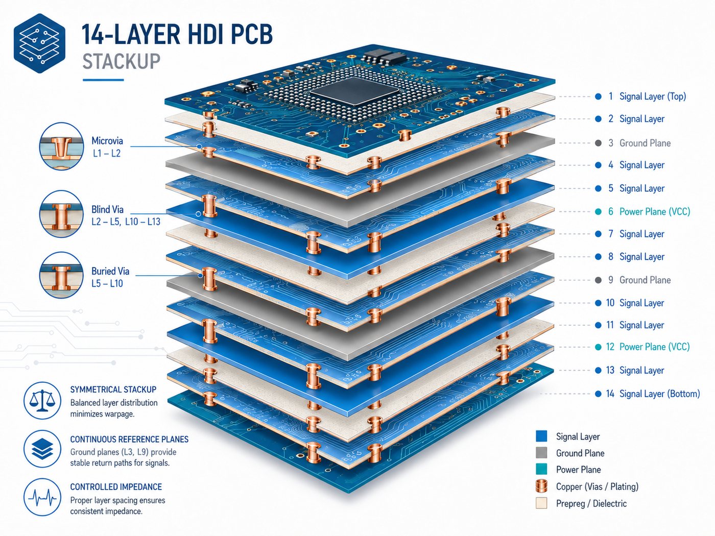
One possible arrangement is:
| Layer | Typical Function |
| L1 | Components / high-speed signal |
| L2 | Ground |
| L3 | High-speed signal |
| L4 | Ground |
| L5 | Signal |
| L6 | Power |
| L7 | Ground |
| L8 | Ground |
| L9 | Power |
| L10 | Signal |
| L11 | Ground |
| L12 | High-speed signal |
| L13 | Ground |
| L14 | Components / signal |
This is an example, not a universal stackup. Actual dielectric thickness, copper weight, and layer assignment depend on the design.
Three practical rules are useful:
- Keep high-speed signal layers next to continuous reference planes.
- Maintain a reasonably symmetrical construction to reduce warpage risk.
- Define the HDI layer stackup together with the microvia structure.
For example, if microvias connect L1-L2 and L2-L3, the dielectric thickness between those layers must suit the selected laser-via geometry. Stackup review should therefore happen before final routing.
Which HDI Buildup Structure Should a 14-Layer PCB Use?
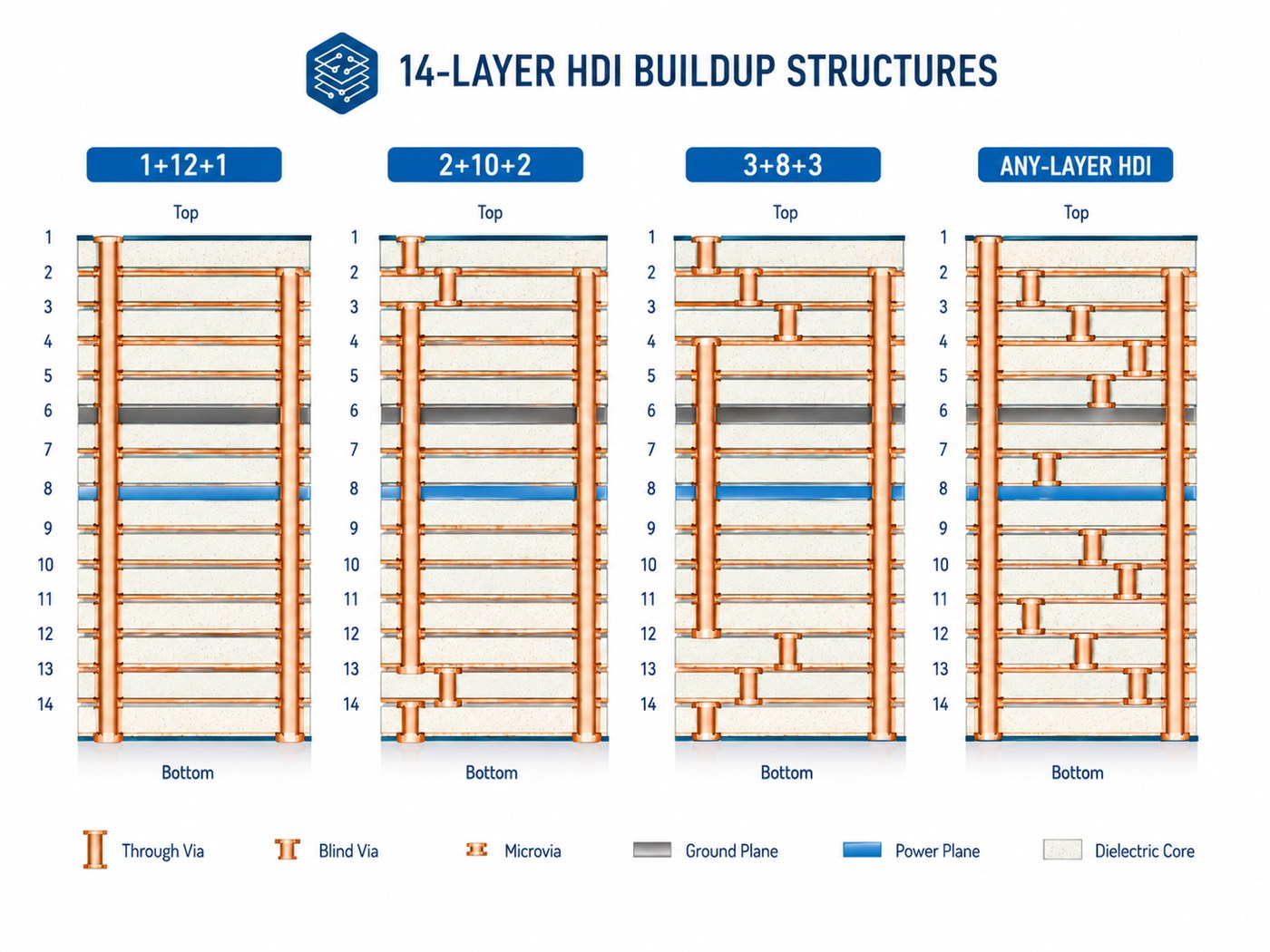
The buildup defines how many HDI layers are added around the central multilayer structure.
| Structure | Typical Use |
| 1+12+1 | Moderate-density outer-layer breakout |
| 2+10+2 | Higher-density BGA routing |
| 3+8+3 | Very dense component areas |
| Any-layer HDI | Designs requiring maximum interconnection flexibility |
A 1+12+1 structure is suitable when signals mainly need to move from the outer layer into the first internal routing layer.
A 2+10+2 structure provides more routing freedom around dense BGAs or processors.
Moving to 3-step or any-layer HDI should have a clear routing benefit. More buildup stages mean additional lamination, laser drilling, plating, filling, and registration control. The best structure is usually the simplest one that completes the routing without compromising electrical requirements.
How Should Microvias, Blind Vias, and Buried Vias Be Used?
Each via type has a different job.
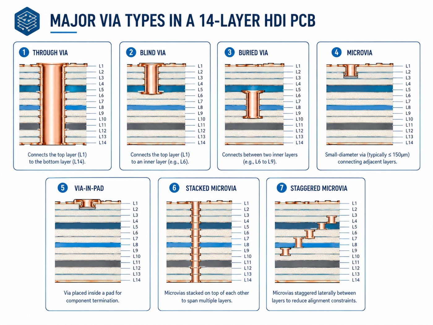
| Via Type | Best Use |
| Through via | General connections in lower-density areas |
| Blind via | Outer-to-inner layer connections |
| Buried via | Internal layer-to-layer routing |
| Microvia | Fine-pitch routing between nearby layers |
| Via-in-pad | BGA and small-package breakout |
| Stacked microvia | Maximum routing density |
| Staggered microvia | Multi-level routing where offset space is available |
Stacked microvias save space but require tighter control of:
- Copper filling
- Layer registration
- Plating quality
- Thermal reliability
Staggered microvias are often easier to manufacture when the layout has enough space for an offset transition.
Via-in-pad is useful under fine-pitch BGAs. These vias normally need to be filled and planarized so the component pad remains flat and solderable.
What Are the Key 14-Layer HDI PCB Design Rules?
These HDI PCB design guidelines should match the manufacturer’s actual production capability rather than a generic CAD rule set.
Confirm these items before layout is finalized:
- Microvia diameter and depth
- Capture-pad size
- Annular ring
- Minimum trace and space
- Via-to-pad clearance
- Via filling requirements
- Stacked microvia capability
- Layer registration tolerance
- Controlled impedance
Avoid using the factory’s absolute minimum geometry across the entire board. A feature that can be produced in a small isolated area may not be the best choice for stable volume production.
Copper balance should also be considered across the stack. Large differences in copper distribution between corresponding layers can increase warpage risk.
For controlled impedance, provide the target values and net types. Trace dimensions can then be adjusted against the actual laminate and finished dielectric thickness.
How Do You Control Signal and Power Integrity in a 14-Layer HDI PCB?
Fourteen layers provide useful flexibility for signal and power planning, but only if the reference structure is well organized.
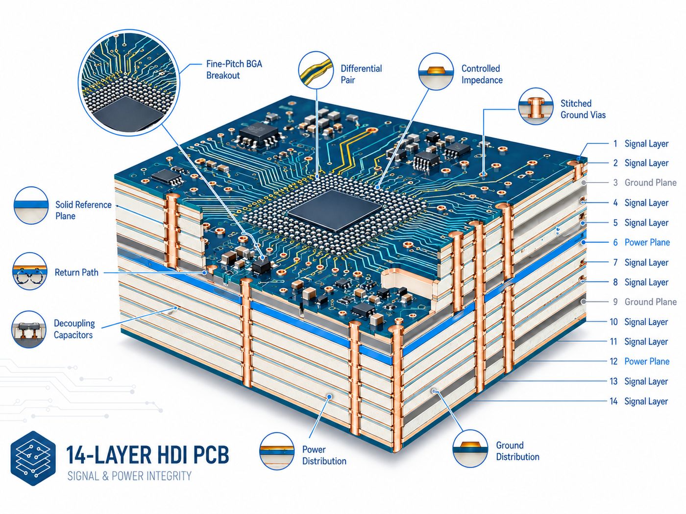
For signal integrity:
- Route high-speed traces next to solid reference planes.
- Avoid routing across plane splits.
- Keep differential-pair geometry consistent.
- Add nearby ground vias when signals change reference layers.
- Use short microvia transitions where appropriate.
- Avoid unnecessary through-via stubs.
For power integrity:
- Provide low-inductance paths between power and ground.
- Keep critical power planes close to their return planes where practical.
- Place decoupling close to high-current and fast-switching devices.
- Avoid fragmented return paths around plane cutouts.
The benefit of a 14-layer structure is not simply “more layers.” It is the ability to separate routing, reference, and power functions without forcing too many compromises.
Which Materials Are Suitable for a 14-Layer HDI PCB?
Material choice depends on electrical loss, thermal stress, and repeated-lamination requirements.
| Material Type | Typical Fit |
| High-Tg FR-4 | General industrial HDI |
| Low-loss FR-4 | Higher-speed digital designs |
| High-performance laminate | Demanding thermal or reliability requirements |
| Hybrid stackup | Designs where only selected layers need special properties |
Important parameters include:
- Tg
- Z-axis CTE
- Dk
- Df
- Resin system
- Moisture behavior
- Repeated-lamination performance
For high-speed designs, Dk and Df affect impedance and transmission loss. For multilayer HDI, Z-axis expansion and laminate stability also matter because vias experience repeated thermal stress during fabrication and assembly.
Material availability should be checked before quotation. An uncommon laminate can add unnecessary sourcing time even when the PCB design itself is straightforward.
How Is a 14-Layer HDI PCB Manufactured?
The HDI PCB manufacturing process for a 14-layer board adds sequential buildup steps to conventional multilayer fabrication.
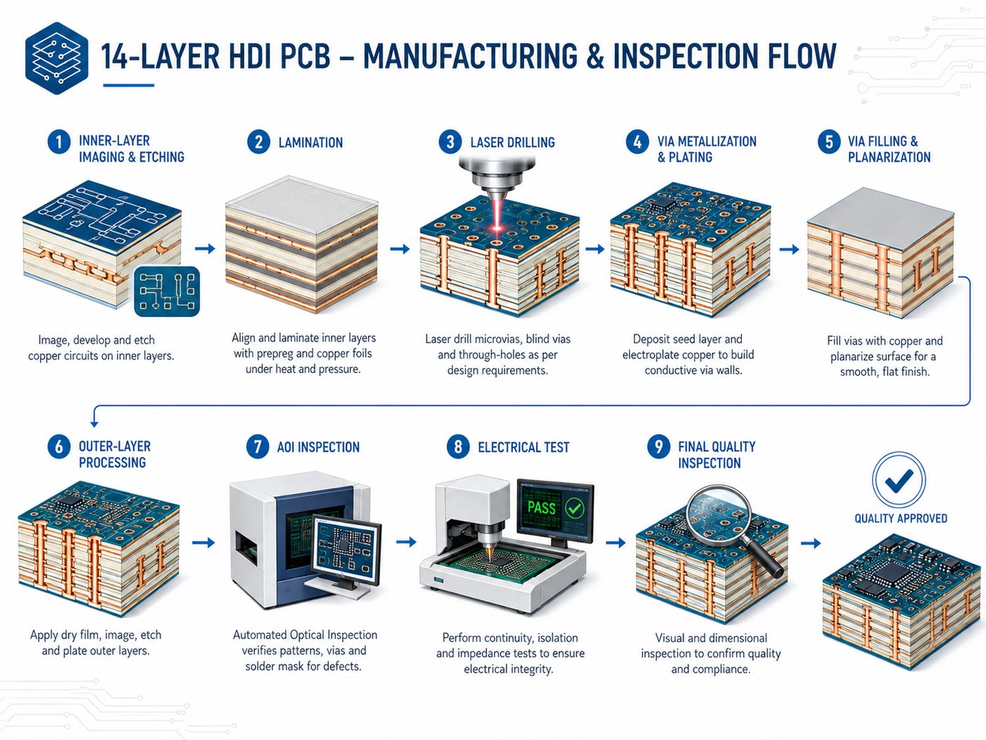
A simplified flow is:
- Inner-layer imaging and etching
- AOI inspection
- Core lamination
- Buried-via processing if required
- Buildup dielectric lamination
- Laser drilling
- Via metallization and plating
- Via filling and planarization where required
- Additional buildup cycles
- Outer-layer processing
- Solder mask and surface finish
- Electrical and final inspection
A 2+N+2 structure repeats the buildup and laser-drilling sequence for the second HDI level.
The main manufacturing challenge is maintaining alignment and via quality through repeated processing. A factory capable of standard 14-layer PCBs is therefore not automatically qualified for complex HDI builds.
How Is 14-Layer HDI PCB Reliability Verified?
Electrical testing confirms continuity, but HDI also requires inspection of internal interconnects.
Our broader PCB testing guide explains how electrical and inspection methods complement one another.
| Method | Main Purpose |
| AOI | Conductor and pattern inspection |
| Electrical test | Open and short detection |
| Microsection | Via plating, fill, and registration |
| Impedance coupon | Controlled impedance verification |
| X-ray | Selected internal structure inspection |
| Thermal testing | Interconnect behavior under temperature stress |
| Dimensional inspection | Alignment and finished geometry |
Microsection inspection is particularly useful for stacked or filled microvias because the critical structure is hidden inside the PCB.
For high-reliability projects, define acceptance class, coupon requirements, thermal testing, and reporting requirements at RFQ stage. These items can affect both panel design and quotation.
What Affects 14-Layer HDI PCB Cost and Lead Time?
HDI architecture often affects price more than the difference between conventional multilayer counts.
| Cost Driver | Why It Matters |
| Sequential lamination | Adds fabrication cycles |
| Stacked microvias | Requires tighter registration and filling control |
| Fine line/space | Reduces process margin |
| Via-in-pad filling | Adds filling and planarization |
| Specialty laminate | Raises material or sourcing cost |
| Tight impedance | Requires engineering and verification |
| Additional reliability tests | Adds inspection and qualification |
| Small prototype quantity | Setup cost is spread over fewer boards |
One effective way to control cost is to simplify the via structure.
If a 2+10+2 construction completes the routing, moving to 3+8+3 simply for extra flexibility is usually difficult to justify.
When comparing quotes, make sure each supplier is pricing the same material, stackup, microvia structure, surface finish, and testing requirements.
How Do You Choose a 14-Layer HDI PCB Manufacturer?
Do not qualify a supplier only by checking whether its capability table says “14 layers” or “HDI.”
Confirm the processes that your design actually requires:
- Sequential lamination
- Laser-drilled microvias
- Copper-filled via-in-pad
- Stacked or staggered microvias
- Fine line and space
- Controlled impedance
- Layer registration
- Microsection inspection
- Electrical testing
The manufacturer’s DFM feedback should also be specific. If an engineer suggests changing a stacked microvia to a staggered one, the reason should be clear—whether it is reliability, process margin, cost, or production capability.
For quotation, provide:
- Gerber or ODB++ data
- Drill files
- Preferred stackup, if available
- Material requirement
- Finished board thickness
- Copper weight
- Impedance requirements
- Microvia and via-in-pad details
- Surface finish
- Test requirements
- Prototype and production quantities
If the stackup is still open, provide the electrical and mechanical requirements instead.
At EBest Circuit, reviewing the stackup and via structure before layout is locked gives engineers more room to resolve manufacturing issues without forcing major redesign later.
Frequently Asked Questions About 14-Layer HDI PCBs
Is every 14-layer PCB an HDI PCB?
No. Fourteen layers describe the copper-layer count. HDI describes the interconnection technology. A 14-layer board can still be a conventional multilayer PCB.
What is a typical 14-layer HDI PCB stackup?
There is no universal stackup. Structures such as 1+12+1 and 2+10+2 are possible, but the final choice depends on BGA routing, impedance, board thickness, and required HDI layers.
What is the difference between a 14-layer HDI PCB and a standard 14-layer PCB?
A 14-layer HDI PCB uses localized high-density connections such as microvias and blind vias. A standard 14-layer PCB may rely mainly on through vias.
Should stacked or staggered microvias be used in a 14-layer HDI PCB?
Use stacked microvias when routing density requires vertical alignment. Use staggered microvias when enough offset space is available and the design does not require the more compact structure.
What files are required to manufacture a 14-layer HDI PCB?
Provide fabrication and drill data plus the stackup or electrical requirements, material, copper thickness, impedance targets, microvia details, via-fill requirements, surface finish, test requirements, and quantity.
How Can EBest Circuit Support Your 14-Layer HDI PCB Project?
At EBest Circuit, we support HDI PCB stackup review, DFM feedback, controlled impedance, laser-drilled microvias, and multilayer PCB fabrication. Send us your Gerber or ODB++ files, stackup, material, finished thickness, impedance targets, via structure, surface finish, test requirements, and quantities for an engineering review and quotation.
You may also like


Tags: 14 layer PCB stackup, 14-Layer HDI PCB, hdi pcb design guidelines, HDI PCB Manufacturing Process, hdi pcb stackup