





A voltage regulator PCB converts an available DC supply into a controlled rail for the load. The circuit may use a linear regulator, an LDO, a buck converter, a boost converter, or a buck-boost device. A correct schematic is only the starting point: capacitor behavior, switching-loop geometry, feedback routing, copper loss, and heat flow determine whether the assembled board remains stable under real operating conditions.
This guide follows the decisions in their practical order. It also uses one calculated example—a 12 V input and a 3.3 V, 0.30 A output—to show how requirements become component, layout, test, and manufacturing choices. The calculations are illustrative; they are not measured project results.
What Should Be Defined Before Designing a Voltage Regulator PCB?
Define the electrical limits, load behavior, environment, and acceptance tests before selecting the regulator. A nominal input voltage and a desired output voltage are not enough to approve a power design.
- Input range and source behavior: Record the minimum and maximum voltage at the board, not only the supply label. Include cable drop, battery discharge, adapter tolerance, input transients, and what happens when another load starts. The regulator must survive the maximum and continue regulating at the minimum.
- Output voltage and tolerance: Start with the powered device’s allowed range. Allocate that range among DC setpoint error, feedback-resistor tolerance, ripple, load transient, temperature drift, and voltage drop between the regulator and load.
- Continuous, peak, and transient current: State how much current the load draws, how quickly it changes, and how long peaks last. A 0.60 A pulse lasting microseconds presents a different capacitor and control-loop problem from a 0.60 A load held for minutes.
- Startup and sequencing: Define rise time, inrush limit, enable timing, pre-biased-output behavior, and the relationship to other rails. A rail can regulate correctly after startup yet violate a processor’s sequence requirement.
- Temperature and mechanical environment: Include ambient range, enclosure, airflow, nearby heat sources, available copper area, component height, and contact with other materials. These conditions affect both the IC and inductor.
- Acceptance method: Specify where voltage is measured, the load points, load-step profile, oscilloscope bandwidth, allowable ripple and transient excursion, and thermal operating point. Without a common method, two teams can report different results from the same board.
Example checkpoint: the running example fixes 12 V nominal input, 3.3 V output, and 0.30 A continuous load. Before release, a real product would still need its input extremes, transient profile, ambient limit, enclosure, ripple limit, and startup criteria. Leaving those fields open is safer than inventing universal values.
Which Voltage Regulator Topology Fits Your Power Requirements?
Choose the topology from the complete input range, output target, load current, allowable loss, and noise requirement. Package size or component count alone does not identify the lowest-risk solution.
| Topology | When it fits | Main PCB consequence | What must be checked |
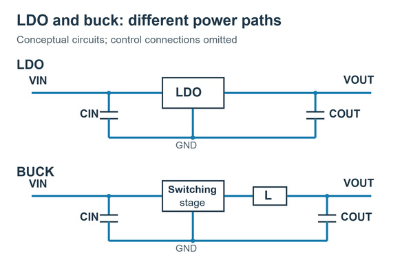
| Linear regulator or LDO | Input always exceeds output by the required headroom and the heat is manageable | No switching node; capacitor placement and thermal copper still matter | Dropout at peak load, dissipation, capacitor stability range, noise, and reverse-current behavior |
| Buck converter | Input remains above output | High-frequency input commutation loop, SW node, inductor, and output filter require controlled placement | Minimum on-time or duty behavior, efficiency across load, inductor current, ripple, EMI, and thermal limits |
| Boost converter | Input remains below output | The fast-changing power loop is concentrated around the switch, rectifier or synchronous device, and output capacitor | Startup, switch current, output disconnect behavior, and load transients |
| Buck-boost converter | Input can be above, below, or near output | More switching states and power paths make the reference layout especially important | Mode transitions, efficiency, ripple, component stress, and control behavior across the full input range |
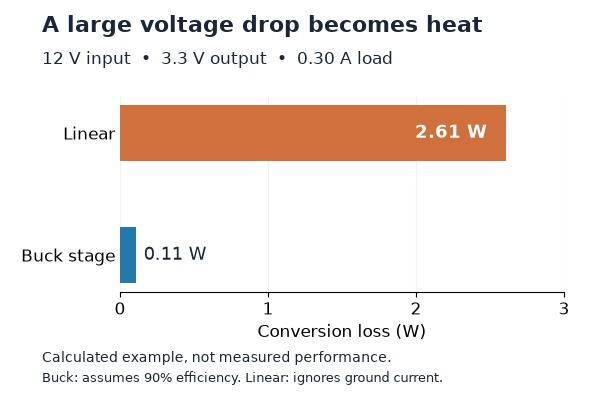
For the 12 V to 3.3 V, 0.30 A example, an LDO would dissipate approximately:
PLOSS = (12 V − 3.3 V) × 0.30 A = 2.61 W
The load receives 0.99 W. If a buck converter achieved an assumed 90% efficiency at that operating point, its estimated total loss would be:
PLOSS = (0.99 W ÷ 0.90) − 0.99 W ≈ 0.11 W
The 90% value is a screening assumption, not a guaranteed efficiency. It is still enough to show why a buck deserves evaluation before committing to an LDO. The selected device’s efficiency curves, switching mode, minimum load behavior, and thermal data must then be checked at the actual input, output, and current.
An integrated regulator module can reduce power-stage design work, but it is a packaging choice rather than a new conversion topology. Verify its external-capacitor needs, thermal derating, host-board copper, height, pinout, availability, and assembly requirements before substituting it for a controller-plus-passives design.
How Do You Select Capacitors, Inductors, and Feedback Components?
Begin with the exact regulator’s current datasheet and reference design, then validate each real part under bias, temperature, current, tolerance, and availability. Matching a printed capacitance or inductance value does not prove that a substitute behaves correctly in the circuit.
- Input capacitor: Check effective capacitance at the applied DC voltage, RMS ripple-current capability, voltage rating, temperature behavior, package parasitics, and the required proximity to VIN and power ground. A bulk capacitor near the connector does not replace the local high-frequency capacitor.
- Output capacitor: Stay within the regulator’s supported effective capacitance and ESR range. Verify the chosen part’s DC-bias curve and tolerance. X5R or X7R describes temperature characteristics; it does not guarantee how much capacitance remains at the operating voltage.
- Inductor: Check the converter’s supported inductance range, DC resistance, saturation current at peak inductor current, and thermal or RMS current at the expected load. Saturation current and temperature-rise current are different limits, so satisfying one does not automatically satisfy the other.
- Feedback network: Use the device equation and recommended resistor range. Include tolerance and bias-current error where relevant. Place the divider so that the high-impedance feedback node is short and protected from the switch node and inductor field.
- Optional filter or snubber: Add one only when a defined noise mechanism and a supported design method justify it. A ferrite bead, feed-forward capacitor, or RC snubber can introduce loss or resonance when copied without analysis.
- Critical BOM control: Record manufacturer part numbers for the regulator, capacitors, inductor, feedback parts, and other behavior-critical components. Define alternative approval by electrical characteristics, not package and nominal value alone.
For a device-specific starting point, the TI TPS62160 datasheet covers the example’s voltage and current and provides supported inductor and capacitor guidance. Its published design information includes 2.2 µH or 3.3 µH inductor options and a 22 µF nominal output-capacitor starting point for applicable conditions. Those values are not universal. The actual inductor current limits and the output capacitor’s effective value under bias still need part-level verification.
Example checkpoint: choose the final part numbers only after the product’s input extremes and transient requirement are known. If purchasing proposes a smaller ceramic capacitor with the same printed value, compare its DC-bias curve before approving the substitution.
How Should Components Be Placed Around a Voltage Regulator IC?
Place the components that carry fast-changing current first, following the selected regulator’s reference layout. A tidy schematic grouping does not guarantee a small electrical loop on the PCB.
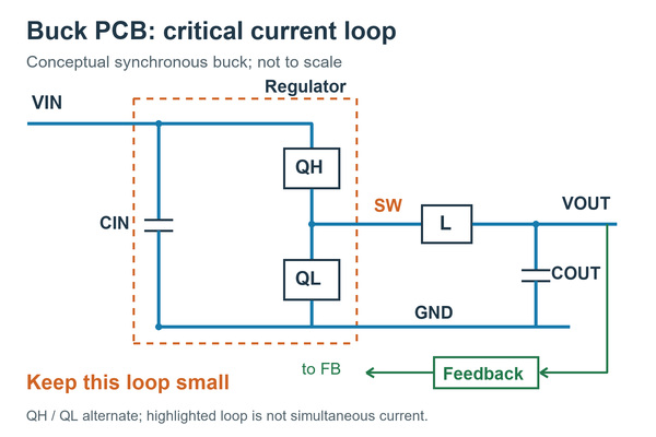
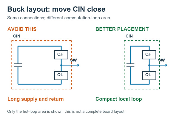
For a conventional synchronous buck, the input capacitor and the high-side and low-side switches form the high-frequency commutation loop, often called the hot loop. Parasitic inductance in this loop increases ringing and radiated or conducted noise. Analog Devices’ hot-loop layout discussion explains why capacitor, switch, and via placement must be considered as one current path.
Use this placement sequence:
- Place the local input ceramic capacitor at VIN and PGND. Make both connections short and direct. The observable result should be a compact path from the capacitor through the switching stage and back to the same capacitor.
- Place the inductor at the SW pin without enlarging the SW region. The connection must carry current, but unnecessary switch-node copper increases capacitive coupling. Review both copper area and proximity to feedback or other sensitive nets.
- Place the output capacitor at the inductor output and its return. Reserve physical access for a low-loop-area ripple measurement at the capacitor terminals.
- Place the feedback divider in the quiet region. Keep the divider midpoint close to FB and route the sense connection from the manufacturer-specified output point.
- Complete control and protection parts. Place bootstrap, compensation, soft-start, enable, and protection components according to the device’s application circuit. Do not let them displace the critical power loop.
The critical loop changes with topology. A boost converter usually prioritizes the loop through the switch, rectifier or synchronous device, and output capacitor. An LDO has no switching commutation loop, but it still needs compliant capacitors, a clean feedback path when adjustable, and a deliberate thermal path.
How Should Power, Ground, and Feedback Traces Be Routed?
Route the complete current and return paths first, then protect the feedback sense path from switching fields and shared voltage drop. A wide positive trace is not sufficient if the return path crosses a slot or necks through one via.
- VIN path: Review the path from connector to local input capacitor and regulator. Measurable input droop at the IC may come from a narrow trace, fuse, connector, or return path even when the bench supply reads 12 V.
- VOUT path: Size the path for allowable voltage drop and temperature rise. Inspect neck-downs at pads, connectors, layer transitions, and current-sense elements; the narrowest feature can dominate the loss.
- Ground return: Follow load current back to the input source. Maintain a continuous reference under sensitive signals and avoid forcing pulsed power current through the feedback divider’s ground reference.
- Feedback sense: Keep the high-impedance FB segment short and away from SW, the inductor, gate-drive paths, and other aggressors. Use the exact sense point shown by the device manufacturer, especially when a separate output-sense pin is provided.
- Layer changes: Evaluate outgoing and return vias together. Via count and geometry depend on copper thickness, plating, hole size, current, loss, reliability, and fabrication capability; there is no universal vias-per-amp rule.
- Remote load: Compare voltage at the output capacitor and at the load under the same current. If distribution loss matters, use supported remote sensing or change the copper path rather than raising the setpoint blindly.
For example, a complete supply-and-return resistance of 50 mΩ at 2 A causes 0.10 V drop and 0.20 W conductor loss. Although the running example carries only 0.30 A, the same method exposes connector or narrow-copper losses that a no-load reading misses.
Example checkpoint: review the 12 V input loop, the 3.3 V output path, and their returns as connected geometry. Then verify that the feedback sense point represents the voltage that must be regulated, not merely the most convenient pad.
How Can You Reduce Ripple, EMI, and Switching Noise?
Reduce noise at its source by controlling fast-current loops and switch-node coupling before adding filters. Layout-driven noise is difficult to remove with a larger capacitor placed far from the switching path.
- Minimize the commutation-loop area: Keep the input capacitor and switching-stage connections compact on the same layer where practical. If vias are unavoidable, place the outgoing and return transitions so the loop remains tight.
- Keep the switch node compact: Use enough copper for current and thermal needs without creating a large antenna-like region. Avoid routing feedback, clocks, sensor inputs, or external connectors beside or beneath it.
- Maintain a continuous reference: Do not cross plane gaps with sensitive or fast signals. A broken return path increases loop area and can convert common-mode disturbance into system-level EMI problems.
- Separate noisy and quiet placement zones: Keep the inductor and switching region away from analog inputs, oscillators, antennas, and high-impedance nodes. Separation works only when the return paths are also controlled.
- Investigate ringing before applying a remedy: Identify the ringing frequency, location, and current loop. If a supported snubber method is used, verify loss and behavior across input and load rather than tuning to one bench condition.
- Treat post-filters as systems: A ferrite bead and downstream capacitor can resonate and can change load-transient behavior. Check damping and ensure the filter does not violate the regulator’s feedback or output-capacitance requirements.
Example checkpoint: the calculated buck design should not be accepted because the DC output reads 3.3 V. Review the local input loop and SW node first, then confirm ripple and transients with a controlled measurement setup.
How Do You Prevent a Voltage Regulator PCB From Overheating?
Estimate loss by component, provide an intentional heat path into the PCB, and verify the assembled board in its real enclosure. The regulator IC is not always the hottest component; an inductor, diode, connector, or narrow copper region can set the thermal limit.
For a linear regulator, a first loss estimate is:
PLOSS ≈ (VIN − VOUT) × IOUT + VIN × IGND
When ground current is small, the simplified calculation for the running example is 2.61 W. A first junction estimate is sometimes written as:
TJ ≈ TA + PLOSS × θJA
This equation is a screening tool, not proof of final temperature. Texas Instruments’ semiconductor thermal-metrics guidance explains that θJA depends strongly on the board, test setup, copper, airflow, and environment; it is not a fixed package constant that can be transferred blindly to another PCB.
Use a thermal review with observable checks:
- Loss allocation: Estimate IC switching and conduction loss where the vendor provides a method, inductor copper and core loss, diode loss when applicable, and I²R loss in copper and connectors. Compare the estimate with measured input and output power on the assembled board.
- Package heat path: Implement the exposed pad, copper area, and thermal vias according to the selected package guidance. Confirm the pad’s required electrical net before copying a generic thermal pattern.
- Board spreading: Check whether plane cuts, solder-mask constraints, small islands, or dense neighboring parts reduce useful copper. More nominal copper does not help if heat cannot reach it.
- Inductor temperature: Compare peak current with saturation rating and RMS current with thermal rating, then measure the installed part. A converter can regulate while the inductor operates too hot.
- System condition: Test at the worst relevant input, load, ambient, airflow, orientation, and enclosure state. Record where temperature is measured and allow the assembly to approach thermal equilibrium.
Example checkpoint: the assumed 90%-efficient buck has about 0.11 W total calculated loss at the nominal point, far below the LDO’s 2.61 W screening result. That comparison supports the topology decision; it does not predict the assembled board’s junction or surface temperature.
How Do You Test Voltage Regulation Under Real Load Conditions?
Test the regulator at its input and load limits, measure both at the output capacitor and at the load, and document the probing method. A no-load multimeter check cannot validate ripple, transient response, distribution loss, startup, or thermal behavior.
- Verify safe power-off conditions. Check polarity, resistance to ground, fitted regulator and critical passive part numbers, and adjustable-divider values. Define a current-limited first-power setting. The expected result is no unexpected short or BOM mismatch before energy is applied.
- Check startup at controlled input. Monitor VIN, enable, VOUT, and input current. Observe rise time, overshoot, sequencing, and any restart. A clean final voltage does not erase a startup violation.
- Sweep static load and input. Measure VOUT at COUT and at the load from minimum to maximum operating current and at the defined input extremes. The difference between the two points reveals distribution loss.
- Apply defined load steps. Record starting current, ending current, transition rate, pulse duration, repetition, and measurement point. Compare excursion and recovery with the powered device’s allowed range.
- Measure ripple with a small probing loop. Probe directly across COUT with a ground spring or suitable tip-and-barrel connection and record oscilloscope bandwidth. Analog Devices’ AN-1144 shows how a long ground lead can create misleading spikes. If coax is used, apply the specified blocking and termination method rather than placing a bare 50 Ω load across the powered rail.
- Check operating modes and protection. Exercise light-load mode, enable cycling, startup with the expected load, current-limit behavior where safely defined, and relevant supply sequencing. Compare observations with the datasheet rather than assuming every change in switching pattern is instability.
- Run the thermal condition. Operate at the worst relevant input, load, ambient, airflow, and enclosure state. Record IC, inductor, connector, and hotspot temperatures together with the test condition.
Example checkpoint: the 12 V to 3.3 V design’s output is not declared good until it passes the product’s actual voltage, ripple, transient, startup, and thermal limits. This article defines the method but does not invent those acceptance values or results.
Why Does a Voltage Regulator PCB Oscillate, Overheat, or Drop Voltage?
Start with the symptom, measure the electrical event at the regulator and load, then change one suspected cause at a time. Replacing the IC first can hide a layout, component, source, or measurement problem without identifying it.
| Symptom | Likely cause | What to measure | Corrective action |
| Output falls as load rises | Input droop, dropout, current limit, or excessive path resistance | VIN at the IC, VOUT at COUT, VOUT at the load, input current, and enable during the same event | Correct source or path loss; select a regulator with adequate headroom/current only after the limiting mechanism is identified |
| COUT voltage is correct but load voltage is low | Resistive connector, narrow copper, return bottleneck, or inadequate vias | Differential drop along the positive and return paths at operating current | Widen or shorten the constrained path, improve the connection, or use supported remote sensing |
| Ripple appears excessive | Poor probing, insufficient effective capacitance, large hot loop, operating-mode behavior, or control issue | Repeat directly across COUT with a short ground; record bandwidth, load, VIN, switching behavior, and fitted capacitor | Fix the measurement setup first; then correct layout or component behavior and follow device stability guidance |
| Ringing follows a load step | Control response, resonant post-filter, parasitic loop, or unsuitable output network | Load current and VOUT on a common timebase; ringing frequency; capacitor and filter part numbers | Restore the supported output network, add justified damping, or use the manufacturer’s loop-assessment method |
| Output repeatedly stops after warming | Thermal protection, current limit, inductor heating, or input-source protection | IC and inductor temperature, VIN, VOUT, current, and restart timing | Reduce loss, improve the verified heat path, correct the overloaded component, or change topology/package |
| Output is higher than intended | Wrong divider value, open feedback path, incorrect sense point, or another source back-feeding the rail | With power removed, inspect parts and continuity; then monitor the rail under a current-limited safe startup | Correct the feedback network or power-path interaction before reconnecting sensitive loads |
| Output does not start | Missing input, inactive enable, excessive load, short, sequencing conflict, or unsupported pre-bias | VIN and enable at the pins, resistance to ground with power removed, VOUT rise, and input current | Correct the enable/sequence or fault; apply the manufacturer’s supported pre-bias and startup conditions |
| Sharp spikes change when the probe ground changes | Probe-loop pickup dominates the displayed waveform | Compare a long ground lead with a ground spring or controlled coax method at the same point | Use the documented low-loop-area method before modifying the PCB |
After a correction, repeat the exact startup, load, input, or thermal condition that exposed the fault. A waveform that changes because the probe or operating point changed is not evidence that the root cause was removed.
A Practical 12 V to 3.3 V Voltage Regulator PCB Example
This calculated example turns the earlier decisions into a reviewable design and test plan. It is based on published device guidance and explicit assumptions; it is not a measured customer board.
- Define the open requirements. The fixed values are 12 V nominal input, 3.3 V output, and 0.30 A continuous load. The project owner must still supply input extremes, transient current, ambient and enclosure conditions, ripple limit, startup behavior, and rail tolerance.
- Screen the topology. The load consumes 0.99 W. An LDO would dissipate about 2.61 W at nominal input, while a buck at an assumed 90% efficiency would lose about 0.11 W. Select a buck candidate for detailed evaluation.
- Choose a supported device and passives. TPS62160 is one published candidate whose input, output, and current range cover the example. Start from its current datasheet, supported inductor range, output-capacitor guidance, feedback arrangement, and reference layout. Confirm every final part under DC bias, peak/RMS current, temperature, and tolerance.
- Build the placement around the current loop. Place the local input ceramic beside VIN and PGND, keep the switching stage and SW node compact, place the inductor and output capacitor as shown by the reference layout, and reserve a quiet feedback region.
- Route the complete paths. Maintain continuous input, output, and return copper; remove pad or via bottlenecks; sense from the specified point; and keep feedback away from SW and the inductor.
- Review thermal and noise risks. Use loss estimates to identify likely hotspots, not to certify temperature. Inspect the package heat path, inductor rating, switch-node coupling, and nearby sensitive circuits.
- Create a measurable test plan. Check startup, input extremes, static loads, load steps, ripple at COUT with recorded bandwidth, voltage at the load, protection behavior where safe, and temperature in the final enclosure.
- Release controlled production data. Lock the board revision, stackup, critical BOM parts, thermal-pad and via treatment, inspection method where required, test points, programmed options, and pass/fail criteria.
The checkable output of the example is not a promised ripple number. It is a traceable chain from requirements to topology, selected device guidance, layout review, controlled BOM, and repeatable validation. A real voltage regulator PCB should replace every open assumption with its product-specific limit before production approval.
What Should Be Included for PCB Manufacturing and Assembly?
Release one consistent package that preserves the approved copper, stackup, critical components, assembly details, and powered test criteria. Manufacturing data should make substitutions and acceptance decisions visible instead of leaving them to interpretation.
- Current board identity: Provide matching Gerber or ODB++, drill, netlist, fabrication drawing, stackup, impedance information where applicable, assembly drawings, pick-and-place data, BOM, and revision. A mixed-revision package can invalidate the layout review even when each file opens correctly.
- Power-path construction: Transfer the approved copper weight, finished thickness assumptions, narrow current features, critical planes, and special via structures into the released fabrication drawing. The failure risk is excess loss after an unreviewed stackup or copper change; confirm the fabricator’s proposed construction against the electrical review.
- Thermal pad and via treatment: Define the exposed-pad geometry, electrical net, paste-aperture strategy, via fill or tenting requirement, and allowable changes in the released package. A generic pattern can cause solder loss or poor heat transfer, so require assembler and fabricator approval records for any deviation.
- Assembly and inspection: State polarity, orientation, moisture or handling controls when applicable, and inspection acceptance. AOI can inspect visible features; specify X-ray only when hidden-joint or underside-pad evidence is required by the package and acceptance plan. Record the inspection result so concealed solder defect risk is not inferred from a perimeter fillet.
- BOM substitution control: Mark critical regulator, capacitor, inductor, diode, MOSFET, and feedback parts in the released BOM. The failure risk from an unreviewed substitution includes changed stability, current, DC-bias capacitance, or thermal behavior; require technical approval and record the accepted alternative before placement.
- Test access and functional limits: Provide safe input, ground, enable, output, and load access in the approved test plan. State input range, load points, output limits, ripple method and bandwidth, startup or load-step requirement, and safe protection tests. This prevents a no-load reading from hiding a functional failure.
- Traceability: Tie the bare-board lot, assembly lot, BOM revision, programmed option, inspection record, and functional-test result to the same build identity when the product requires it. Verify that identity before shipment so a failure or identity mismatch can be contained without affecting unrelated builds.
The sequence should remain auditable: bare-board fabrication and electrical test, assembly and inspection, then the agreed powered checks. Any proposed stackup, copper, via, land-pattern, paste, or critical-BOM change should return for engineering review before production.
FAQs About Voltage Regulator PCB Design
Q1: Does every PCB need a local voltage regulator?
A1: No. A local regulator is needed only when the delivered rail cannot meet the load’s requirements. A board can use an already regulated source if the voltage at every load remains within its limits during startup, steady operation, and transients. Measure at the load before adding another stage.
Q2: Can a 5 V regulator produce 5 V from a 5 V supply?
A2: Not necessarily; the device still needs operating headroom. An LDO needs dropout headroom, while a buck has maximum-duty-cycle and operating limits near equal input and output voltages. Check the device at the minimum input reaching the pins. A buck-boost or another supply arrangement may be needed if the input crosses the output target.
Q3: Can the regulator be placed on the back of the PCB?
A3: Yes, if the critical electrical, thermal, and assembly geometry remains valid. Review the actual layer-changing paths for the required capacitors, current loops, heat flow, clearances, and probing access. Putting the IC underneath while leaving its local capacitor far away can create a poor high-frequency loop.
Q4: Does a ground plane solve all regulator return-path problems?
A4: No; a ground plane can still contain a poor return path. Slots, narrow bridges, shared pulsed-current paths, and badly placed vias can create voltage drop or coupling. Trace the return for each critical connection and inspect the continuous copper beneath sensitive routes.
Q5: Can two regulator outputs be connected in parallel for more current?
A5: Parallel outputs require a supported or validated current-sharing method. Small setpoint differences can make one device carry most of the load. Follow the manufacturer’s supported arrangement and verify sharing, startup, and protection; simply joining two outputs is not a reliable current upgrade.
Q6: What happens if the output is powered while the regulator input is off?
A6: The regulator may conduct reverse current unless it is designed to block it. USB, charged output capacitors, or another rail can create this condition. Check the datasheet’s reverse-current and sequencing behavior and add supported protection when the expected supply sequence requires it.
Q7: Why does switching ripple change at light load?
A7: Light-load control modes can change the switching pattern and ripple. Many converters enter pulse-skipping or another power-saving mode. Compare the observed behavior with the documented mode and the load’s noise limit before calling it instability.
Q8: Will a ferrite bead always make the output quieter?
A8: No; a ferrite bead can create a new resonance or transient problem. Bead impedance changes with frequency and DC current, while the downstream capacitor changes the network response. Check damping, loaded response, and the regulator’s output-network requirements, then repeat the same load-step and noise tests.
Q9: Which specification matters most for a battery-powered regulator?
A9: Evaluate total input energy across the product’s complete duty cycle. Quiescent current can dominate sleep, while conversion efficiency, divider current, shutdown current, and load duty cycle can dominate other states. Compare the actual sleep, wake, and active profile rather than selecting from one headline specification.
Q10: Can a pin-compatible regulator be substituted without retesting?
A10: No; pin compatibility does not establish electrical or thermal equivalence. Compare compensation, feedback reference, startup, current limit, switching mode, application circuits, and thermal behavior. Repeat the affected electrical and thermal tests before approving the BOM change.
Conclusion
A stable voltage regulator PCB comes from a connected decision process: define the rail and load, select a topology that fits the full operating range, verify real component behavior, control fast-current loops and feedback, estimate and measure heat, and release repeatable test criteria with the manufacturing data.
For a design or production review, send your Gerber or ODB++ files, stackup, BOM with critical manufacturer part numbers, quantity, and rail test requirements to sales@bestpcbs.com. EBest Circuit can provide a free DFM review and quote for the agreed fabrication and assembly scope. Electrical performance remains tied to the selected regulator guidance and the input, load, thermal, and measurement conditions defined for your product.
You may also like






Tags: voltage regulator module integration, voltage regulator PCB layout, voltage regulator ripple testing, voltage regulator thermal design