For PCB layout designers, hardware engineers, and DFM reviewers, a PCB acid trap can turn a small layout detail into a narrowed trace, irregular copper edge, or open circuit after etching. The practical task is to separate deep, restricted copper pockets from harmless corners, correct the geometry, and verify the exported manufacturing data. This guide moves from the failure mechanism and common risk locations through trace, pad, and copper-pour corrections to a final Gerber or ODB++ and fabricator DFM review.

What Are Acid Traps in PCB?
A PCB acid trap is a small, re-entrant region in copper geometry where etching may be less uniform than it is on open features. A classic example is a deep, narrow wedge between two copper edges. If that shape reduces local process margin, additional lateral etching can leave a conductor thinner than intended.
The term PCB acid trap is historical. PCB fabrication may use acidic or alkaline etchants, so the important issue is not whether the chemistry contains acid. The issue is whether the final copper pattern creates a tight pocket that is difficult to image, etch, rinse, and control consistently within the selected process.
Treat an acid trap as a manufacturability pattern, not as a label for every sharp-looking corner. Signal integrity, impedance discontinuities, current density, and return-path geometry are separate checks. A feature can be electrically acceptable but difficult to etch, or easy to manufacture but unsuitable for a high-speed electrical reason.
What Causes an Acid Trap During PCB Etching?
A PCB acid trap forms when restrictive copper geometry and the etching process combine to reduce local manufacturing margin. The main contributors are:
- Deep concave geometry: Two copper boundaries converge into a narrow pocket that is harder to image, expose to fresh chemistry, and reproduce than an open feature.
- Lateral etching: Etching removes copper sideways under the resist as well as through the exposed copper. A fine conductor beside the pocket can therefore finish narrower than the artwork.
- Process exposure: Older immersion processes were associated with retained or slowly exchanged etchant. Modern spray etching and tighter process control reduce that classic failure mode, but they do not make nearly closed pockets automatically safe.
- Limited feature margin: Thick copper, long etch time, tight line and space, imaging variation, and inadequate CAM compensation can make a marginal pocket more sensitive to edge loss.
No single angle proves that an acid trap will fail. Judge the complete pocket geometry together with copper thickness, nearby feature size, layer polarity, and the selected fabricator’s process capability.
Where Do Acid Traps Commonly Appear in PCB Layout?
A PCB acid trap most often appears where copper objects meet or where automated clearances reshape a pour. These transitions deserve more attention than an isolated, open trace bend because they can hide a narrow negative-space pocket in the rendered copper.
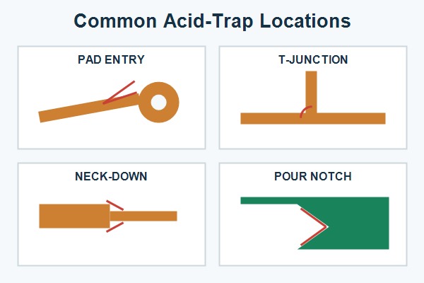
| Location | What to look for | Useful correction |
| Trace-to-pad entry | A thin triangular notch where a trace reaches a pad off-center or at a shallow angle | Move the entry point, align the trace, or use a controlled fillet or teardrop |
| T-junction or branch | A deep inside corner where a branch joins a wider conductor | Blend the junction or increase the open space around the branch |
| Neck-down transition | A concave wedge beside an abrupt width change near a pad or via | Lengthen the transition or move the width change away from the junction |
| Copper-pour boundary | A narrow bay, sliver, or nearly closed notch created by clearances and keepouts | Simplify the outline, enlarge the opening, or remove the isolated sliver |
| Thermal or plane cutout | A small pocket between spokes, pad clearance, and another copper edge | Adjust the thermal pattern or local clearance, then refill the pour |
Inspect the final copper boundary, not only the routing centerline. Pads, teardrops, thermal rules, keepouts, and polygon priorities can change the shape after routing. Refill all pours before deciding whether any of these locations is acceptable.
Why Do Acute Trace Angles Increase Acid Trap Risk?
An acute trace angle increases acid-trap risk when it creates a deep inside wedge with a narrow opening. That geometry combines a long concave edge, restricted fluid exchange, and a conductor whose local width may be sensitive to lateral etching.
The depth and openness of the wedge matter as much as the angle. A short, open 45-degree transition may offer more margin than a long notch formed by two shallow converging edges. Copper thickness and nearby minimum-width features also change the consequence of a small edge loss.
Use the angle as a screening clue, not as an acceptance limit. Inspect the rendered copper at each DRC or CAM coordinate. Reshape a deep pocket beside a critical trace; document an open feature that remains comfortably within the fabricator’s rules.
Are 90-Degree PCB Traces Actually Acid Traps?
No. A 90-degree PCB trace is not automatically an acid trap. A direction change with ample surrounding space is different from a narrow concave pocket created by overlapping traces, a trace-to-pad junction, or a pour clearance.
Using two 45-degree segments is a common routing convention because it avoids a sharp inside corner and often produces cleaner geometry. It does not fix every acid-trap condition. Replacing a right-angle bend while leaving a narrow notch beside a pad or copper pour is only a cosmetic change.
A layout can contain no obvious 90-degree bends and still have acid-trap risk at a shallow pad entry or nearly closed plane cutout. Apply broader PCB routing angle rules to electrical and layout decisions, but judge acid-trap risk from the final copper outline and manufacturing DFM result.
How Should You Route PCB Traces to Avoid Acid Traps?
Route traces with open inside corners and transitions that do not form long, narrow wedges. The objective is to remove restricted pockets while preserving clearance, impedance intent, current capacity, and component escape routing, not to force one bend style everywhere.
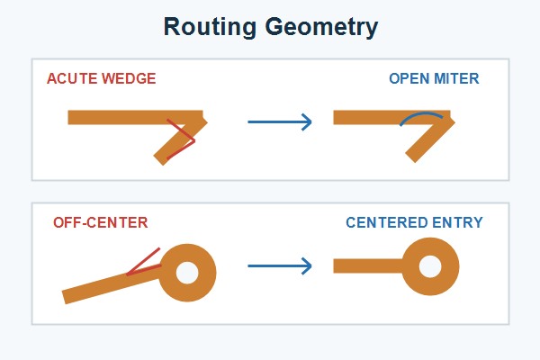
- Enter pads deliberately: Approach the pad near its centerline when practical. Check both sides of the junction for a triangular notch after the pad and trace shapes are combined.
- Use open bends: Prefer a mitered or smoothly curved route when an acute inside angle would otherwise form. The visible result should be an open concave boundary, not merely more segments.
- Separate width changes from junctions: Move a neck-down away from a pad, via, or branch when the combined transition creates a deep wedge.
- Blend branches with purpose: A controlled fillet can improve a T-junction, provided it does not reduce nearby spacing or create a copper sliver.
- Rerun electrical checks: After changing a controlled-impedance, high-current, differential, or timing-sensitive route, confirm that the manufacturing fix has not altered the electrical requirement.
A routing edit is complete only after the affected layer is refilled and replotted. The final copper should contain no restricted pocket and no new spacing, width, connectivity, or electrical violation.
How Should Copper Pours and Pad Connections Be Designed to Avoid Acid Traps?
Design copper pours and pad connections with simple, open boundaries that preserve the fabricator’s minimum feature and spacing margin. Review these four areas after every polygon refill:
- Copper-pour boundaries: Remove narrow bays and isolated slivers, enlarge the entrance to deep notches, and eliminate long slots created by overlapping keepouts.
- Polygon priorities: Check whether a higher-priority area reduces a lower-priority pour to a thin residual feature or nearly closed pocket.
- Pad and via entries: Avoid off-center trace entries that leave a triangular gap beside adjacent copper. Use a controlled teardrop or fillet only when it improves the transition without violating clearance.
- Thermals and high-voltage regions: Confirm that spokes, pad clearances, and added copper do not create a new concave pocket or reduce a required electrical spacing.
Accept the change only after refilling all zones and inspecting the exported positive and negative layers. The rendered manufacturing geometry, not the editable object before polygon processing, is the geometry that must pass.
How Do PCB Acid Traps Affect the Etching Process?
A PCB acid trap can reduce etching margin when a restricted pocket sits beside a feature that is already sensitive to edge loss. Etching removes copper vertically and laterally. Imaging, compensation, chemistry control, spray delivery, conveyor settings, and inspection help control that behavior, but a restricted pocket remains less forgiving than open geometry.
If the local process removes more copper than the artwork anticipated, the finished edge can recede into the protected conductor. The result may be an irregular notch or reduced trace width even when the rest of the panel is within tolerance. On negative artwork, the apparent pocket may represent clearance rather than copper, so layer polarity must be confirmed before interpreting the risk.
Review the feature against the exact copper weight, layer construction, and minimum line and space used for the build. Recheck geometry when the design moves to thicker copper, tighter spacing, or a different process. The wider PCB etching process also includes imaging, development, stripping, and inspection, all of which affect how faithfully artwork becomes finished copper.
Can PCB Acid Traps Cause Trace Necking or Open Circuits?
Yes. A PCB acid trap can contribute to trace necking and, in a severe case, an open circuit when local over-etching reaches the conductor. The consequence depends on nominal trace width, remaining copper, defect length, copper thickness, and the electrical role of the conductor.
Trace necking is a localized reduction in conductor width. It can increase resistance, reduce current-carrying margin, or create a weak point even when continuity remains. A complete open occurs when the etched region breaks the conductor. Fine traces near dense pads are more vulnerable because a small absolute edge loss consumes a larger share of their designed width.
Confirm the cause before assigning the failure to an acid trap. Misregistration, resist damage, scratches, contamination, and artwork defects can produce similar symptoms. Use the layer image, defect coordinates, available inspection or cross-section evidence, and the CAM report to connect the finished defect to the original geometry.
How Do PCB Manufacturing Capabilities Affect Acid Trap Risk?
The practical risk of a PCB acid trap depends on the margin available in the selected fabrication process. No universal minimum angle or pocket dimension guarantees the same result across different copper weights, layer densities, imaging systems, and etching lines.
- Copper thickness: Thicker copper generally requires more etching and changes the relationship between vertical and lateral removal. Confirm the finished copper target and compatible minimum line and spacing.
- Imaging resolution and registration: A narrow notch or sliver that is close to the imaging limit has less tolerance for artwork and process variation.
- Etching equipment and control: Chemistry, spray delivery, compensation, conveyor control, and inspection affect how consistently dense and isolated features are reproduced.
- Layer polarity and density: Positive and negative layers can reverse the meaning of a narrow region, while dense copper patterns interact differently from isolated features.
- CAM and DFM rules: Detection names and thresholds vary. The useful output is a coordinate-specific disposition tied to the supplied stackup and copper specification.
Send any feature near a stated limit to the selected fabricator for a coordinate-specific decision. Ask whether it is acceptable as drawn, requires CAM compensation, or should be modified, then record the answer against the exact layer and coordinates.
How Should You Check a PCB Design for Acid Traps Before Manufacturing?
Check suspected acid traps in the final manufacturing data, not only in the editable PCB layout. Each step below produces an observable result tied to the file set that will actually be quoted and built.
- Refill copper and run the native DRC. Resolve acute-angle, sliver, minimum-width, spacing, and unconnected-copper findings. The output should be a saved board state with no unexplained relevant violations.
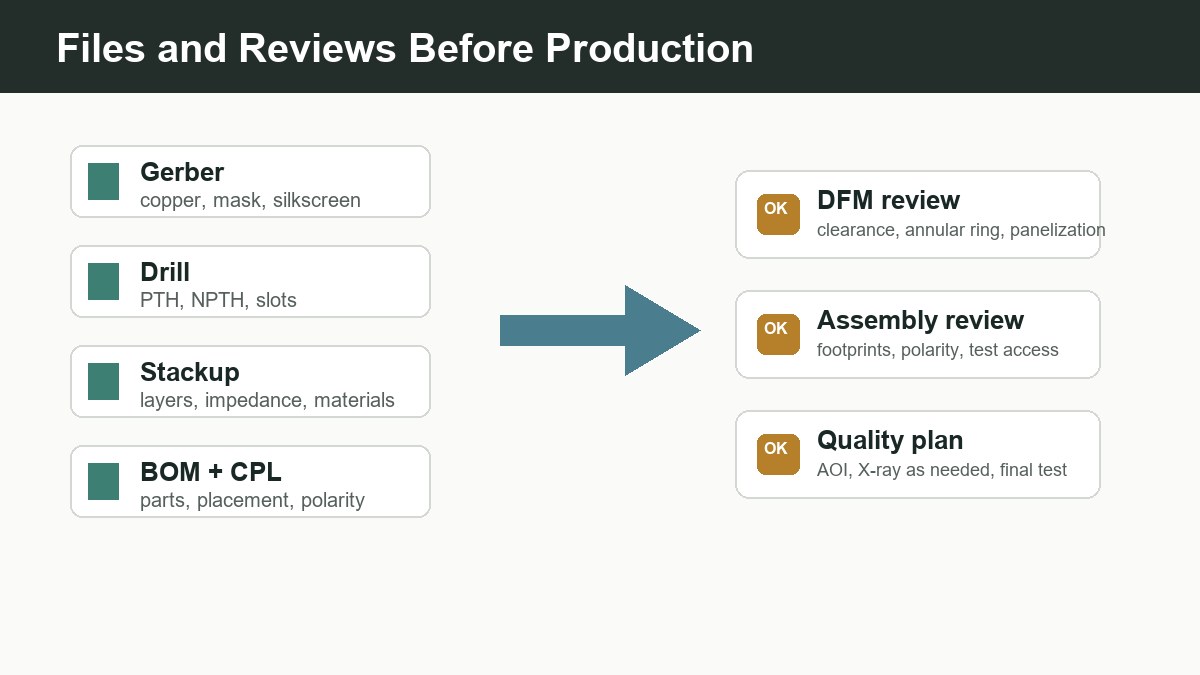
- Generate the actual release package. Export Gerber or ODB++ with the same layer, polarity, aperture, and scaling settings intended for the fabricator. The output should be the dated package that will be quoted and built.
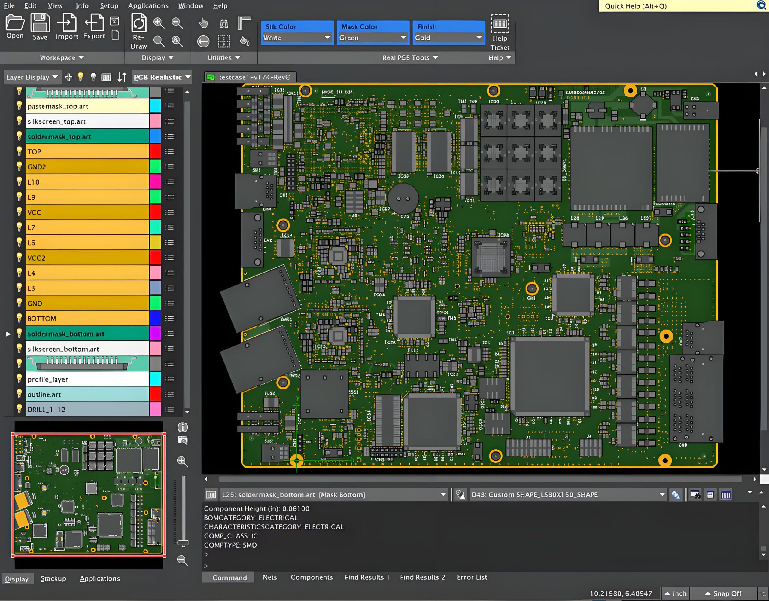
- Open the package in an independent viewer. Confirm layer names, polarity, alignment, scale, and copper presence. This separates source-editor display assumptions from the plotted result.
- Inspect known risk locations at high zoom. Check trace-to-pad entries, T-junctions, neck-downs, thermal features, plane cutouts, and pour notches. Record the layer and coordinates of each questionable pocket.
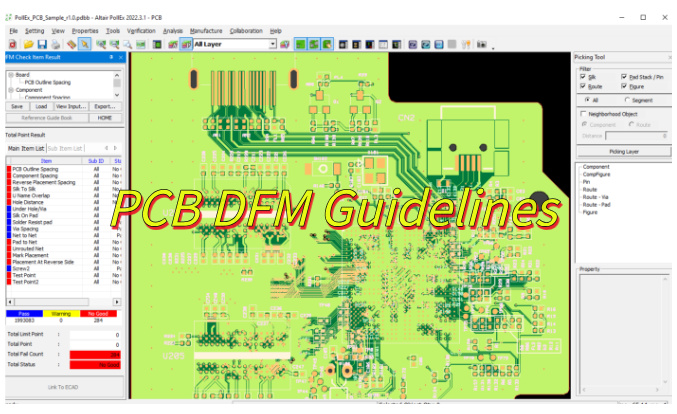
- Run a fabrication-oriented DFM analysis. Review acid-trap or acute-angle flags together with minimum feature, spacing, sliver, annular-ring, drill, and solder-mask results. Each flag should end with a correction or a documented disposition.
- Request a fabricator review for borderline features. Provide the final files, stackup, finished copper requirement, minimum line and spacing, and marked coordinates. The expected output is an order-specific accept, compensate, or modify decision.
- Replot after any correction. Repeat the independent viewer and DFM checks on the revised package. Only the final exported hash and file set should be released.
A clean CAD screen is not release evidence if the pour was not refilled or the exported artwork changed afterward. Keep the final file hash, DRC and DFM reports, and accepted exceptions together so later revisions can be compared with the approved manufacturing data.
FAQs About PCB Acid Traps
Acid-trap decisions depend on final copper geometry and process evidence, not on the etchant name, the presence of a teardrop, or the presence of a via alone.
Q1: What is the difference between an acid trap and a copper sliver?
A1: An acid trap describes a restricted concave geometry, while a copper sliver is a very narrow residual piece of copper. The same layout interaction can create both, but they are checked differently. Inspect the pocket that may affect etching and the remaining copper feature that may be too narrow to reproduce reliably.
Q2: Does an alkaline etching process eliminate acid traps?
A2: No. “Acid trap” is a historical term. An alkaline process may change the chemistry and control window, but tight concave geometry can still reduce process margin. Use the fabricator’s DFM rules for the actual process.
Q3: Do teardrops always prevent acid traps at pads and vias?
A3: No. A well-proportioned teardrop can smooth a trace-to-pad transition, but an oversized or poorly placed teardrop can create a new clearance or concave-geometry problem. Refill the copper and inspect both sides of the connection.
Q4: Can a via create a PCB acid trap?
A4: The via itself is not automatically an acid trap, but the surrounding copper geometry can create one. Check the trace entry, thermal spokes, pad clearance, nearby pour boundary, and any teardrop in the final layer artwork.
Q5: What should you send a manufacturer to review a suspected acid trap?
A5: Send the final Gerber or ODB++ package, stackup, finished copper requirement, minimum line and spacing, and the exact layer and coordinates. Include a marked image of the feature and any proposed correction. This gives CAM engineering enough context to return a specific manufacturability disposition.
For every uncertain feature, the useful result is a coordinate-specific accept, compensate, or modify decision based on the final release data.
Conclusion
Treat a PCB acid trap as a geometry-and-process risk, not as a simple angle violation. Correct deep or nearly closed copper pockets wherever they reduce etching margin, especially at trace-to-pad entries, branches, neck-downs, thermal clearances, and pour boundaries. A 90-degree bend with open surrounding geometry is not automatically defective; the final copper outline and the selected fabricator’s process capability determine whether it is acceptable.
Release the design only after refilling every pour, exporting the final Gerber or ODB++ package, and giving each relevant DFM flag a coordinate-specific disposition. If a borderline PCB acid trap remains, send the layer, coordinates, stackup, finished copper requirement, and marked final files to sales@bestpcbs.com. This gives CAM engineering the information needed to accept the feature, compensate it, or request a design change before fabrication.