





IPC-7351 provides a method for developing surface-mount land patterns from component dimensions, tolerances and solder-joint goals. The useful result is a set of copper pads that accommodates the intended terminals and assembly process. A package label such as 0603 or QFN-32 is only the starting point: it does not supply all the dimensions needed to draw those pads.
A practical footprint design connects the package drawing to pad geometry, placement space and manufacturing outputs. The sequence below follows that connection, including a real 0603 resistor example that turns a manufacturer’s recommended land pattern into CAD pad sizes and coordinates.
What Is IPC-7351, and Which Version Applies?
IPC-7351 covers land patterns for surface-mount components. Its method relates terminal geometry and dimensional variation to the solder connection. This makes it useful when building a footprint library, comparing an imported footprint with a component drawing, or reviewing a package substitution.
The official IPC revision table, checked on August 31, 2026, lists IPC-7351B from June 2010 and marks it as no longer maintained. It also lists IPC-7352, Generic Guideline for Land Pattern Design, from 2023, covering surface-mount and through-hole land patterns. Review that newer guidance for new library work; retain the specified edition for an existing design rather than silently changing its basis.
IPC-7351 succeeded IPC-SM-782. Broader board design, stencil design and soldered-assembly requirements are addressed separately by the IPC-2220 series, IPC-7525 and J-STD-001. They support different release decisions and do not replace the land-pattern calculation.
What Is Included in an IPC-7351 Land Pattern?
A land pattern primarily defines the copper lands and their geometric relationship to the component terminals. A complete PCB footprint also carries the mask, paste, courtyard, assembly outline and orientation information needed to use that geometry in a board design.
| Footprint information | What the designer must establish |
|---|---|
| Copper lands | Pad width, length, spacing and terminal numbering |
| Solder-mask openings | Exposed copper and the permitted registration allowance |
| Paste apertures | The stencil openings required for the chosen solder deposit |
| Courtyard | A placement boundary around the component and land-pattern envelope |
| Assembly outline and orientation | Body location, pin-1 reference, origin and rotation convention |
An IPC-7351 land pattern becomes a usable library footprint when these outputs agree. For example, a QFN’s copper thermal pad, its segmented paste openings and its courtyard have different jobs; changing one does not automatically define the other two.
Which Component Dimensions Are Required Before Pad Design?
Extract the dimensions of the solderable terminals, not just the package body. Work from the exact manufacturer part number and drawing revision, and preserve the drawing’s top-view or bottom-view designation.
- Terminal width: find the minimum and maximum width of each solderable lead or electrode. This controls the transverse pad width and side-joint allowance; body width is not a substitute for a narrow lead.
- Terminal length: record the solderable length and its limits. For opposing terminals, it helps establish the gap between their inner edges and the available heel connection.
- Lead span: locate the outside-to-outside terminal dimension. On a gull-wing package this extends beyond the molded body; using body length here would shorten the calculated outer land span.
- Pitch: identify the center-to-center terminal spacing. Check adjacent copper after calculating pad width, because a suitable side allowance on one lead may leave inadequate separation from its neighbor.
- Body dimensions and height: retain their limits for courtyard, silkscreen and mechanical checks. These dimensions describe placement space, while terminal geometry determines the solder connection.
- Exposed-pad dimensions: capture the center pad, its location and its electrical assignment. Check whether it has a separate terminal number and a device-specific paste or via recommendation.
- Minimum and maximum limits: convert each tolerance explicitly. A dimension of 0.40 ± 0.05 mm has limits of 0.35 and 0.45 mm and a total range of 0.10 mm; entering 0.05 as the full range changes the calculation.
Where a calculator requests fabrication and placement tolerances, use the definitions required by that tool’s method. A plus/minus coordinate accuracy, a total tolerance range and a true-position diameter are not interchangeable inputs.
How Do You Calculate an IPC-7351 Land Pattern?
Start with terminal limits, select the solder-joint goals and combine the relevant component, fabrication and placement tolerances. For an opposing-terminal pattern, the main outputs are the outer land span Z, inner gap G and land width X. These describe the copper arrangement rather than the body outline.
| Output | Geometric meaning | Main joint relationship |
|---|---|---|
| Z | Outside edge to outside edge of opposing lands | Toe allowance beyond the terminal ends |
| G | Clear gap between the inner land edges | Heel allowance toward the package center |
| X | Width of one land across the terminal | Side allowance beside the terminal |
Toe, heel and side joint goals control different land edges: increasing the toe goal generally extends Z; increasing the heel goal generally reduces G; increasing the side goal generally widens X. The selected component-family method determines the actual values, signs and tolerance treatment. A gull-wing heel goal should not be transferred to a chip termination or BGA ball.
The calculation path is: drawing limits → family and density choice → joint goals and process tolerances → Z, G and X → individual pads. Check the resulting copper against the terminal extremes, then against neighboring pads and the intended assembly process.
For the IPC presentation’s opposing-terminal outer-span model, the relationship can be written as:
Z = Lmin + 2JT + R
R = √(C² + F² + P²)
Here Lmin is the minimum outer terminal span, JT is the toe goal, C is the component span tolerance, F is fabrication tolerance and P is placement tolerance, expressed in that model’s conventions. The root-sum-square term combines variation; it is not another fillet goal. G and X use their corresponding terminal dimensions and heel/side goals.
For two equal rectangular lands centered symmetrically about the origin, the last step is simple geometry:
Pad length Y = (Z − G) / 2
Pad-center distance = (Z + G) / 2
Each center lies at ±(Z + G)/4 along the component’s length axis, and each land has width X. These relationships convert an already selected land pattern into CAD objects; they do not determine the joint goals or replace the tolerance calculation. The real resistor example below uses this conversion with manufacturer-recommended dimensions.
How Do You Choose IPC-7351 Density Levels A, B and C?
Select the density level by balancing the joint geometry, placement space and process capability. Within a supported component family, the three choices generally move from more generous to more compact land patterns and courtyard allowances. The amount of that change is family-dependent; it is not a single scale factor applied to every pad.
| Level | Lands | Courtyard allowance | Selection context |
|---|---|---|---|
| A — Maximum | More generous | Typically larger | Extra assembly or service space where the process benefits |
| B — Nominal | Medium | Typically medium | An initial choice for a documented general assembly process |
| C — Least | More compact | Typically smaller | Tight layouts with a proven process |
- Level A: compare the additional copper and placement area with the actual soldering and service needs. Extra allowance can improve access, but a courtyard alone does not prove that a rework nozzle will fit or that the larger paste deposit is suitable.
- Level B: use the nominal family targets as a starting point, then compare the result with the manufacturer’s attachment recommendation. A default selection is useful only when its underlying tolerances match the intended process.
- Level C: examine the smallest pad gaps, mask webs, paste apertures and available placement margin before committing to the compact option. If the fabricator or assembler cannot support those features, change the footprint choice or placement rather than suppressing the design-rule warning.
IPC-7351 density levels are not IPC product Classes 1, 2 and 3. Neither a Level A footprint nor a larger courtyard establishes an assembly’s reliability classification.
How Do You Use an IPC-7351 Land Pattern Calculator?
Enter component and process data, generate the geometry, then compare the exported result with the package recommendation. An IPC-7351 land pattern calculator is most useful when its inputs and outputs remain visible and reviewable.
- Select the component family and method. Choose the actual terminal structure, such as chip, gull-wing or QFN, and record the implemented standard revision. The input diagram should match the package drawing.
- Enter the dimensional limits. Supply pitch, terminal width and length, outside span, body dimensions and any exposed pad. Verify the units and the meaning of every min/max field before generating a preview.
- Set density and process inputs. Choose the family-specific joint goals and supported fabrication and placement tolerances. Save those settings with the footprint so a later reviewer can reproduce the result.
- Read the generated outputs. Check pad width and length, inner gap, overall span and courtyard; inspect the name, numbering, origin and any optional mask or paste layers. Some tools generate more of these objects than others.
- Compare and export. Overlay the copper with the manufacturer’s recommended footprint and investigate differences. Reopen the exported CAD footprint to confirm that its pad geometry and layer assignments match the reviewed preview.
Before using an older IPC-7351 land pattern viewer, check its supported standard revision and export features. A working preview does not establish that the tool is current or supported.
How Is an IPC-7351 Courtyard Defined and Sized?
A courtyard is a library placement boundary used to check a component against its neighbors. It supports placement DRC and assembly-space planning by enclosing the relevant component and land-pattern envelope with an added allowance.
Establish the controlling boundary in each direction: leads or copper lands may extend beyond the body. Apply the documented component-family and density-level allowance outside that envelope. Library conventions can differ in their dimensional basis and rounding, so compare an imported courtyard with its source method before adjusting it.
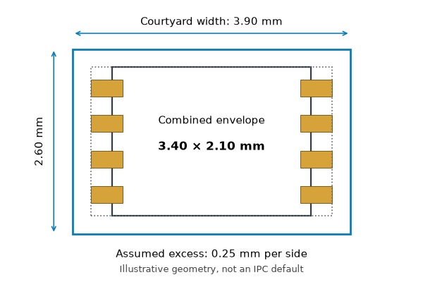
For an illustrative geometric example, not an IPC default, take a 3.40 × 2.10 mm controlling envelope and an agreed excess of 0.25 mm per side:
Width = 3.40 + 2(0.25) = 3.90 mm
Height = 2.10 + 2(0.25) = 2.60 mm
Place that boundary on the CAD courtyard layer and run placement checks on the actual board. Investigate overlaps against the assembly plan; do not shrink the whole library to make warnings disappear. Additional rework or electrical spacing belongs in separate constraints.
How Much Component Spacing Is Required Beyond the Courtyard?
There is no single IPC-7351 component spacing value suitable for every package and assembly process. Courtyard checks answer one placement question; they do not replace copper, insulation or tool-access checks.
| Check | What controls it |
|---|---|
| Courtyard separation | The selected land-pattern method and library allowance |
| Copper spacing | Actual copper edges, electrical requirements and fabrication capability |
| Creepage and clearance | Working voltage, insulation system, environment and applicable product requirements |
| Assembly access | Placement equipment, neighboring component shapes and the SMT process |
| Rework access | Package removal method, tooling and nearby heat-sensitive parts |
If two facing courtyards each include 0.25 mm beyond their underlying envelopes and their boundaries touch, the example produces a 0.50 mm envelope gap. That does not make 0.50 mm a universal body gap or an approved rework clearance. Measure each required separation between the physical features to which that requirement applies.
For a dense area, review the limiting pair of components with the assembler. A local, documented exception can preserve useful DRC elsewhere; a global reduction removes the warning from unrelated placements as well.
How Does IPC-7351 Apply to 0402 and 0603 Components?
There is no universal IPC-7351 pad size for every 0402 or 0603 part. Terminal construction and dimensional limits can differ between resistor, capacitor and inductor families, even when their nominal body sizes match.
First resolve the size-code system. These are common nominal body-size families, not pad dimensions:
| Imperial code | Metric code | Nominal body size |
|---|---|---|
| 0201 | 0603 | 0.6 × 0.3 mm |
| 0402 | 1005 | 1.0 × 0.5 mm |
| 0603 | 1608 | 1.6 × 0.8 mm |
Consider the actual Vishay D11/CRCW0603 e3 package. Its D/CRCW e3 datasheet, revision 14-Apr-2026, page 11, gives L = 1.55 +0.10/−0.05 mm, W = 0.85 ±0.10 mm, H = 0.45 ±0.05 mm and T1/T2 = 0.30 ±0.20 mm. Thus L spans 1.50–1.65 mm, while each termination-length limit spans 0.10–0.50 mm.
The same page recommends this reflow land pattern: G = 0.75 mm, Y = 0.75 mm, X = 1.00 mm and Z = 2.25 mm. It references IPC-7351 among its design considerations; it does not identify these values as a particular density-level calculation.
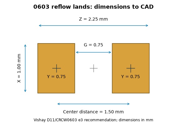
To draw that pattern in CAD:
- Create two rectangular copper lands. Set length along the component axis to 0.75 mm and transverse width to 1.00 mm.
- Place their centers at (−0.75, 0) and (+0.75, 0) mm. The resulting center distance is 1.50 mm.
- Measure the finished geometry. The inner gap is 1.50 − 0.75 = 0.75 mm; the outer span is 1.50 + 0.75 = 2.25 mm.
This is a manufacturer-recommended reflow example, not a reconstructed IPC calculation with invented fabrication, placement or fillet inputs. To generate a different density variant, enter the actual terminal limits and agreed process assumptions into the selected method, then compare its Z/G/X outputs with this reference. Record why any difference is accepted.
For a chip capacitor, balanced land geometry and paste deposition help limit unequal wetting forces that can cause tombstoning during reflow. For an inductor, verify where its electrodes are exposed before reusing a same-size capacitor footprint; the body outline alone cannot establish the solder connection.
How Do You Design an IPC-7351 Land Pattern for QFN Packages?
Design the perimeter connection and exposed center-pad attachment as separate, coordinated features. Use the exact device drawing to establish terminal pitch, width, length, pullback and exposed-pad geometry before selecting a generic QFN calculation.
- Perimeter lands: match pad numbering and the terminal extents, then inspect neighboring copper and mask gaps. Whether the package has solder-wettable flanks affects what a side fillet or visual inspection can establish.
- Exposed pad: follow the specified electrical connection and thermal layout. Confirm pad number, dimensions and location; a generic QFN outline does not establish the center pad’s net or the via arrangement.
- Paste apertures: coordinate segmentation, stencil thickness and the intended solder volume. Excess solder under the center can lift the package and compromise perimeter joints. TI’s QFN and SON attachment guide discusses approximately 50%–70% paste-area coverage in its stated context; this is not a universal copper-pad reduction.
- Thermal vias: specify their construction together with the stencil design. Open vias can remove solder from the joint area, so review via treatment and paste loss before releasing fabrication files.
The review should produce consistent copper, mask and paste layers, plus an agreed via specification. For a new assembly process, define how the hidden center joint and perimeter connections will be inspected or evaluated; visible outside edges do not reveal the entire attachment.
How Do You Design an IPC-7351 Land Pattern for BGA Packages?
Begin with the device’s ball map and PCB attachment recommendation, then fit the escape routing around the approved lands. Ball pitch alone does not define copper diameter, populated positions or mask openings.
- Match the physical array. Check ball diameter, pitch, row/column labels and intentionally absent positions. The populated ball map must agree with the schematic-to-pad mapping.
- Select the land and mask construction. With NSMD pads, the mask opening is larger than the copper land. With SMD pads, the mask opening defines the exposed solderable area. TI’s WCSP guidance favors NSMD in that context, but NSMD is not a blanket requirement for every BGA; use the specific device recommendation.
- Prove the escape geometry. Compare pad diameter, trace width, clearance, via size and the proposed layer structure. If a route cannot fit between lands, reassess the routing and fabrication options before reducing approved pads merely to make space.
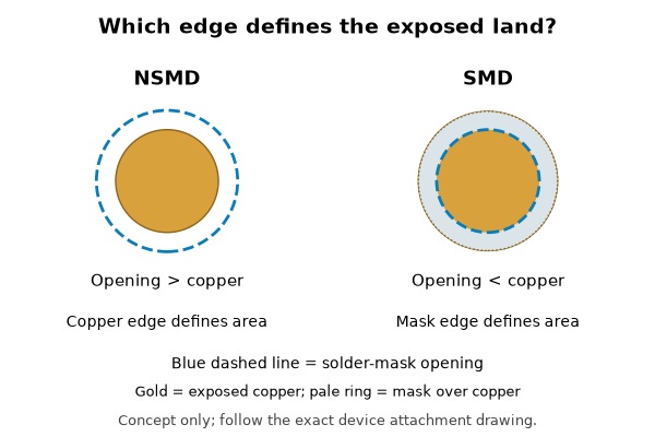
Mask definition is a separate classification from QFN or BGA terminal construction. Keep those decisions separate in the library record, and use the device’s orientation drawing to confirm A1 before exporting placement data.
How Does the IPC-7351 Naming Convention Work?
A footprint name encodes package characteristics so similar-looking geometries can be distinguished. The exact fields depend on the family and the naming implementation. Read a name with its convention, rather than assuming every CAD library uses the same string format.
For example, SOT23-95P280X110-5N encodes a SOT23-family package using these fields:
| Code element | Meaning in this example |
|---|---|
| SOT23 | Package family designation |
| 95P | 0.95 mm terminal pitch |
| 280 | 2.80 mm nominal lead span |
| 110 | 1.10 mm package height |
| 5 | Five terminals |
| N | Nominal-density suffix |
The naming fields for QFN, BGA and chip components vary with terminal structure and package geometry:
- QFN: the example TI-QFN50P350X350X100-19N carries pitch, body dimensions, height and terminal count. Preserve exposed-pad details as well; the family name alone does not describe that pad.
- BGA: the pattern includes ball count, pitch, array rows/columns and body dimensions. Its internal C/N field denotes collapsing or non-collapsing balls, so it must not be confused with a nominal-density suffix used in another family.
- Chip components: RESC, CAPC and INDC identify resistor, capacitor and inductor families, followed by the required body-dimension fields. A two-terminal chip does not need the same pitch-and-pin-count sequence as a multi-lead package.
Store supported part numbers, drawing revision and any custom pad geometry beside the name. Two manufacturers can share nominal package dimensions while differing in tolerances, so matching names alone does not prove interchangeable footprints.
What Does IPC-7351 Zero Component Orientation Mean?
Zero component orientation defines the CAD library’s angular reference. A board placement rotates the component relative to that reference; the library convention does not automatically match the tape pocket or assembly machine’s zero angle.
Mentor Graphics’ 2010 application note, IPC-7351B Electronic Component Zero Orientation for CAD Library Construction, shows family-specific references: pin 1 on the left for chip resistors and capacitors, pin 1 toward the upper left for QFN, and A1 toward the upper left for BGA land patterns. Other package families may place the reference pin at a different location. This application note is not the complete IPC-7351B standard.
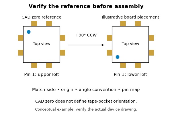
Check the viewing direction before copying a pin position. A component bottom view and PCB top view require the appropriate transformation. Compare the library pin map with the actual device pinout, then verify one polarized or asymmetrical part in the exported placement file. Confirm board side, origin and angle convention with the assembler so the same physical orientation survives the handoff.
Use the assembly drawing to confirm the exported pin-1 position.
Download PDF: IPC-7351B Zero Component Orientation Guide (24 pages)
Which Checks Should a Footprint Pass Before PCB Release?
Approve the part-to-board connection through five checks. Each should leave a specific reviewed output rather than a general statement that the footprint looks correct.
- Component identity: match the BOM and approved alternatives to their package drawings; retain the supported part-number list.
- Library layers: review copper, mask, paste, courtyard and numbering; record the calculation settings and approved exceptions.
- Board placement: run copper and courtyard DRC, then resolve constrained neighbors against the assembly process.
- Manufacturing exports: reopen the fabrication, stencil and placement outputs; confirm units, layers, origin, side and rotation.
- Assembly verification: agree on inspection or test methods for hidden joints and unfamiliar processes, with defined acceptance criteria.
A change to the part, terminal geometry or placement convention reopens the affected checks. Keep the resulting review with the released board revision.
FAQs About IPC-7351 Land Pattern Design
Q1: Can two manufacturer part numbers share one footprint?
A1: Yes, when every approved alternative fits the reviewed geometry. Compare terminal limits, numbering, exposed pads and mounting recommendations. Record the approved part numbers so a purchasing substitution can be distinguished from a new package that still needs engineering review.
Q2: Can a 3D model prove that the copper pads are correct?
A2: No; it supports mechanical checking. A model can expose body collisions or an obvious rotation error, but its terminals may be simplified. Use the controlled drawing and pin map to verify the lands, and check soldering requirements independently of visual alignment.
Q3: Should the courtyard be printed on the silkscreen?
A3: Normally it remains a CAD placement boundary. Silkscreen serves identification and polarity marking on the physical board. Review the legend separately for readability and clearance from exposed pads instead of copying the entire courtyard onto the printed layer.
Q4: Does a courtyard check include component height?
A4: A two-dimensional courtyard does not verify vertical clearance. Compare maximum package height with shields, housings, mating parts and other mechanical constraints. Keep those limits in the mechanical review even when planar placement DRC passes.
Q5: Is pin 1 always the positive terminal?
A5: Pin numbering does not establish polarity. A resistor’s reference pin need not imply an electrical direction, and a diode’s numbered reference may be its cathode. Read the device pinout and marking convention before assigning anode, cathode or positive supply.
Q6: Can thermal vias remain open in a QFN center pad?
A6: That depends on the approved attachment process. Open holes can draw solder away from the joint. Agree on via treatment, stencil design and the required attachment with the assembler; the copper pad outline alone does not specify how the vias are manufactured.
Q7: Can an unused BGA ball be omitted from the footprint?
A7: An electrically unused ball may still be physically present. Distinguish absent positions from populated balls marked NC or reserved. Follow the manufacturer’s land and connection instructions; circuit inactivity alone does not justify removing a copper land or connecting a reserved position.
Q8: Do Gerber files preserve the complete library approval record?
A8: They preserve the exported layer images, not the full design rationale. Retain the BOM, package drawing, calculation settings and approved alternatives with the design release. Placement and assembly data are also needed to communicate the intended component identity and orientation.
Q9: Does IPC-7351 define finished solder-mask and paste-aperture sizes?
A9: Do not treat a copper-land result as a complete mask or stencil specification. A footprint tool may generate those layers, but their settings still need review against the device recommendation, mask process, stencil thickness and required solder deposit before manufacturing release.
Q10: Is there a universal IPC-7351 pad size for 0402 or 0603 components?
A10: No; approve the pattern for the actual component and process. A useful reuse test is to compare the proposed alternative’s terminal limits and mounting recommendation with the library’s supported parts. The shared size code alone is not evidence that the existing pads remain suitable.
Conclusion
IPC-7351 provides a structured route from component geometry and process assumptions to SMT land patterns. Reliable footprints require the inputs and resulting copper arrangement to be checked together, with the applicable standard edition recorded.
For PCB/PCBA manufacturing or a free DFM review of custom footprints, send EBest Circuit the Gerber files, BOM, package drawings and placement data at sales@bestpcbs.com. Include build quantity and any constrained spacing or approved footprint exceptions so the team can review the proposed build and prepare a quotation.
You may also like


Tags: IPC-7351 courtyard, IPC-7351 land pattern calculator, IPC-7351 naming convention, IPC-7351 zero component orientation