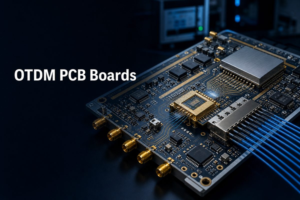
OTDM PCB boards provide the electrical, mechanical, and thermal platform around an optical time-division multiplexing engine. A conventional PCB carries clock, driver, bias, control, and monitor signals; the optical stream is created inside photonic components or optical waveguides, not in ordinary copper traces.
This distinction controls the whole design. The laminate, stackup, RF transitions, power distribution, photonic package, fiber interface, and test plan must be defined as one channel. This guide explains what the board does, where noise enters, and which data a fabricator needs before production.
What Are OTDM PCB Boards?
OTDM PCB boards are circuit boards used around optical time-division multiplexing transmitters, receivers, or laboratory demonstrators. They are not one fixed IPC board class, and the term does not define a universal layer count, material, or connector.
The board may be a high-speed electrical carrier for driver ICs and a photonic package. A more specialized design may be an electro-optical circuit board (EOCB) with embedded glass or polymer waveguides. The correct fabrication route depends on which function is physically inside the PCB.
| Hardware Type | What It Carries | Typical Elements |
| High-speed electrical PCB | Clock, data, bias, power, and control | RF drivers, connectors, power rails, control ICs |
| Electro-optical circuit board | Electrical signals and guided optical paths | Copper layers, embedded waveguides, optical coupling features |
| Photonic module or interposer | Optical modulation, combining, or detection | Modulators, photodiodes, couplers, laser interfaces |
How Does an OTDM Hardware Chain Use the PCB?
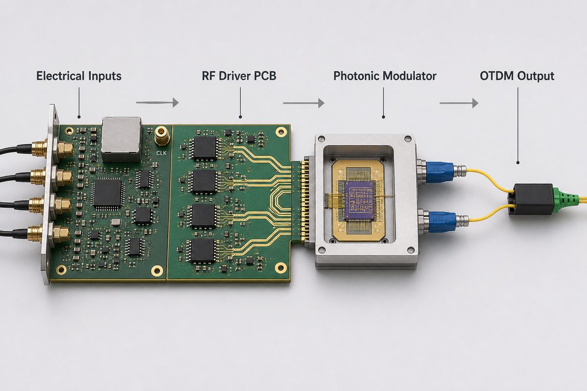
The PCB delivers synchronized electrical channels to a photonic device and supports the power, control, and measurement paths around it. The photonic modulator then interleaves optical pulses in time and passes the combined signal to the fiber interface.
Every boundary can disturb timing. Connector launches, trace length, driver-package transitions, wire bonds, flip-chip interconnects, and bias networks add loss or delay. A strong high-speed PCB design process therefore starts with the complete channel, not a routing rule copied from another board.
Optical Time Division Multiplexing PCB Boards: Electrical PCB or EOCB?
Most optical time division multiplexing PCB boards are best treated as high-speed electrical support boards unless the released design explicitly contains optical waveguides. Copper routes electrical data to a modulator; it does not become an optical path simply because the end system uses OTDM.
True optical time division multiplexing PCBs may combine glass or polymer waveguides with electrical layers. That changes the supplier set, stackup documentation, optical coupling tolerances, material handling, inspection, and qualification plan. The fabrication drawing should state whether the board is electrical-only, an EOCB, or a mechanical carrier for a separate photonic interposer.
Which Stackup and Materials Fit OTDM Support Hardware?
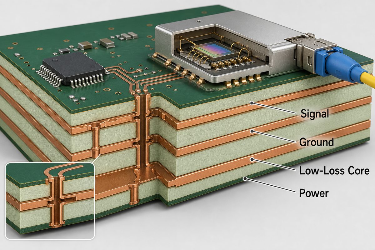
The stackup should preserve the required impedance and loss budget over the actual electrical channel. No single laminate is automatically correct for OTDM; the choice depends on edge rate, trace length, connector loss, package parasitics, thermal load, layer count, and assembly process.
Critical RF layers normally need a nearby continuous reference plane. A stripline can improve field containment, while a microstrip can simplify probing and reduce via transitions. The stripline versus microstrip decision should be made from the channel model and the test-access plan.
- Define the target impedance from the driver, package, and connector interface.
- Use the laminate supplier’s frequency-dependent Dk and Df data for simulation.
- Control dielectric thickness, copper profile, and finished copper when loss margin is tight.
- Keep high-current or noisy power sections away from sensitive RF and photonic interfaces.
- Use HDI only when density or transition length justifies the extra process steps.
How Should RF Routing and Timing Skew Be Controlled?
RF routing should be controlled as one matched path from the electrical source to the photonic load. Length matching alone is insufficient because a longer low-loss trace can perform better than a shorter path with poor launches, stubs, or reference discontinuities.
Route timing-related channels over continuous planes, keep pair geometry stable, and minimize unnecessary layer changes. Model the connector, via field, package landing, and wire-bond or flip-chip transition when those structures consume meaningful channel margin. For dense devices, a multilayer HDI stackup can shorten breakout paths, but it still needs manufacturable anti-pads and reference-via placement.
- Match electrical delay, not only artwork length.
- Keep the return path continuous through every layer transition.
- Avoid open stubs and test pads on the highest-speed paths unless modeled.
- Place ground vias near RF transitions and connector launches.
- Release the impedance model and tolerance with the fabrication data.
OTDM PCB Boards Noise Control
OTDM PCB boards noise control depends on separating low-noise photonic bias and clock paths from switching power, digital control, and connector return currents. Noise that shifts a modulator’s operating point or adds clock jitter can reduce the usable timing margin even when trace impedance is correct.
Poor OTDM PCB boards noise performance often starts with a shared return path, a noisy regulator, excessive power-loop inductance, or coupling between parallel channels. Partition the power distribution by function, place decoupling at the load, and keep sensitive bias loops compact. Do not place a plane split under a fast signal to create artificial isolation; the broken return path can increase radiation and common-mode conversion.
How Should Photonic Devices Be Packaged on the Board?
Photonic packaging should minimize electrical parasitics while keeping optical alignment mechanically stable. The board cannot be designed independently from the modulator, photodiode, fiber array, interposer, wire-bond geometry, connector, and heat-removal method.
Short RF interconnects are usually preferred, but the shortest geometry is not always the most manufacturable or inspectable. Agree on pad finish, bondable surface, cavity or cutout dimensions, component keep-outs, fiber bend radius, connector retention, lid clearance, and rework access before the PCB is released. If optical waveguides are embedded, add the coupling datum and optical test structure to the controlled drawing.
Which Thermal and Mechanical Risks Need Attention?
Thermal expansion, board warpage, connector force, and local heating can shift electrical or optical alignment. A board that passes a room-temperature bench test may still fail after assembly stress or temperature cycling if the package, PCB, and fiber fixture move differently.
- Check heat flow from drivers, regulators, lasers, and the photonic package.
- Keep mounting-hole and stiffener loads away from optical alignment features.
- Control copper balance and stackup symmetry where flatness is critical.
- Define the allowable reflow profile for every optical and electronic component.
- Protect fiber exits from sharp bending, strain, and assembly-tool access.
Use simulation as a design aid, then confirm the assembled structure with measurements. Material properties, package construction, enclosure airflow, and fixture stiffness must come from the actual project rather than a generic OTDM reference design.
How Should OTDM PCB Boards Be Tested?
Testing should separate bare-board quality, assembled electrical-channel performance, and optical-system performance. A bare PCB can pass continuity and impedance checks while the assembled OTDM channel still fails because of a connector, package transition, bias condition, or optical alignment issue.
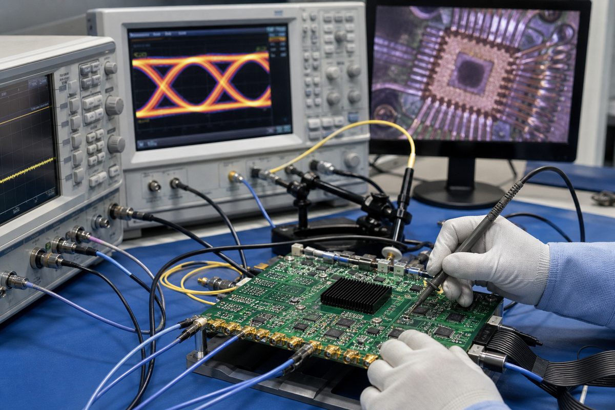
Bare-board checks may include electrical testing, impedance coupons, dimensional inspection, microsection review, and copper-thickness verification. Assembly inspection can use AOI and X-ray where applicable. Channel validation may add TDR, VNA measurements, clock and jitter checks, and an eye diagram under the intended operating pattern.
| Test Stage | Core Check | Typical Evidence |
| Bare PCB | Connectivity, impedance, dimensions, and build quality | E-test record, coupon result, inspection report |
| PCB assembly | Joints, package placement, power rails, and interfaces | AOI, X-ray where applicable, functional checks |
| Electrical channel | Loss, reflection, skew, and jitter contribution | TDR, VNA, oscilloscope, eye diagram |
| Optical system | Pulse timing, combining, detection, and system margin | Project-specific optical test plan |
What DFM Data Should Be Released to Fabrication and Assembly?
The release package should define the electrical channel, physical stackup, photonic interface, and acceptance evidence. Gerber files alone cannot communicate the assumptions behind a low-loss, timing-sensitive optoelectronic board.
- Gerber or ODB++ data, drill files, profile, and fabrication drawing
- Approved stackup with laminate family, copper, and dielectric requirements
- Single-ended and differential impedance targets with coupon requirements
- RF connector, photonic package, fiber-interface, and mechanical drawings
- Critical-net list, length or delay constraints, and reference-layer information
- BOM, assembly drawing, pick-and-place data, and reflow restrictions
- Bare-board, assembly, electrical-channel, and optical-system test responsibilities
Any embedded waveguide, optical via, cavity, bondable finish, or alignment datum should be called out explicitly. It must not be left for the fabricator to infer from copper artwork.
FAQ About OTDM PCB Boards
- Does an OTDM PCB carry optical data through copper traces? No. A conventional PCB carries the electrical drive, clock, bias, control, and monitor signals. Optical multiplexing occurs in a photonic device or optical waveguide structure.
- Is every OTDM board an optical PCB? No. Many OTDM demonstrators and modules use an electrical PCB connected to a separate photonic chip. An optical PCB or EOCB integrates waveguides into the board structure.
- Does an OTDM support board always need low-loss laminate? Not always. Material choice depends on electrical edge rate, trace length, loss budget, connector and package transitions, thermal needs, and cost. The channel model should drive the decision.
- Can FR-4 be used for an OTDM support PCB? It may be suitable for short electrical paths or lower-loss demands, but the exact laminate must be checked against frequency-dependent loss, impedance, thermal, and assembly requirements.
- Which files are needed for an OTDM PCB quotation? Send fabrication data, stackup, impedance requirements, critical-net constraints, mechanical and photonic interface drawings, BOM, assembly files, quantity, and test requirements.
How Can EBest Circuit Support Your OTDM Hardware Project?
At EBest Circuit, we support the high-speed electrical PCB and PCBA portion of optoelectronic hardware through stackup review, controlled-impedance fabrication, HDI options, component sourcing, assembly, electrical testing, AOI, X-ray inspection where applicable, and engineering review. If the design includes embedded optical waveguides or another nonstandard optical layer, we will first separate that scope from the conventional PCB work and review the manufacturing path with you.
Send your Gerber files, stackup, BOM, impedance targets, photonic package drawing, quantity, and test requirements to sales@bestpcbs.com. We can review the board construction and identify the electrical, assembly, and interface details that should be settled before quotation.
For a stable release, keep the final OTDM PCB boards specification tied to the actual photonic module, RF channel, and verification plan.