In the design of electronic products, electromagnetic compatibility (EMC) is a crucial consideration. Particularly in the design of printed circuit boards (PCBs), the rationality of EMC design directly impacts the performance and stability of the product. Among the many factors affecting EMC, one factor is especially critical, and that is the design of the ground plane. Today, let’s talk about the impact of grounding on EMC.
In an electronic product, grounding is a very important element, it is directly related to EMC compliance. Especially in large equipment, the grounding of multiple systems and subsystems is involved. It can be said, a good grounding system means the half successfully of a product.

What are Ground Plane and EMC in a PCB?
The ground plane, as the reference potential in a circuit, not only carries the return path of current but also plays a role in electromagnetic shielding and noise suppression. In high-frequency circuits, the impedance and layout of the ground plane have a significant impact on signal integrity. Unreasonable ground plane design may result in signal interference, increased radiation, and decreased system stability.
EMC stands for Electromagnetic Compatibility. It refers to the ability of electronic devices and systems to operate properly in their intended electromagnetic environment without causing or experiencing interference. EMC ensures that devices can function without adversely affecting other devices nearby or being affected by electromagnetic interference from external sources. Generally, the ground planes will showing three shapes, please see as following:

Why A Grounding Must be Designed in PCB?
Grounding can be understood as an equipotential point or plane serving as the reference potential for a circuit or system, which can be a specific ground layer in a PCB or the metal chassis of a product. While many perceive the purpose of designing a ground plane primarily to prevent external electromagnetic interference (EMI), but in printed circuit board design, it serves multiple purposes beyond this.
Generally, a well-designed ground provides a common reference zero potential for all circuit units within a system, ensuring no potential difference between circuits and thus stable operation. It also protects circuits from damage, ensuring the safe functioning of electronic products. For instance, ground can provide discharge paths for transient disturbances and dissipate accumulated charges on product metal enclosures induced by static electricity, to prevent potential sparks that may cause interference internally. Additionally, choosing appropriate grounding for shielding structures can yield effective electromagnetic shielding.
Grounding design is very necessary especially for medical industry. As we know, there are many medical devices are directly connected to patients’ bodies, such as monitors. In cases where the chassis carries voltage due to poor grounding, fatal risks may arise. Furthermore, grounding reduces common-mode interference currents flowing through PCBs and prevents high-frequency EMI signals within products from reaching equivalent radiating antennas. Thus, grounding is typically a primary method for noise suppression and interference prevention.
Design Principles of Ground Plane in PCB
A well-designed grounding system should not only consider the radiation and conduction of individual PCBs but also prevent from a systemic perspective. In the design phase, failure to carefully consider the grounding system may indicate a high likelihood of EMC failure for the system. So, knowing the design principles is extremely important to make sure the successful of EMC.
- Keep it short and wide
To reduce the impedance of circuits, especially in high-frequency circuits, the ground plane should be made as short and wide as possible. This helps to minimize the return path of the current, thereby reducing EMI.
- Partition layout
For complex PCB designs like multilayer PCBs, it is recommended to use a partition layout to separate the ground planes of different functional modules. This helps to isolate noise interference between different modules.
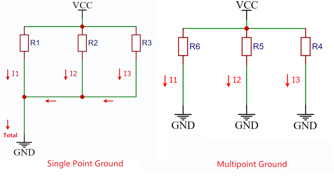
- Single-point ground and multipoint ground
Depending on the circuit’s operating frequency and signal characteristics, choose between single-point grounding or multipoint grounding. Single-point grounding is suitable for low-frequency circuits, while multipoint grounding is more suitable for high-frequency circuits.
- Ground plane
Where possible, use a ground plane as the ground. The ground plane can provide a low-impedance return path and aid in electromagnetic shielding.
How to Optimize Your Grounding Design?
As for PCB that has already design the circuit layout, how to optimize the ground to get the maximum EMI? Here are some tips that may helpful for you.
- Fill the blank areas of the PCB with ground planes to increase the ground plane’s area and reduce impedance.
- Reducing the area of ground loops helps to decrease electromagnetic radiation and induced noise.
- Power lines and ground planes should be placed as close as possible and run parallel to reduce the area of the current loop.
- Placing decoupling capacitors between power and ground planes helps to filter out high-frequency noise.
In PCB EMC design, ground plane design is an essential step that cannot be ignored. By following the principles and optimization methods of ground plane design, the EMC and signal integrity of electronic products can be significantly improved. Therefore, in PCB design, sufficient attention and consideration must be given to ground plane design. Welcome to contact EBest Circuit (Best Technology) if you want to know more about ground and EMC design.
You may also like


Tags: EMC, GND design, pcb design, pcb EMC