PCB manufacturing PCB manufacturing
Home > Blog

hdi pcb design guidelines

UHDI Printed Circuit Board: Design Rules, Stackup, and DFM
Tuesday, September 1st, 2026

A UHDI printed circuit board moves beyond conventional HDI when at least one critical feature enters the ultra-fine range. That change affects far more than trace width. The imaging method, copper build, microvia geometry, dielectric thickness, registration plan, solder mask, inspection criteria, and assembly interface must be treated as one manufacturing system.

This guide helps design and procurement teams decide whether a project is truly UHDI, where early DFM work prevents redesign, and what evidence should be agreed before prototype release. It also separates published working thresholds from a supplier’s confirmed production capability—an important distinction when yield, reliability, and repeatability matter.
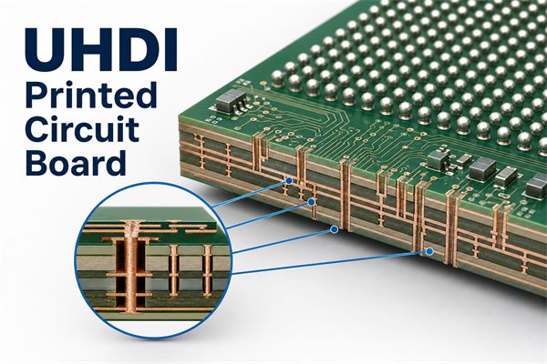
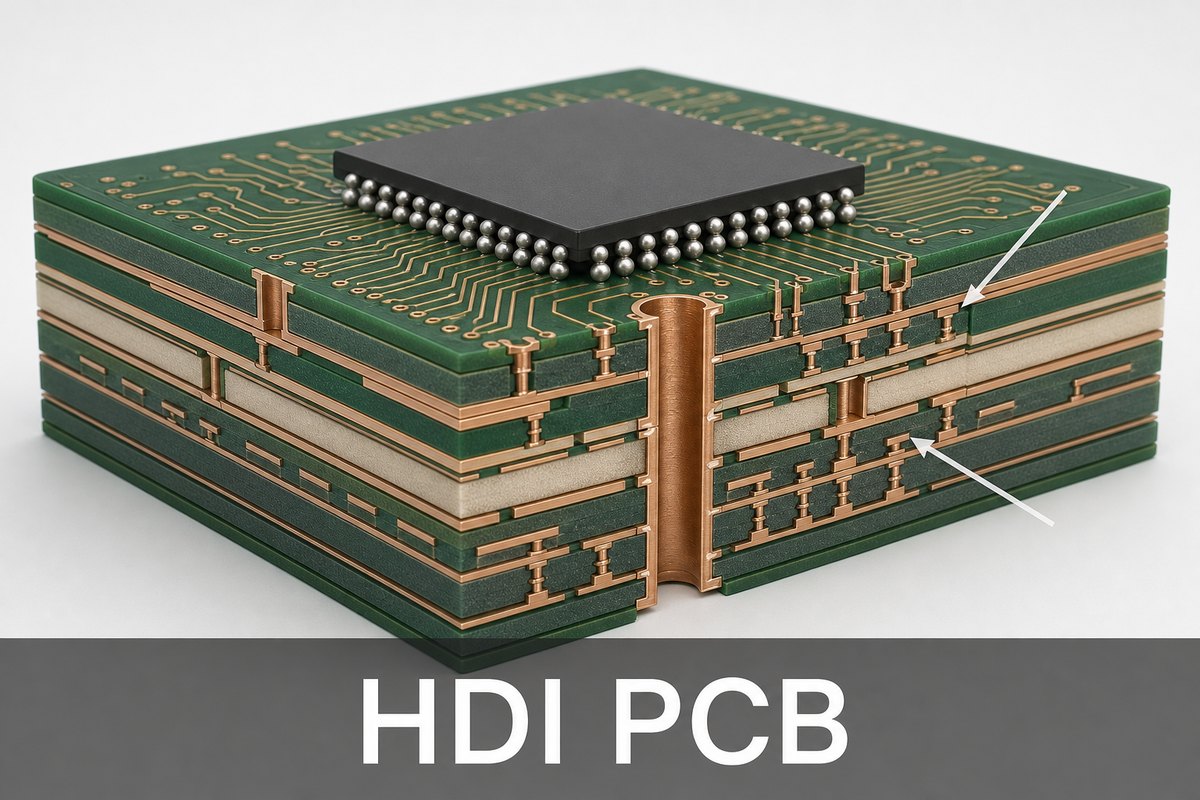
UHDI printed circuit board with ultra-fine traces and laser microvias

What Is a UHDI Printed Circuit Board?

UHDI means ultra-high-density interconnect. The industry’s working definition generally places a board in UHDI territory when one or more features go beyond the highest conventional HDI producibility range. Common reference thresholds include:

  • Conductor line width below 50 µm.
  • Conductor spacing below 50 µm.
  • Build-up dielectric thickness below 50 µm.
  • Laser microvia diameter below 75 µm.

These figures are useful screening points, not permission to combine every minimum on one design. A board with 45 µm spacing on one layer may require a different process route from a board with 60 µm traces and 50 µm microvias. Material, copper thickness, panel format, feature distribution, registration tolerance, surface finish, and annual volume all affect the real production window.

The shorter phrase ultra hdi pcb often refers to the same technology. In practice, the fabrication drawing should state the actual features and acceptance requirements instead of relying on the label alone.

How Does UHDI Differ from Conventional HDI?

Conventional HDI gains density through laser microvias, blind or buried connections, sequential lamination, and via-in-pad. UHDI keeps those concepts but pushes selected geometries beyond conventional HDI process limits. That shift changes both the fabrication method and the amount of process verification required.

Design Area Conventional HDI UHDI Consideration
Fine conductors Often produced by optimized subtractive etching May require mSAP, SAP, or another ultra-fine-line process
Microvias Laser-drilled vias commonly around the 0.10 mm class Smaller geometry needs tighter drilling, plating, and registration control
Dielectrics Build-up films selected around a proven HDI stackup Very thin dielectrics make copper balance and via aspect ratio more sensitive
Inspection AOI, electrical test, impedance test, and microsection as specified More detailed coupons, dimensional evidence, and agreed acceptance rules may be needed

A designer should therefore ask, “Which features require UHDI?” rather than applying ultra-fine geometry across every layer. Restricting the most demanding rules to the package escape or other density-critical zones can improve yield and cost without sacrificing electrical performance.

HDI PCB Design Guidelines for UHDI Layouts

Useful hdi pcb design guidelines begin with the fabricator’s production window, not the CAD tool’s minimum setting. The following decisions should be closed before routing is frozen:

  • Define the density driver. Record BGA pitch, pad diameter, escape count, available routing channels, and the layers that genuinely need ultra-fine features.
  • Use regional rules. Keep wider traces and spaces outside dense package fields where possible. A mixed-rule design is usually easier to control than a board built entirely at the minimum.
  • Separate line and space values. Do not assume a supplier’s minimum line width automatically permits the same minimum clearance after plating.
  • Coordinate copper with geometry. Thicker copper is harder to resolve into very fine conductors. Base copper and final copper must both appear in the fabrication notes.
  • Treat solder mask as a precision layer. Mask registration, dam width, pad definition, and via treatment can determine whether fine-pitch assembly is practical.
  • Control impedance from the real stackup. Trace geometry, dielectric thickness, resin content, copper profile, and reference-plane distance must be reviewed together.

Do not design every feature at a supplier’s stated limit. The published minimum may describe a test coupon or a restricted build, while the stable production value may be wider. A useful DFM conversation distinguishes prototype feasibility, repeatable production, and the conditions attached to each.
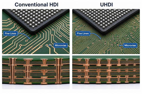
Comparison of conventional HDI and UHDI PCB trace and microvia geometry

HDI PCB Stackup Decisions for UHDI

An hdi pcb stackup cannot be finalized independently from the escape strategy. The number of build-up layers, microvia spans, plane assignment, material family, and impedance targets determine the lamination sequence and the inspection plan.

Review these points together:

  • Build-up architecture: confirm whether 1+N+1, 2+N+2, any-layer, or another construction is actually required.
  • Microvia type: use staggered microvias where routing permits; specify stacked structures only where density justifies the additional process and reliability burden.
  • Via aspect ratio: match microvia diameter to dielectric depth. A small opening through an unnecessarily deep dielectric creates plating risk.
  • Via fill and cap: via-in-pad normally requires a defined fill, planarization, and cap-plating sequence before component assembly.
  • Stack symmetry: balance copper and dielectric construction to reduce bow, twist, and registration drift through repeated thermal cycles.
  • Material availability: confirm the exact laminate, build-up film, copper foil profile, thickness tolerance, and approved substitutes before impedance values are released.

Early stackup review is especially important when UHDI routing is combined with high-speed interfaces. Our existing guide to HDI PCB structures explains conventional 1+N+1, 2+N+2, and every-layer interconnect concepts, while the separate 80 GHz UHDI PCB article focuses on RF material and impedance concerns.
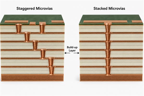
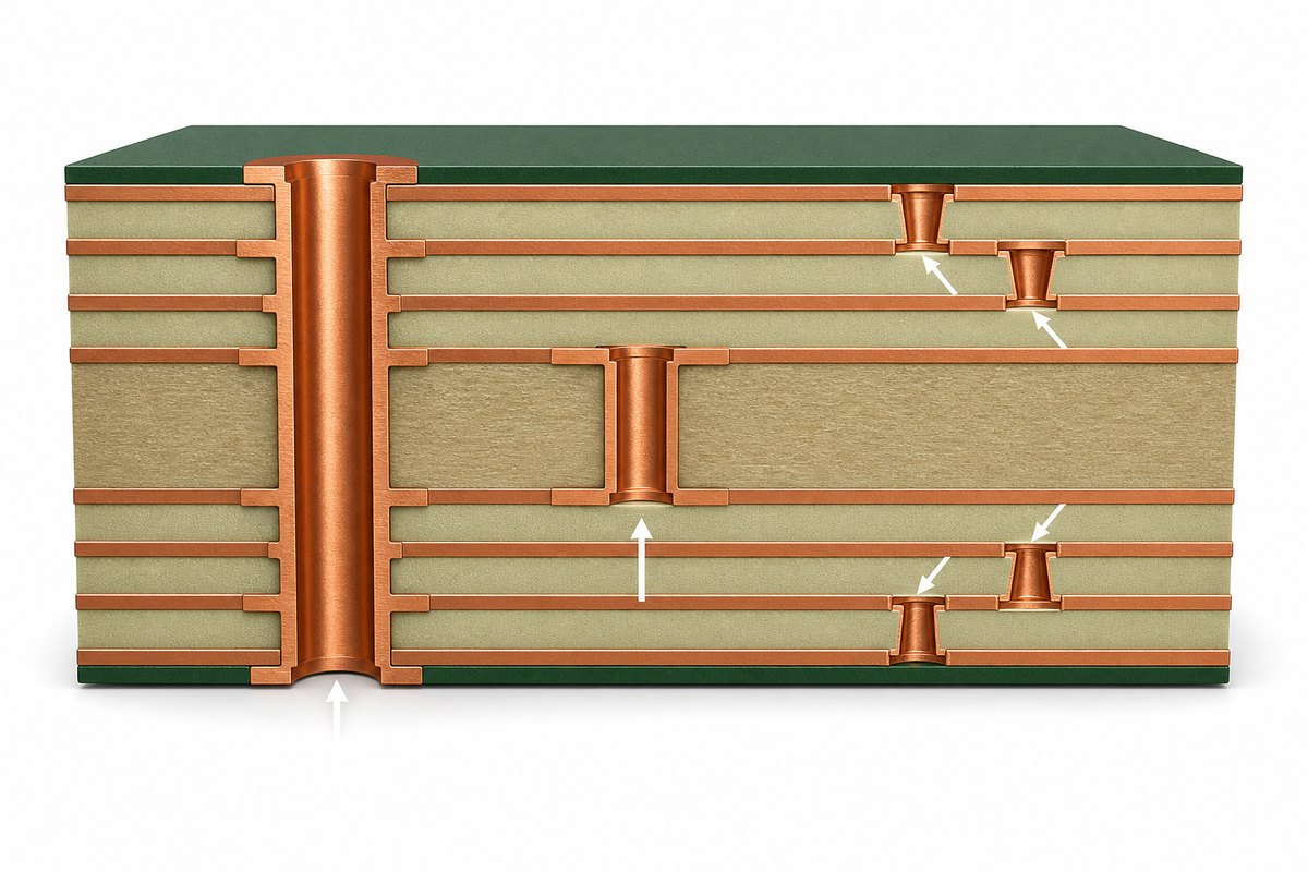
UHDI PCB stackup showing staggered and stacked laser microvias

How Does the HDI PCB Manufacturing Process Change for UHDI?

The hdi pcb manufacturing process normally uses sequential build-up, laser drilling, copper deposition, imaging, plating, lamination, and electrical verification. UHDI adds tighter interactions between these steps and may change the conductor-forming method.

  1. Engineering review: identify every sub-50 µm feature, microvia span, impedance structure, copper requirement, and inspection coupon.
  2. Material and process selection: choose a laminate, build-up dielectric, copper foil, and imaging route that can hold the requested geometry.
  3. Core and build-up imaging: form fine conductors with a process selected for the target line, space, and copper thickness.
  4. Laser drilling and desmear: control via diameter, taper, landing accuracy, and the condition of the target pad.
  5. Metallization and filling: establish reliable copper in the microvia, fill specified structures, and planarize via-in-pad surfaces.
  6. Sequential lamination: repeat build-up cycles while controlling registration, resin flow, copper balance, and thickness.
  7. Surface formation: apply solder mask and surface finish without consuming the clearances needed for fine-pitch assembly.
  8. Inspection and test: use AOI, electrical testing, microsection, dimensional measurement, impedance testing, or other project-specific evidence.

Subtractive etching can support some near-UHDI geometries, but very fine and consistent conductors may require modified semi-additive or semi-additive processing. The correct route depends on feature size, copper thickness, layer location, panel scale, volume, and supplier capability. It should be confirmed before the layout is locked.

Which DFM Risks Cause UHDI Prototype Failure?

UHDI prototypes most often become expensive when a local density decision triggers an unplanned process change. The risk is rarely one number in isolation.

  • Minimum geometry used everywhere: reduces the process margin across the whole panel even though only a small BGA area needs it.
  • Excessive stacked microvias: increases lamination count and concentrates thermo-mechanical stress.
  • Unconfirmed copper build: fine lines may not survive the plating and etching sequence at the requested final copper.
  • Ambiguous via notes: missing fill, cap, target-layer, or aspect-ratio requirements can change both cost and reliability.
  • Late impedance modeling: forces trace-width or dielectric changes after routing is complete.
  • Insufficient mask clearance: causes assembly constraints even when the copper pattern can be fabricated.
  • No agreed acceptance plan: leaves the customer and supplier evaluating fine features with different criteria.

A strong DFM response should show what must change, why it matters, and whether the recommendation affects electrical performance. “Cannot build” is not enough; the customer needs an alternative feature, stackup, or process route.

What Inspection Evidence Should Be Defined?

Electrical continuity alone cannot prove that a UHDI process is stable. The inspection plan should follow the critical risks in the design and may include:

  • AOI coverage for fine-line layers.
  • Microsection locations that represent stacked or staggered microvias.
  • Measurement of finished line width, spacing, dielectric thickness, and via geometry.
  • Impedance coupons that match the controlled layers and copper construction.
  • Electrical test coverage and netlist source.
  • Surface-finish thickness or wire-bond acceptance criteria when applicable.
  • Assembly X-ray or other inspection for fine-pitch packages when the project includes PCBA.

At EBest Circuit, our documented quality resources include AOI, electrical testing, impedance testing, microsection inspection, copper-thickness testing, 2D measurement, and X-ray inspection for relevant assembly work. The final test plan still depends on the product, customer specification, and confirmed process route. See our PCB quality and testing overview for the broader control framework.
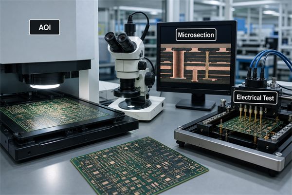
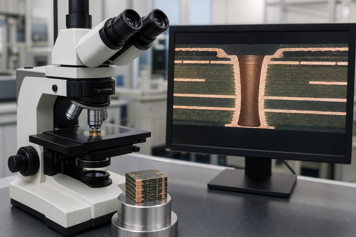
UHDI PCB microsection and automated optical inspection workflow

How Do UHDI Choices Affect Cost and Lead Time?

UHDI does not automatically make the lowest system cost, even when it reduces board area. Cost and lead time rise when a design adds specialized material, semi-additive conductor formation, more lamination cycles, stacked microvias, tight registration, extra coupons, or low-yield feature combinations.

The practical cost levers are:

  • How many layers actually need ultra-fine line and space.
  • Whether a standard panel and material construction can be used.
  • The number of sequential lamination cycles.
  • Staggered versus stacked microvia architecture.
  • Base and finished copper thickness.
  • Surface finish and fine-pitch assembly requirements.
  • Prototype quantity, test evidence, and volume forecast.

A compact UHDI board can still lower total product cost when it removes connectors, reduces board area or layer count, shortens critical interconnects, or enables a smaller enclosure. The comparison should therefore use total system impact, not PCB unit price alone.

What Should Be Included in a UHDI RFQ Package?

Provide enough information for the supplier to evaluate the exact feature combination. A useful package includes:

  • Gerber or ODB++ fabrication data and the fabrication drawing.
  • Proposed layer stackup, material family, finished thickness, and copper weights.
  • A list of the minimum line, minimum spacing, smallest microvia, and affected layers.
  • Microvia spans, stacked or staggered structure, via fill, and cap-plating notes.
  • Controlled-impedance table and reference-layer information.
  • Surface finish, solder mask, legend, and assembly constraints.
  • Test standard, inspection evidence, coupon requirements, and acceptance class.
  • Prototype quantity, expected annual volume, and requested delivery date.
  • BOM, pick-and-place data, and assembly drawing when PCBA is required.

For a general supplier overview, you can also review our existing UHDI PCB fabrication page. Its purpose is supplier selection, while this page is intended to help engineering teams prepare a manufacturable design package.

FAQ About UHDI Printed Circuit Boards

Is every board with microvias a UHDI PCB?

No. Microvias are common in conventional HDI. UHDI is associated with one or more features beyond conventional HDI thresholds, such as sub-50 µm lines or spaces, sub-50 µm build-up dielectrics, or microvias below the 75 µm range.

Does UHDI always require mSAP?

No. The conductor-forming method depends on the target geometry, copper thickness, layer, panel, and supplier. Some near-UHDI features may be possible with advanced subtractive control, while tighter and more uniform conductors may need mSAP or SAP.

Are stacked microvias better than staggered microvias?

Not automatically. Stacked microvias save routing area, but they add process complexity and reliability sensitivity. Use them where density requires them; use staggered structures where the layout allows a more forgiving construction.

Can standard HDI design rules be reused for UHDI?

They are a starting point, not a release condition. UHDI requires a supplier-specific review of fine-line formation, dielectric depth, via geometry, copper build, registration, solder mask, inspection, and production volume.

How Can EBest Circuit Review Your UHDI Project?

EBest Circuit has provided PCB and PCBA support since 2006. We work with customers on PCB design review, prototyping, multilayer and HDI fabrication, component sourcing, assembly, and testing. Our documented management and compliance resources include ISO 9001:2015, ISO 13485:2016, IATF 16949, AS9100D, UL, RoHS, and REACH; applicability should be confirmed for the specific product and production route.

For a true UHDI request, we do not treat a marketing label as a capability approval. Our team first reviews the line and space by layer, dielectric construction, microvia geometry, copper build, stackup, impedance, surface finish, quantity, and required evidence. We then confirm whether the project fits an available process route or needs design adjustment. You can also review our broader PCB manufacturing capability information.

Send your Gerber or ODB++ files, stackup, impedance table, fabrication drawing, quantity, and test requirements to sales@bestpcbs.com. We will help identify the density-critical features, return practical DFM feedback, and confirm a manufacturable path for your UHDI printed circuit board before quotation.


You may also like

14-Layer HDI PCB: Stackup, Design Rules & Manufacturing Guide
Wednesday, August 19th, 2026

A 14 layer HDI PCB combines 14 copper layers with high-density interconnect features such as microvias, blind and buried vias, sequential lamination, and via-in-pad.

The extra layers provide room for signals, ground planes, and power distribution. HDI technology solves the routing problem around fine-pitch components, where conventional through vias consume too much board space.

Before selecting this structure, engineers usually need to determine:

  • How many HDI buildup layers are necessary?
  • Can the BGA be routed without stacked microvias?
  • Which stackup supports the required impedance?
  • Can the laminate tolerate repeated lamination?
  • Which fabrication limits should be confirmed before layout is frozen?

These choices have a larger impact on cost and manufacturability than the layer count alone.

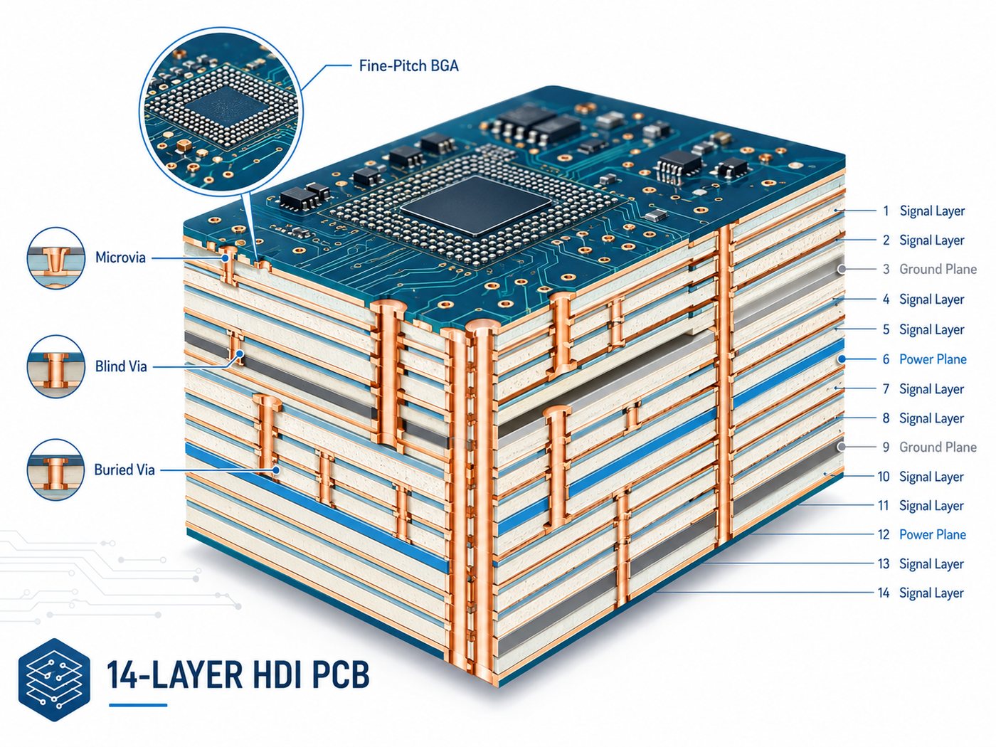
14-layer HDI PCB cutaway showing microvias, blind vias, buried vias, signal layers, ground planes and power planes

What Is a 14-Layer HDI PCB?

A 14-layer HDI PCB has 14 conductive copper layers and uses high-density vias to connect selected layers.

Common HDI features include:

  • Laser-drilled microvias
  • Blind and buried vias
  • Via-in-pad
  • Stacked or staggered microvias
  • Sequential buildup layers

A conventional 14 layer PCB can also have 14 copper layers but rely mainly on through vias.

HDI becomes useful when a design needs more routing channels around fine-pitch BGAs, processors, FPGAs, or other dense packages. If component pitch is generous and board area is not constrained, a conventional multilayer board may be the more economical choice.

When Do You Need a 14-Layer HDI PCB?

A 14-layer HDI construction makes sense when routing density, board size, and electrical requirements begin competing for the same space.

Typical cases include:

  • Fine-pitch BGA breakout
  • High-I/O processors or FPGAs
  • Compact communication or computing boards
  • Multiple high-speed interfaces
  • Designs requiring several continuous reference planes
  • Dense layouts where through vias block inner-layer routing

HDI should solve a specific layout problem. If a standard 14-layer board can meet routing and electrical requirements without microvias or sequential buildup, adding HDI only increases fabrication complexity.

How Is a 14-Layer HDI PCB Stackup Designed?

A 14 layer PCB stackup should be built around routing, impedance, power distribution, board thickness, and via structure.

The HDI PCB stackup must be reviewed with the approved laminate system, finished thickness, copper distribution, and impedance targets before routing is released.

For a broader explanation of layer planning, see our PCB board stackup guide.

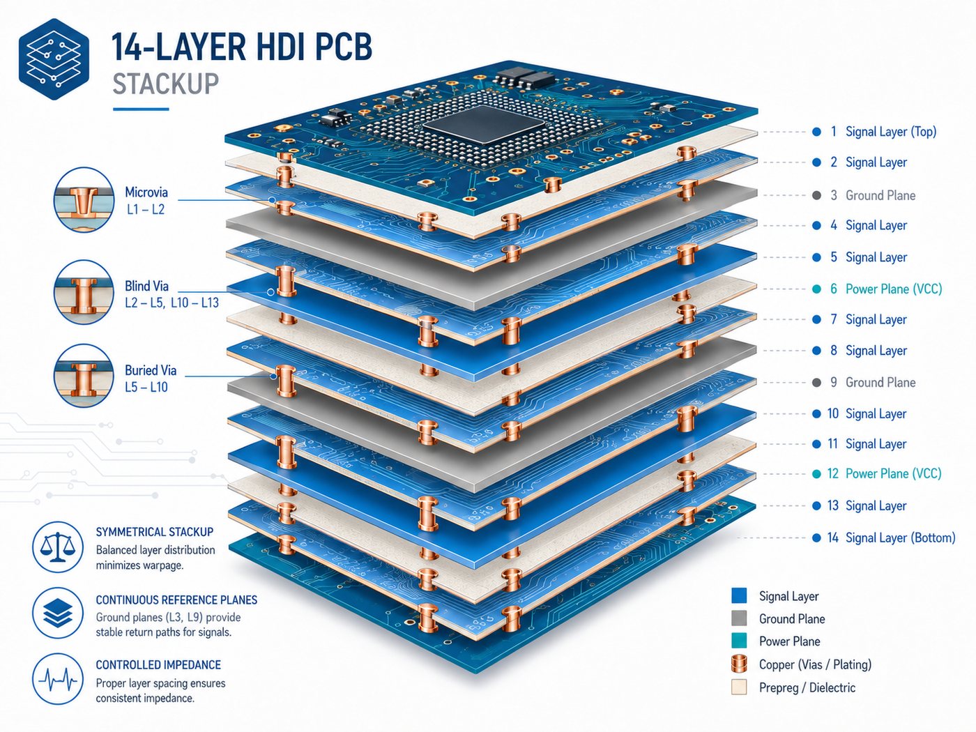
Exploded 14-layer HDI PCB stackup showing signal layers, ground planes, power planes, microvias and blind vias

One possible arrangement is:

Layer Typical Function
L1 Components / high-speed signal
L2 Ground
L3 High-speed signal
L4 Ground
L5 Signal
L6 Power
L7 Ground
L8 Ground
L9 Power
L10 Signal
L11 Ground
L12 High-speed signal
L13 Ground
L14 Components / signal

This is an example, not a universal stackup. Actual dielectric thickness, copper weight, and layer assignment depend on the design.

Three practical rules are useful:

  • Keep high-speed signal layers next to continuous reference planes.
  • Maintain a reasonably symmetrical construction to reduce warpage risk.
  • Define the HDI layer stackup together with the microvia structure.

For example, if microvias connect L1-L2 and L2-L3, the dielectric thickness between those layers must suit the selected laser-via geometry. Stackup review should therefore happen before final routing.

Which HDI Buildup Structure Should a 14-Layer PCB Use?

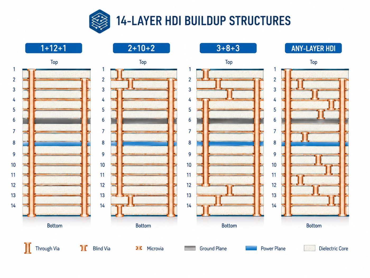
The buildup defines how many HDI layers are added around the central multilayer structure.

Comparison of 1+12+1, 2+10+2, 3+8+3 and any-layer HDI buildup structures for a 14-layer PCB
Structure Typical Use
1+12+1 Moderate-density outer-layer breakout
2+10+2 Higher-density BGA routing
3+8+3 Very dense component areas
Any-layer HDI Designs requiring maximum interconnection flexibility

A 1+12+1 structure is suitable when signals mainly need to move from the outer layer into the first internal routing layer.

A 2+10+2 structure provides more routing freedom around dense BGAs or processors.

Moving to 3-step or any-layer HDI should have a clear routing benefit. More buildup stages mean additional lamination, laser drilling, plating, filling, and registration control. The best structure is usually the simplest one that completes the routing without compromising electrical requirements.

How Should Microvias, Blind Vias, and Buried Vias Be Used?

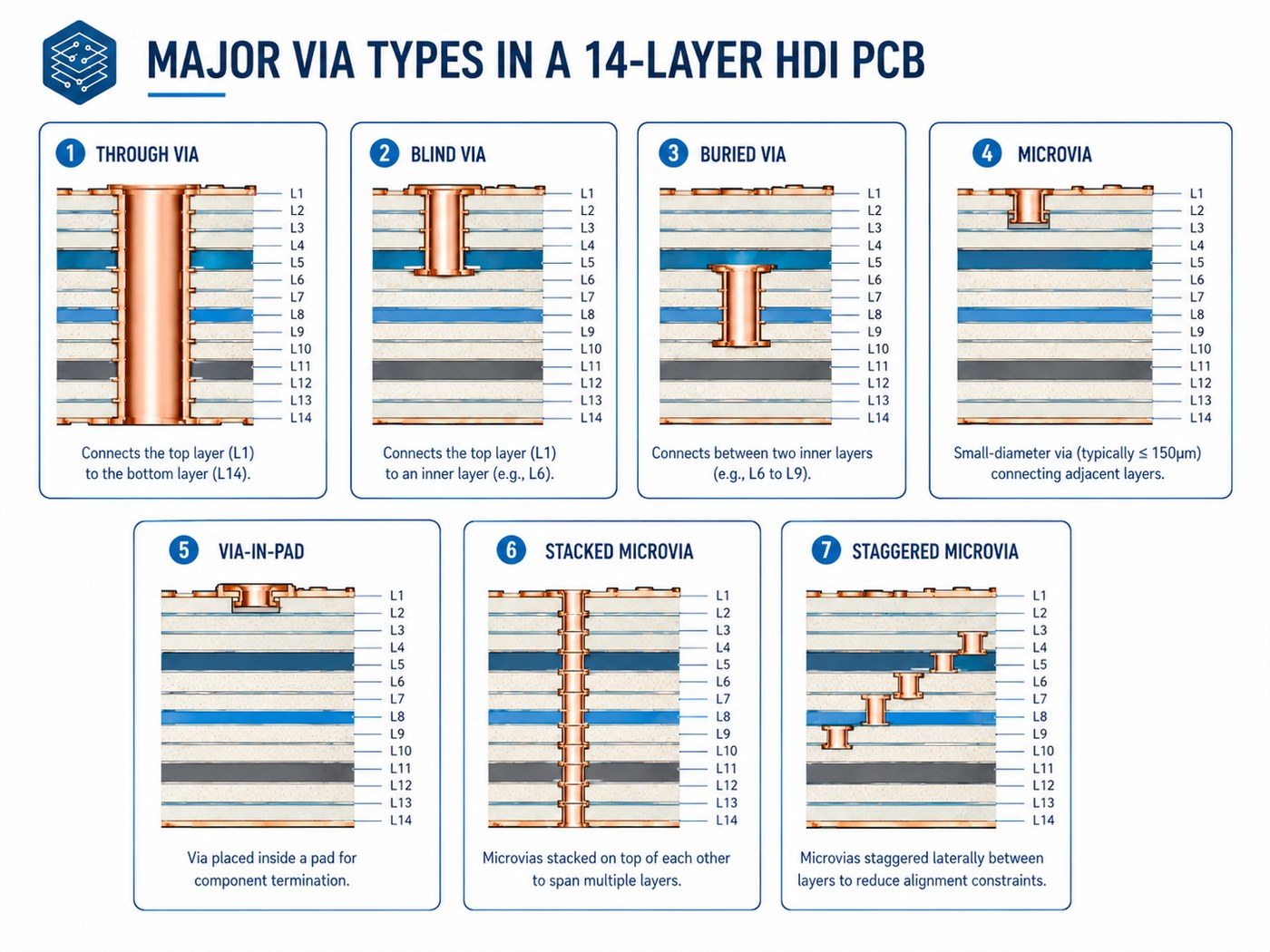
Each via type has a different job.

Through via, blind via, buried via, microvia, via-in-pad, stacked microvia and staggered microvia comparison
Via Type Best Use
Through via General connections in lower-density areas
Blind via Outer-to-inner layer connections
Buried via Internal layer-to-layer routing
Microvia Fine-pitch routing between nearby layers
Via-in-pad BGA and small-package breakout
Stacked microvia Maximum routing density
Staggered microvia Multi-level routing where offset space is available

Stacked microvias save space but require tighter control of:

  • Copper filling
  • Layer registration
  • Plating quality
  • Thermal reliability

Staggered microvias are often easier to manufacture when the layout has enough space for an offset transition.

Via-in-pad is useful under fine-pitch BGAs. These vias normally need to be filled and planarized so the component pad remains flat and solderable.

What Are the Key 14-Layer HDI PCB Design Rules?

These HDI PCB design guidelines should match the manufacturer’s actual production capability rather than a generic CAD rule set.

Confirm these items before layout is finalized:

  • Microvia diameter and depth
  • Capture-pad size
  • Annular ring
  • Minimum trace and space
  • Via-to-pad clearance
  • Via filling requirements
  • Stacked microvia capability
  • Layer registration tolerance
  • Controlled impedance

Avoid using the factory’s absolute minimum geometry across the entire board. A feature that can be produced in a small isolated area may not be the best choice for stable volume production.

Copper balance should also be considered across the stack. Large differences in copper distribution between corresponding layers can increase warpage risk.

For controlled impedance, provide the target values and net types. Trace dimensions can then be adjusted against the actual laminate and finished dielectric thickness.

How Do You Control Signal and Power Integrity in a 14-Layer HDI PCB?

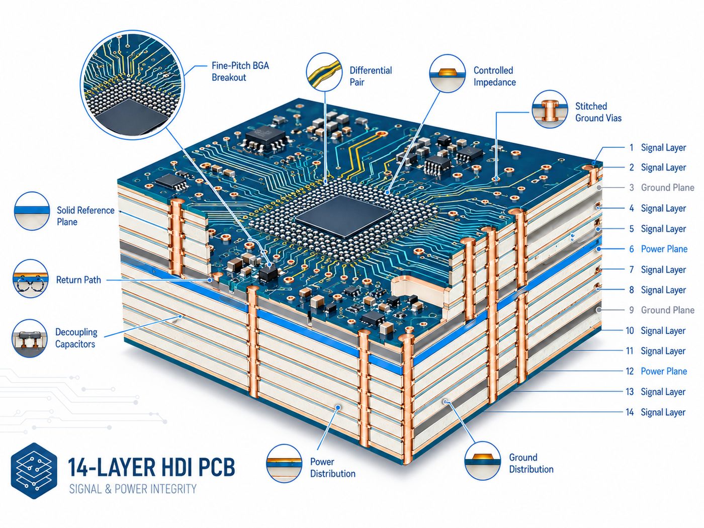
Fourteen layers provide useful flexibility for signal and power planning, but only if the reference structure is well organized.

14-layer HDI PCB signal and power integrity illustration with fine-pitch BGA breakout, differential pairs, reference planes and stitching vias

For signal integrity:

  • Route high-speed traces next to solid reference planes.
  • Avoid routing across plane splits.
  • Keep differential-pair geometry consistent.
  • Add nearby ground vias when signals change reference layers.
  • Use short microvia transitions where appropriate.
  • Avoid unnecessary through-via stubs.

For power integrity:

  • Provide low-inductance paths between power and ground.
  • Keep critical power planes close to their return planes where practical.
  • Place decoupling close to high-current and fast-switching devices.
  • Avoid fragmented return paths around plane cutouts.

The benefit of a 14-layer structure is not simply “more layers.” It is the ability to separate routing, reference, and power functions without forcing too many compromises.

Which Materials Are Suitable for a 14-Layer HDI PCB?

Material choice depends on electrical loss, thermal stress, and repeated-lamination requirements.

Material Type Typical Fit
High-Tg FR-4 General industrial HDI
Low-loss FR-4 Higher-speed digital designs
High-performance laminate Demanding thermal or reliability requirements
Hybrid stackup Designs where only selected layers need special properties

Important parameters include:

  • Tg
  • Z-axis CTE
  • Dk
  • Df
  • Resin system
  • Moisture behavior
  • Repeated-lamination performance

For high-speed designs, Dk and Df affect impedance and transmission loss. For multilayer HDI, Z-axis expansion and laminate stability also matter because vias experience repeated thermal stress during fabrication and assembly.

Material availability should be checked before quotation. An uncommon laminate can add unnecessary sourcing time even when the PCB design itself is straightforward.
How Is a 14-Layer HDI PCB Manufactured?

The HDI PCB manufacturing process for a 14-layer board adds sequential buildup steps to conventional multilayer fabrication.

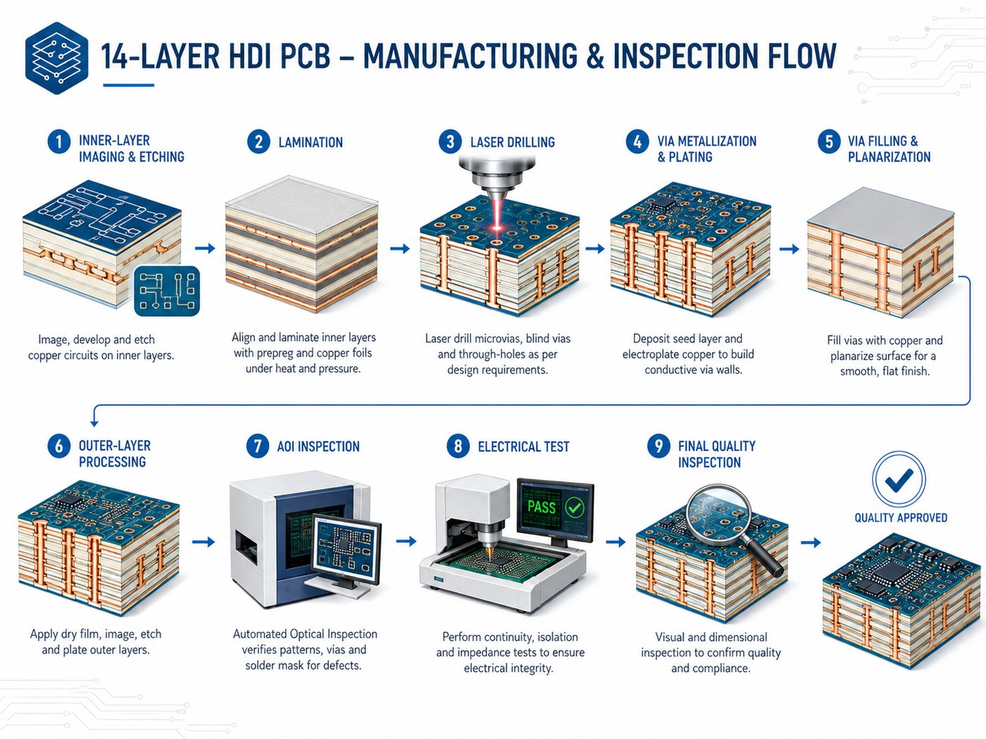
14-layer HDI PCB manufacturing and inspection flow from inner-layer imaging through laser drilling, plating, AOI and electrical test

A simplified flow is:

  • Inner-layer imaging and etching
  • AOI inspection
  • Core lamination
  • Buried-via processing if required
  • Buildup dielectric lamination
  • Laser drilling
  • Via metallization and plating
  • Via filling and planarization where required
  • Additional buildup cycles
  • Outer-layer processing
  • Solder mask and surface finish
  • Electrical and final inspection

A 2+N+2 structure repeats the buildup and laser-drilling sequence for the second HDI level.

The main manufacturing challenge is maintaining alignment and via quality through repeated processing. A factory capable of standard 14-layer PCBs is therefore not automatically qualified for complex HDI builds.

How Is 14-Layer HDI PCB Reliability Verified?

Electrical testing confirms continuity, but HDI also requires inspection of internal interconnects.

Our broader PCB testing guide explains how electrical and inspection methods complement one another.

Method Main Purpose
AOI Conductor and pattern inspection
Electrical test Open and short detection
Microsection Via plating, fill, and registration
Impedance coupon Controlled impedance verification
X-ray Selected internal structure inspection
Thermal testing Interconnect behavior under temperature stress
Dimensional inspection Alignment and finished geometry

Microsection inspection is particularly useful for stacked or filled microvias because the critical structure is hidden inside the PCB.

For high-reliability projects, define acceptance class, coupon requirements, thermal testing, and reporting requirements at RFQ stage. These items can affect both panel design and quotation.

What Affects 14-Layer HDI PCB Cost and Lead Time?

HDI architecture often affects price more than the difference between conventional multilayer counts.

Cost Driver Why It Matters
Sequential lamination Adds fabrication cycles
Stacked microvias Requires tighter registration and filling control
Fine line/space Reduces process margin
Via-in-pad filling Adds filling and planarization
Specialty laminate Raises material or sourcing cost
Tight impedance Requires engineering and verification
Additional reliability tests Adds inspection and qualification
Small prototype quantity Setup cost is spread over fewer boards

One effective way to control cost is to simplify the via structure.

If a 2+10+2 construction completes the routing, moving to 3+8+3 simply for extra flexibility is usually difficult to justify.

When comparing quotes, make sure each supplier is pricing the same material, stackup, microvia structure, surface finish, and testing requirements.

How Do You Choose a 14-Layer HDI PCB Manufacturer?

Do not qualify a supplier only by checking whether its capability table says “14 layers” or “HDI.”

Confirm the processes that your design actually requires:

  • Sequential lamination
  • Laser-drilled microvias
  • Copper-filled via-in-pad
  • Stacked or staggered microvias
  • Fine line and space
  • Controlled impedance
  • Layer registration
  • Microsection inspection
  • Electrical testing

The manufacturer’s DFM feedback should also be specific. If an engineer suggests changing a stacked microvia to a staggered one, the reason should be clear—whether it is reliability, process margin, cost, or production capability.

For quotation, provide:

  • Gerber or ODB++ data
  • Drill files
  • Preferred stackup, if available
  • Material requirement
  • Finished board thickness
  • Copper weight
  • Impedance requirements
  • Microvia and via-in-pad details
  • Surface finish
  • Test requirements
  • Prototype and production quantities

If the stackup is still open, provide the electrical and mechanical requirements instead.

At EBest Circuit, reviewing the stackup and via structure before layout is locked gives engineers more room to resolve manufacturing issues without forcing major redesign later.

Frequently Asked Questions About 14-Layer HDI PCBs

Is every 14-layer PCB an HDI PCB?

No. Fourteen layers describe the copper-layer count. HDI describes the interconnection technology. A 14-layer board can still be a conventional multilayer PCB.

What is a typical 14-layer HDI PCB stackup?

There is no universal stackup. Structures such as 1+12+1 and 2+10+2 are possible, but the final choice depends on BGA routing, impedance, board thickness, and required HDI layers.

What is the difference between a 14-layer HDI PCB and a standard 14-layer PCB?

A 14-layer HDI PCB uses localized high-density connections such as microvias and blind vias. A standard 14-layer PCB may rely mainly on through vias.

Should stacked or staggered microvias be used in a 14-layer HDI PCB?

Use stacked microvias when routing density requires vertical alignment. Use staggered microvias when enough offset space is available and the design does not require the more compact structure.

What files are required to manufacture a 14-layer HDI PCB?

Provide fabrication and drill data plus the stackup or electrical requirements, material, copper thickness, impedance targets, microvia details, via-fill requirements, surface finish, test requirements, and quantity.

How Can EBest Circuit Support Your 14-Layer HDI PCB Project?

At EBest Circuit, we support HDI PCB stackup review, DFM feedback, controlled impedance, laser-drilled microvias, and multilayer PCB fabrication. Send us your Gerber or ODB++ files, stackup, material, finished thickness, impedance targets, via structure, surface finish, test requirements, and quantities for an engineering review and quotation.

You may also like

HDI PCB Design Review: Stackup, Microvia and DFM Checks
Tuesday, July 21st, 2026

An HDI PCB is ready for fabrication only when its package escape, stackup, microvia structure, materials and release data describe one manufacturable system. The most useful design review does not ask whether each feature works in isolation. It checks whether all of those features can be built, inspected and repeated together.

HDI PCB 3D cutaway with build-up layers, microvias and fine-pitch BGA routing

This guide gives hardware designers, PCB layout engineers, quality teams and buyers a practical release sequence. It starts with the reason for using HDI, follows the design through stackup and microvia decisions, and ends with the evidence and files a fabricator needs before production.

What Is an HDI PCB, and When Does a Design Need It?

An HDI PCB is a high-density interconnect board that uses fine conductors and compact interconnect structures to route more connections within limited space. Laser-drilled microvias, blind or buried vias, via-in-pad and sequential build-up layers are common, but the presence of one feature does not automatically make HDI the right choice.

Use HDI when a measurable constraint cannot be solved cleanly with a conventional multilayer construction. Typical triggers include:

  • A fine-pitch BGA whose inner rows cannot escape through practical mechanically drilled vias.
  • A fixed board outline that leaves too few routing channels for the required nets.
  • A thickness limit that makes a larger conventional layer count unsuitable.
  • Critical connections that benefit from shorter stubs or more controlled layer transitions.

If standard through vias, sensible trace rules and an ordinary multilayer stackup can complete the design, HDI may add lamination cycles and process risk without adding product value.

Design condition Likely direction Question to close
Fine-pitch BGA blocks escape channels Evaluate HDI Which pin rows require microvia transitions?
Moderate density and enough board area Keep a conventional multilayer option open Can through vias finish the routing with margin?
Strict thickness or form-factor limit Compare build-up alternatives Can the dielectric and copper system meet the envelope?
HDI has no defined routing benefit Stop and simplify What specific constraint does HDI solve?

What Should Be Defined Before HDI PCB Design Begins?

The component field and electrical constraints should be defined before the stackup is frozen. Starting with a familiar build-up recipe can force the design into unnecessary microvia levels or leave critical BGA rows without a valid escape path.

Prepare a short constraint map that records:

  • BGA pitch, pad size, pin-row count and permitted fan-out direction.
  • Signal groups, differential pairs, clocks and sensitive analog nodes.
  • Power and ground pin distribution, current demand and thermal paths.
  • Board outline, connector positions, keepouts and mechanical height limits.
  • Target finished thickness, copper needs and controlled-impedance nets.
  • Whether via-in-pad is necessary or dog-bone fan-out remains practical.

Route a representative dense area before committing the complete board. This early escape study shows how many build-up layers are genuinely needed and whether placement changes could remove an entire lamination cycle.

How Should an HDI PCB Stackup Be Reviewed?

An HDI PCB stackup should be reviewed as a layer-by-layer connection map, not as shorthand alone. Labels such as 1+N+1 or 2+N+2 describe the number of outer build-up layers, but they do not define dielectric materials, copper thickness, via spans or finished-board tolerances.

Read the proposed construction from the outside inward and confirm every copper layer, dielectric, core, microvia span, buried structure and lamination stage.

Review item What should be confirmed Why it matters
Build-up layers Each added layer solves a documented routing or connection need Unnecessary cycles add cost and registration interfaces
Dielectrics Material family, thickness and resin behavior are agreed They influence laser drilling, lamination and impedance
Copper Base and finished copper are identified by layer Trace geometry and plating allowances depend on copper condition
Reference planes Critical signals keep a continuous return path Plane changes can create return discontinuities
Via spans Every laser, buried and through-hole span matches the construction Ambiguous spans cause CAM questions or invalid connections
Finished thickness Nominal thickness and tolerance include the complete build Core values alone do not define the finished board

Ask the fabricator to return a proposed production stackup before final impedance routing. A late dielectric substitution can change the required trace width, spacing and coupling geometry.

HDI PCB stackup cross-section showing build-up dielectrics and adjacent-layer microvias

Which Microvia Structure Should an HDI PCB Use?

An HDI PCB should use the simplest microvia structure that completes the required layer transitions. A single adjacent-layer microvia usually introduces fewer process interfaces than a multi-level stacked structure, while staggered microvias avoid placing several plated interfaces directly above one another.

Stacked microvias can be necessary when escape space is extremely limited, but they require explicit agreement on via filling, target-pad geometry, plating and reliability validation. IPC has warned the electronics industry about latent failures in some complex microvia structures, so a room-temperature continuity test should not be treated as universal proof of long-term reliability.

  • Identify every laser-drilled, mechanically drilled, blind, buried and through-hole feature.
  • State which microvias require filling and capping for via-in-pad assembly.
  • Avoid stacked levels unless the package escape or connection path requires them.
  • Match microvia depth to the selected dielectric and the fabricator’s qualified process.
  • Define coupon and thermal-stress expectations for reliability-sensitive products.

The PCB via types guide provides a broader comparison of through, blind, buried and microvia structures.

What HDI PCB Design Guidelines Should Be Confirmed with the Fabricator?

HDI PCB design guidelines should be confirmed for the actual material, copper condition, layer role and via process. A generic minimum-rule table cannot show how several difficult features interact in one design.

Close these items before final routing:

  • Trace width and spacing by layer and copper thickness.
  • Laser via diameter, target pad, capture pad and permitted depth.
  • Via-to-copper, via-to-via and via-to-edge clearances.
  • Annular-ring and registration allowances for mechanically drilled holes.
  • Via-in-pad filling, planarization and surface-finish requirements.
  • Solder-mask definition around fine-pitch component pads.
  • Copper-density and balancing expectations in dense areas.

Do not combine every published minimum in the same location. A layout that simultaneously uses the smallest trace, spacing, pad and most complex via structure can be substantially harder to manufacture than one with a single controlled challenge.

How Should BGA Escape and Layer Transitions Be Planned?

BGA escape should be planned by pin function, routing layer and return-current path. The shortest geometric route is not necessarily the best electrical route if a layer transition leaves the signal without a nearby reference connection.

  • Assign outer rows, inner rows, power pins and ground pins before detailed fan-out.
  • Keep critical nets referenced to continuous planes where practical.
  • Place an intentional return path near signals that change reference planes.
  • Maintain differential-pair symmetry through the pad and via field.
  • Review antipad patterns for power-plane neck-down and current crowding.
  • Use the proposed production stackup for impedance calculations.

Large processors and FPGAs require a combined signal- and power-integrity review. Dense escape routing may create enough voiding to fragment a plane even when every individual clearance passes the design rules.

Fine-pitch BGA escape routing with microvias and nearby ground return vias on an HDI PCB

How Do Materials, Copper and Thermal Requirements Affect an HDI PCB?

Materials, copper and thermal requirements affect whether the selected build-up can survive fabrication and assembly while meeting electrical performance. Review dielectric thickness, reinforcement, resin behavior, copper profile and finished copper as a coordinated material set.

A lower-loss laminate is not automatically the best option for every HDI layer. The material must also support laser drilling, resin removal, copper adhesion and the planned lamination sequence. Hybrid constructions need additional attention because different material families may move differently during processing.

Thermal analysis should distinguish signal microvias from deliberate heat-transfer structures. Check how heat moves from component pads into planes, filled thermal vias, copper areas, heat spreaders and the enclosure. Do not assume that a dense field of small electrical microvias replaces a designed thermal path.

How Does the HDI PCB Manufacturing Process Affect Design Decisions?

The HDI PCB manufacturing process affects design because each build-up level adds drilling, metallization, imaging, lamination and registration work. The exact route depends on the via map and layer sequence, so the drawing must describe the construction rather than simply state “HDI.”

  1. Fabricate and inspect the inner core or sub-composite.
  2. Create buried interconnects that must be completed before the next lamination.
  3. Laminate the next dielectric and copper layer.
  4. Laser-drill the specified microvias and prepare the hole surfaces.
  5. Metallize, plate and fill the vias required by the design.
  6. Image and etch the added circuit layer.
  7. Repeat the build-up sequence when more HDI levels are necessary.
  8. Complete outer-layer processing, solder mask, surface finish and profiling.
  9. Perform electrical testing and the agreed inspection or coupon evaluation.

Each repeated cycle creates another opportunity for dimensional movement and registration error. A design that removes an unnecessary build-up level can improve manufacturability without changing the product function.

What DFM Evidence and Quality Data Should Be Reviewed?

A useful DFM review should return specific findings tied to the artwork, stackup and via structure. A generic pass/fail message does not show whether manufacturing assumptions match the design intent.

  • Confirm the production stackup and impedance construction returned by CAM.
  • Review separate drill information for laser, blind, buried and through structures.
  • Check target pads, capture pads, annular rings and solder-mask findings.
  • Review local copper density, plane clearances and copper balancing.
  • Agree on test coupons, microsection locations and acceptance criteria.
  • Define electrical-test coverage and any resistance-monitoring requirement.
  • Record approved exceptions so prototype and production use the same decision basis.

IPC-6012F covers qualification and performance requirements for rigid printed boards and gives expanded attention to microvia structures. The applicable class, revision, customer specification and acceptance plan should be stated in the procurement documentation rather than assumed.

Use the broader PCB design for manufacturability checklist alongside this HDI-specific review.

Laboratory microsection inspection of plated and filled HDI PCB microvias

Which HDI PCB Risks Should Stop a Production Release?

A production release should stop whenever the construction cannot be described unambiguously or a risk spans design, fabrication and assembly. Resolving these issues before quotation is usually faster than answering repeated CAM questions after purchase order release.

Stop condition Likely consequence Required correction
A microvia span does not match the stackup Invalid or unintended layer connection Correct the via map and drill data
Stacked microvias have no validation plan Latent interface risk may be missed Review the structure, coupons and stress criteria
Impedance uses a placeholder dielectric Production geometry changes after routing Approve the proposed material stackup first
Fine-pitch pads conflict with mask capability Missing mask dams or exposed copper Review pad definition with fabrication and assembly
A dense via field fragments a power plane Higher path impedance or local current crowding Rework the fan-out and plane copper
The drawing says only “HDI” Filling, lamination and acceptance remain undefined Add explicit construction and process notes

What Files Should Be Included in an HDI PCB Release Package?

An HDI PCB release package should allow the fabricator to reconstruct the intended build without guessing from artwork. Use one revision across the manufacturing data, drawings and supporting notes.

  • Gerber, ODB++ or IPC-2581 manufacturing data.
  • NC drill files separated by drill type where appropriate.
  • A complete layer stackup with dielectric, copper and finished-thickness requirements.
  • A via map showing every blind, buried, microvia and through-hole span.
  • A fabrication drawing with dimensions, tolerances, finish and acceptance notes.
  • An impedance table tied to layer numbers and net classes.
  • A netlist or other data required for electrical testing.
  • A release readme that identifies the authoritative revision and approved exceptions.

For assembly quotation, include the BOM, centroid or pick-and-place file, assembly drawings, special process notes and expected quantity. Fabrication and assembly data must refer to the same board revision.

How Should an HDI PCB Design Review Checklist Be Used?

An HDI PCB design review checklist should be used as a release gate, not as paperwork completed after the files are sent. Assign an owner to every open item and do not release production data until the construction-critical questions are closed.

Review area Release requirement
Need for HDI The design documents which routing, size or electrical constraint requires HDI
Package escape BGA fan-out, power pins and return paths have been reviewed together
Stackup The material set, build-up sequence and finished thickness are approved
Microvias Spans, filling, stacking and pad geometry are explicit
Design rules Trace, spacing, pad, mask and clearance rules match the selected process
Electrical behavior Impedance and power-integrity work use the proposed production stackup
Reliability Applicable requirements, coupons and inspection criteria are agreed
Release data Artwork, drills, drawings, netlist and revision notes are complete
DFM closure Every CAM exception has an owner and recorded disposition

What Questions Do Engineers and Buyers Ask About HDI PCB?

Is every fine-pitch BGA board an HDI PCB?

No. Package pitch is only one input. Pin-row count, board area, layer availability, pad geometry and routing demand determine whether microvias or sequential build-up layers are necessary. Complete a representative escape study before selecting the construction.

What is the difference between HDI and a conventional multilayer PCB?

A conventional multilayer board commonly relies on mechanically drilled through holes and a simpler lamination route. HDI uses finer interconnect features, often including laser microvias and sequential build-up layers. The practical difference is routing density and process complexity, not layer count alone.

Does an HDI PCB always cost more?

Its fabrication route is usually more complex, but the product-level comparison depends on the design. HDI may reduce board area or avoid additional conventional layers. Compare the complete board, assembly and reliability plan rather than applying one price multiplier.

Are staggered microvias always preferable to stacked microvias?

Staggered microvias are often preferred when space allows because they avoid a direct vertical stack of plated interfaces. Stacked microvias remain useful for very dense connections, but filling, plating and reliability validation require closer control.

When should via-in-pad be used?

Use via-in-pad when component pitch leaves no practical space for dog-bone fan-out or when a short electrical or thermal path is required. The fabrication drawing should define filling and capping so the assembled pad remains flat and solderable.

Can the impedance stackup be finalized after routing?

It should be coordinated before final routing. Production dielectric thickness, copper thickness and copper profile affect the required geometry. A late stackup change may force trace-width and spacing revisions across the board.

Which standards are commonly referenced for HDI design and acceptance?

IPC-2226 is commonly referenced for HDI design, while the IPC-6012 family addresses qualification and performance requirements for rigid printed boards. Purchase documents should identify the applicable revision, class, addenda and customer-specific requirements.

How should microvia reliability be verified?

The plan depends on product risk and via structure. Electrical testing, microsection evaluation, test coupons and thermal-stress or reflow-simulation methods may be appropriate. Complex stacked structures should be reviewed with the fabricator and customer before acceptance criteria are frozen.

What causes the most HDI PCB quotation delays?

Ambiguous stackups, missing via-span definitions, conflicting drill tables, undefined via filling, incomplete impedance information and mismatched file revisions are common causes. A single release readme and clear via map prevent many avoidable questions.

Should prototype and production HDI boards use the same construction?

Use the same critical stackup, via architecture and acceptance basis when the prototype is intended to validate production behavior. A simplified prototype may confirm circuit function, but it cannot validate a different production interconnect structure.

How Can EBest Circuit Review Your HDI PCB Before Fabrication?

Begin with a complete stackup, via map and manufacturing dataset. EBest Circuit can review HDI PCB data for stackup feasibility, microvia structure, impedance requirements and fabrication questions. Send the Gerber or ODB++ package, fabrication drawing, target thickness, quantity and application requirements through the BestPCBs contact page for engineering review and quotation.
You may also like