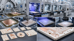
Quick turn DPC ceramic PCB fabrication explained for engineers: materials, process, tolerances, testing, failure risks, cost, and supplier selection.
What Is Quick Turn DPC Ceramic PCB Fabrication?
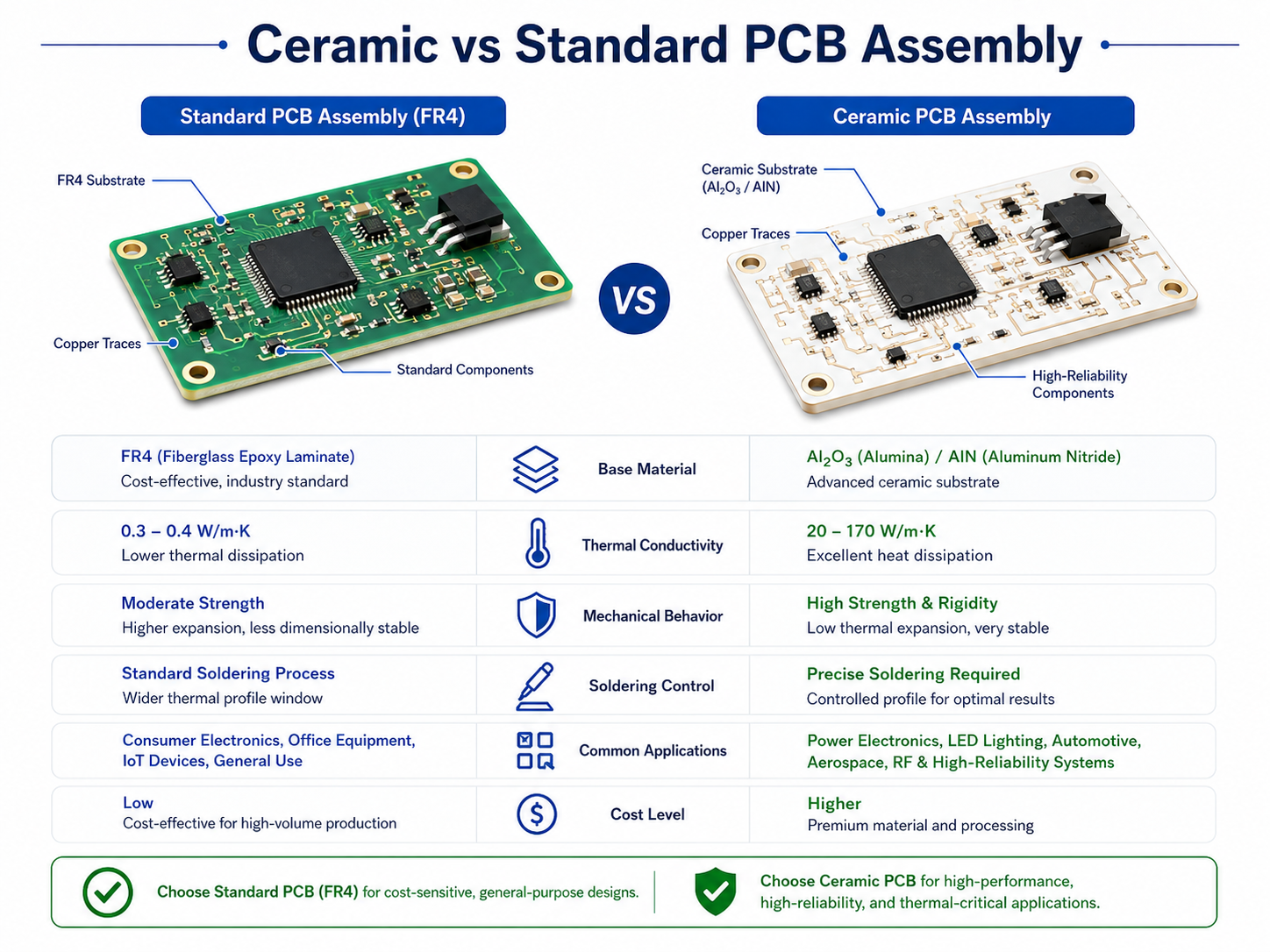
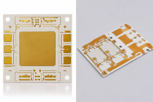
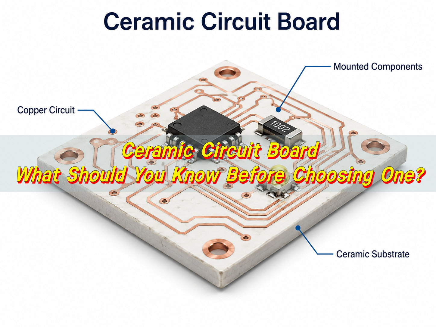
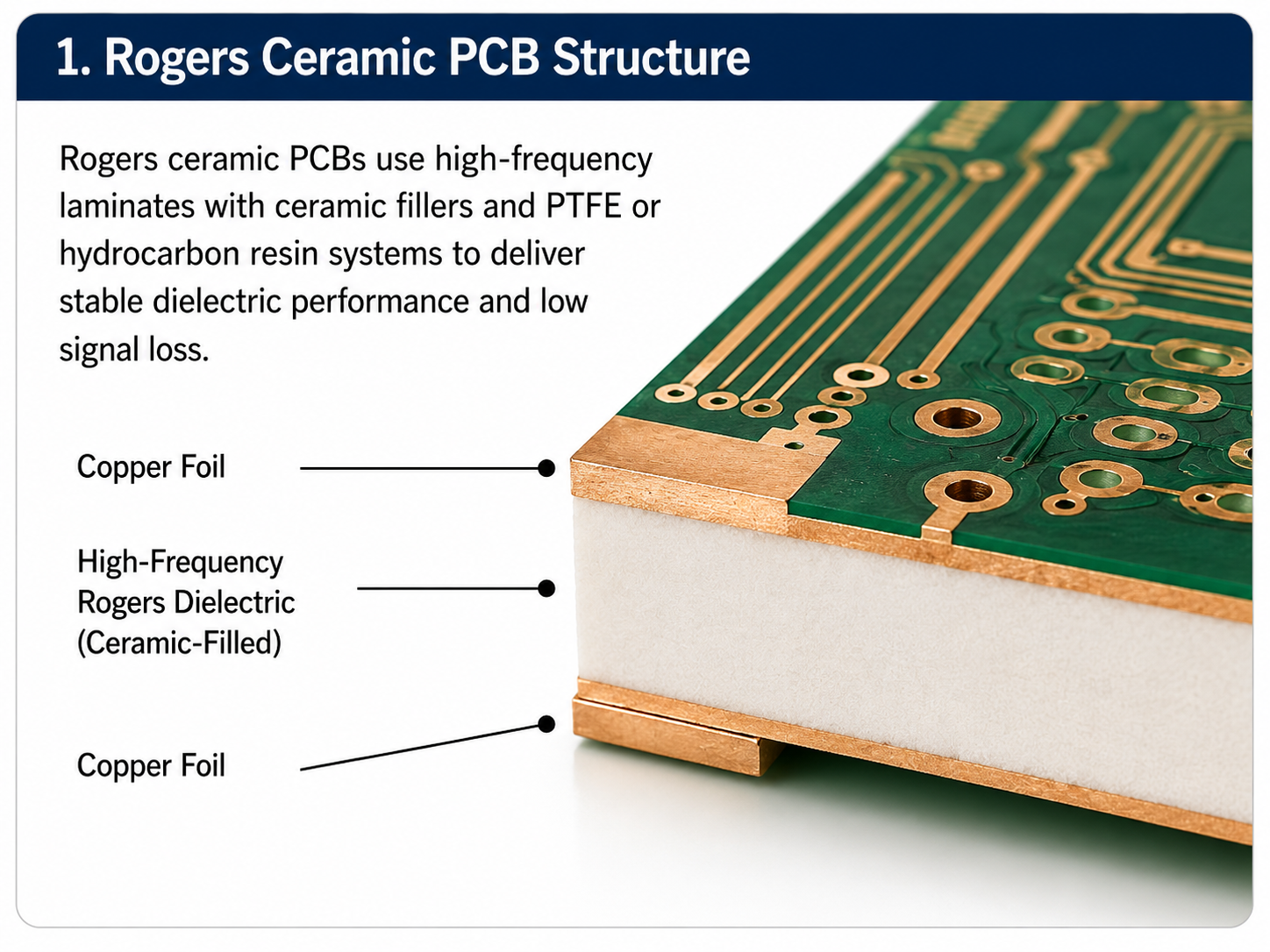
Quick turn DPC ceramic PCB fabrication refers to the fast manufacturing of ceramic circuit boards using Direct Plated Copper technology. In electronics manufacturing, DPC means Direct Plated Copper or Direct Plating Copper, where copper is deposited directly onto a ceramic substrate instead of using standard FR4 laminate construction.
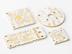
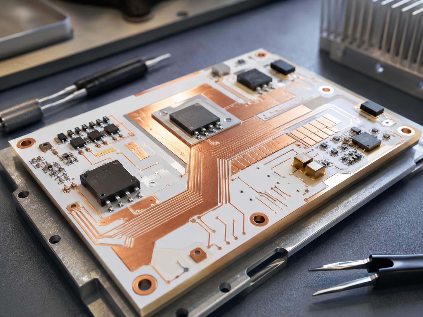
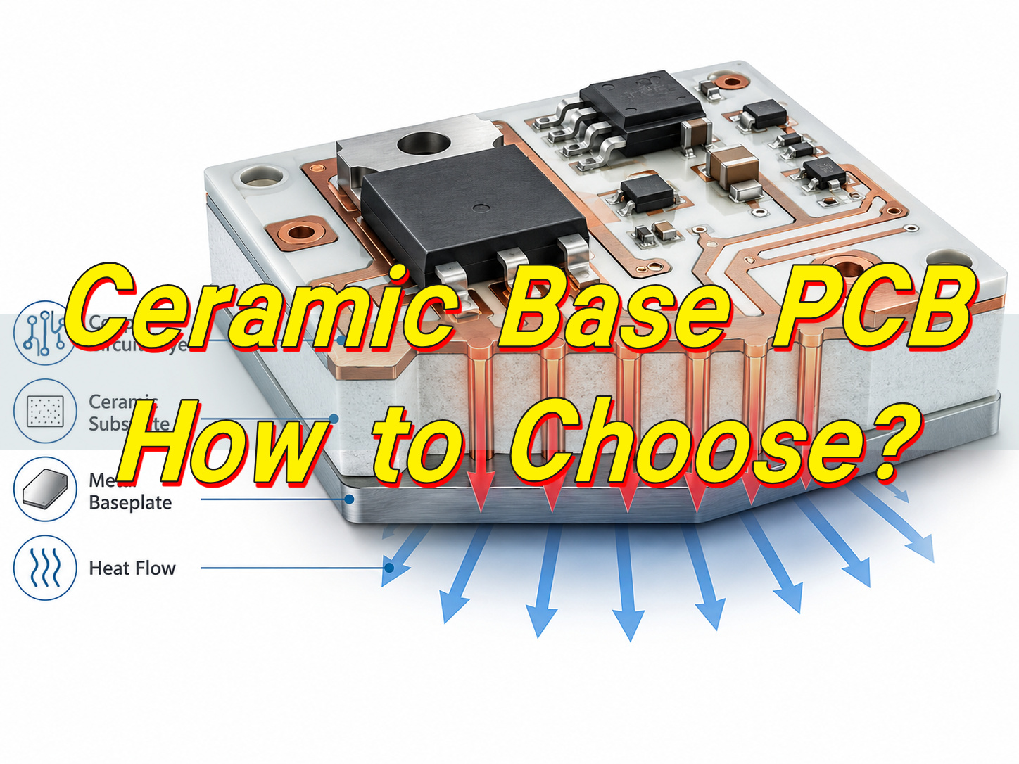
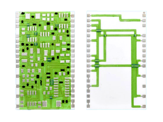
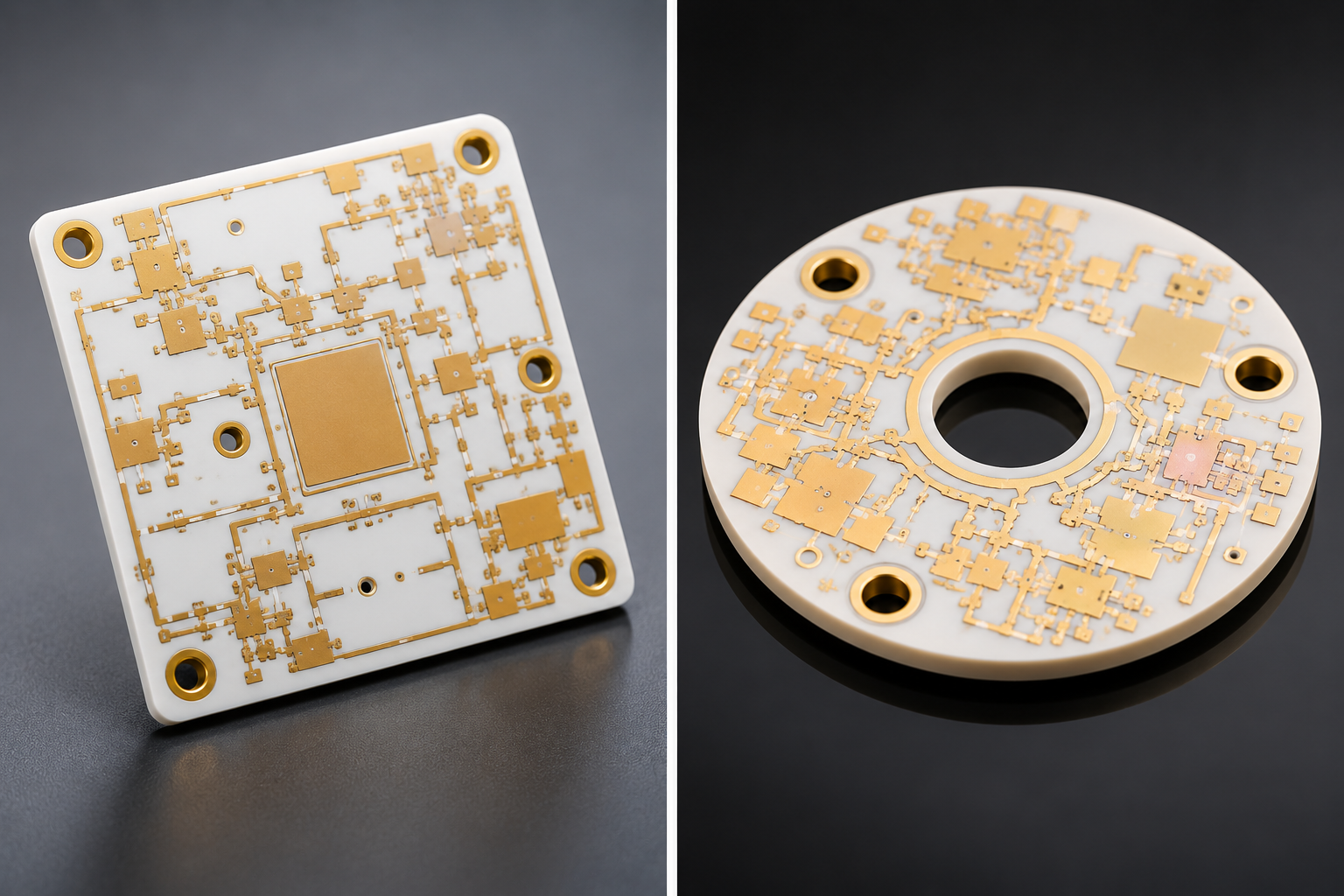
A DPC ceramic PCB usually uses alumina, aluminum nitride, or other ceramic materials as the insulating base. A thin metal seed layer is first formed on the ceramic surface, then copper is built up by electroplating. This makes the process suitable for fine circuits, good surface flatness, high thermal performance, and compact power modules. Some manufacturers describe DPC as a thin-film ceramic PCB process improved by copper plating.
For quick turn projects, the goal is not only fast delivery. The real goal is fast engineering validation without sacrificing adhesion, line accuracy, insulation performance, surface finish quality, or thermal reliability.
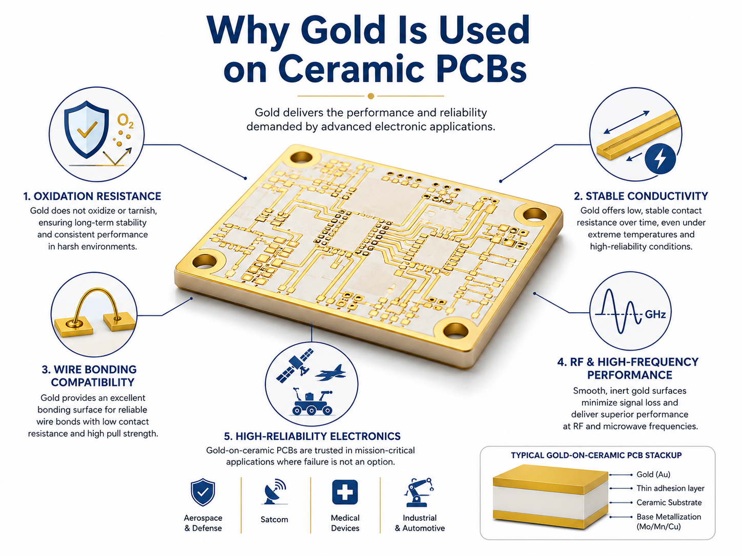
Why Is DPC Ceramic PCB Important for High-Power Electronics?
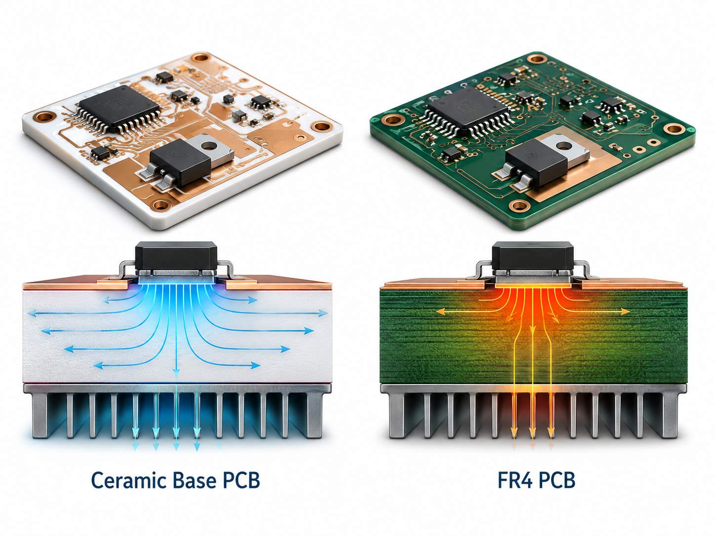
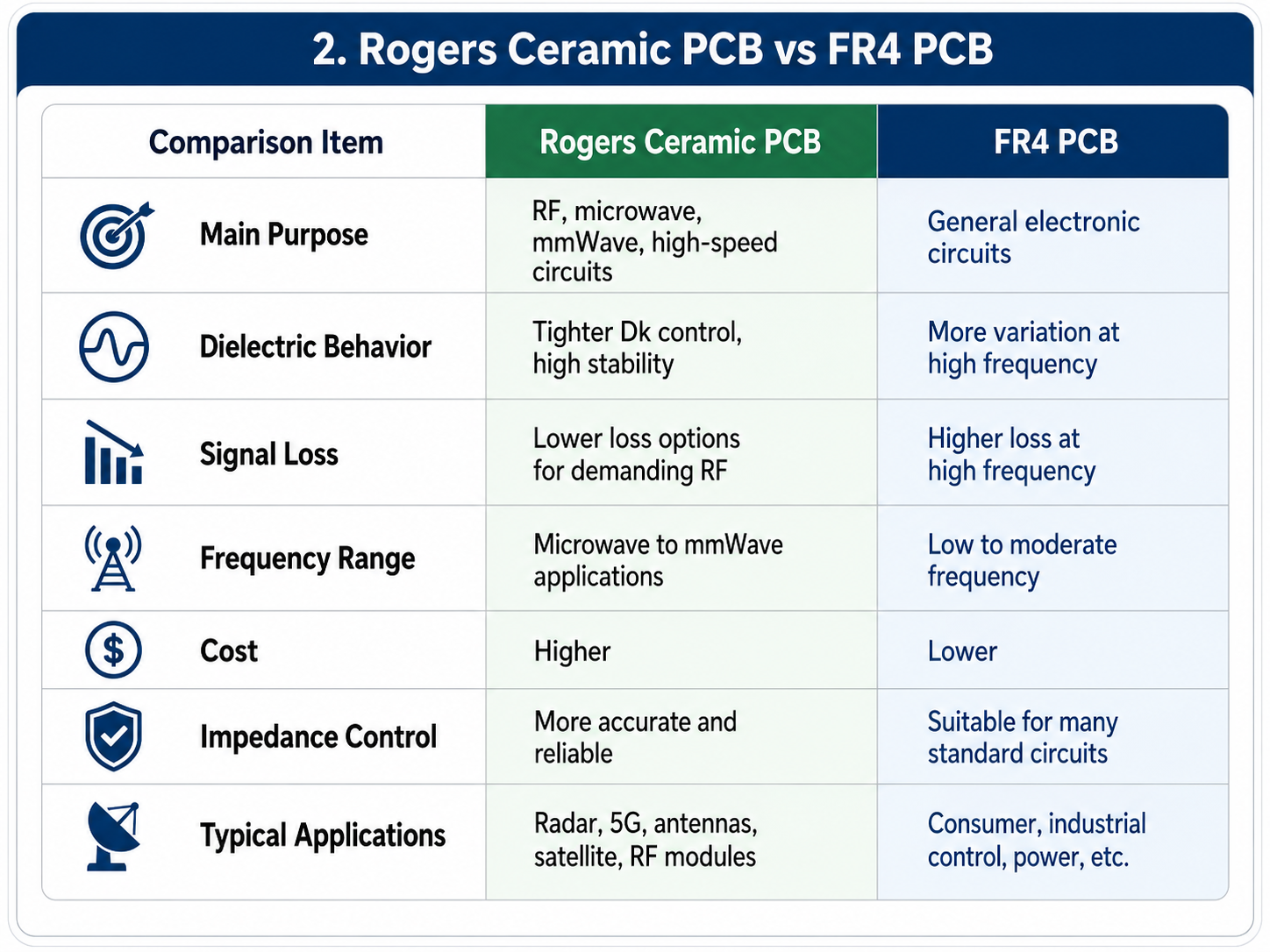
DPC ceramic PCB is important because many modern electronic products generate more heat in smaller spaces. FR4 can work well for general electronics, but it has practical limits when heat density, dielectric strength, thermal expansion, and long-term stability become critical.
DPC ceramic PCB fabrication helps solve several engineering problems:
| Engineering Need | Why DPC Ceramic PCB Helps |
|---|---|
| Heat dissipation | Ceramic substrate transfers heat more efficiently than FR4 |
| Fine circuit routing | Plated copper supports fine patterns and compact layouts |
| Electrical insulation | Ceramic provides strong dielectric performance |
| Dimensional stability | Ceramic has low expansion under heat |
| Power density | Suitable for LEDs, power modules, sensors, and RF devices |
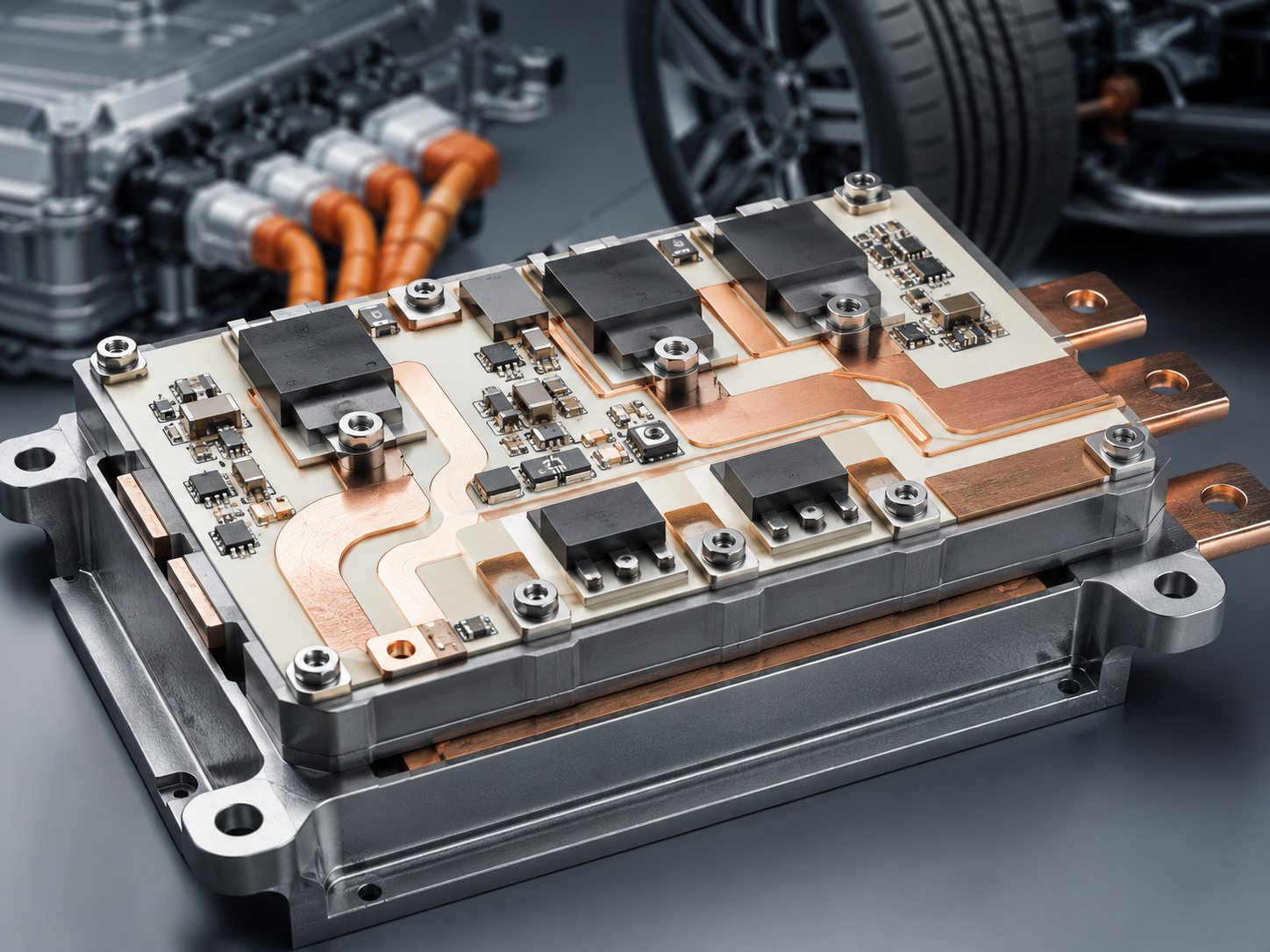
For products using high-power LEDs, laser diodes, SiC/GaN devices, high-current drivers, power sensors, medical modules, automotive lighting, and industrial control electronics, the substrate often becomes part of the thermal design, not just a carrier for copper traces.
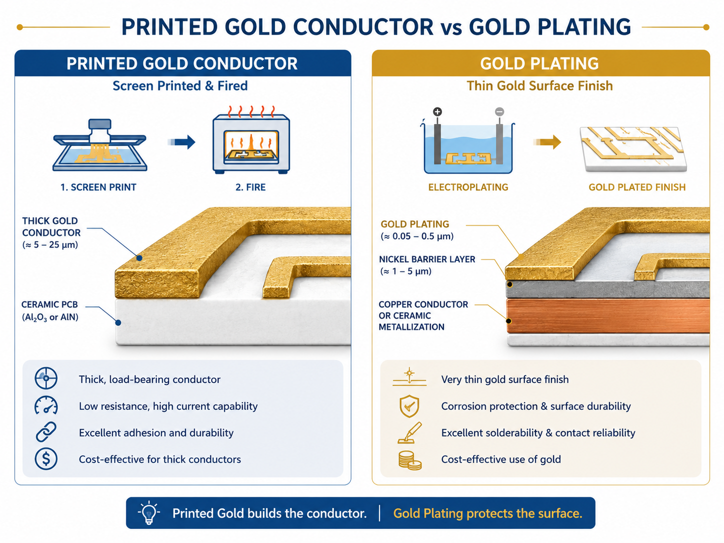
How Does Direct Plated Copper Work?
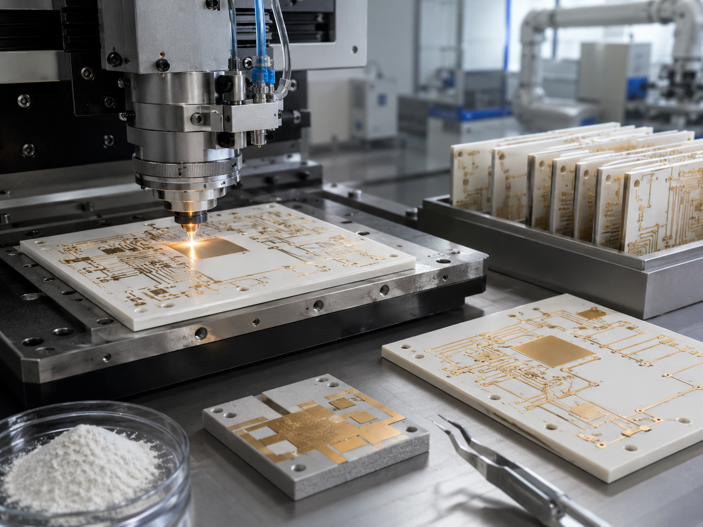
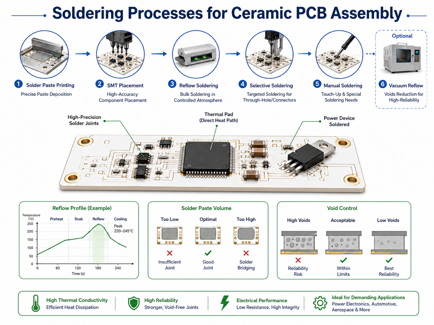
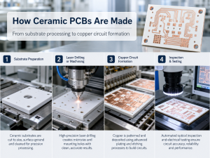
DPC manufacturing starts with a ceramic substrate. The surface is cleaned and prepared, then a very thin adhesion or seed layer is deposited. Titanium, copper, or similar metallization structures may be used depending on the process route. After that, copper is electroplated to the required thickness, patterned, etched, finished, and inspected.
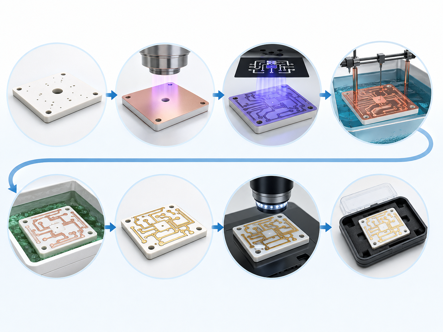
A typical DPC ceramic PCB process includes:
- Ceramic substrate selection
- Laser drilling or mechanical processing
- Surface cleaning and activation
- Thin-film sputtering or seed-layer formation
- Photoresist coating
- Exposure and development
- Copper electroplating
- Circuit etching
- Surface finish
- Electrical test
- AOI and dimensional inspection
- Packaging for shipment
The key difference from thick-film ceramic circuits is that DPC builds copper through plating instead of screen-printing conductive paste. Compared with DBC, it is usually better for finer line width, smaller pads, and precision circuit patterns. DPC is often described as close to standard PCB design logic because copper thickness can be controlled by plating after a seed layer is formed.
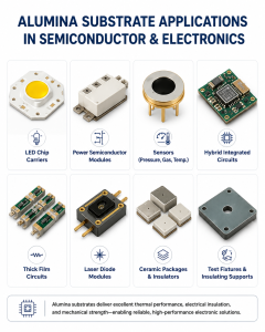
Which Materials Are Used for DPC Ceramic PCB Fabrication?
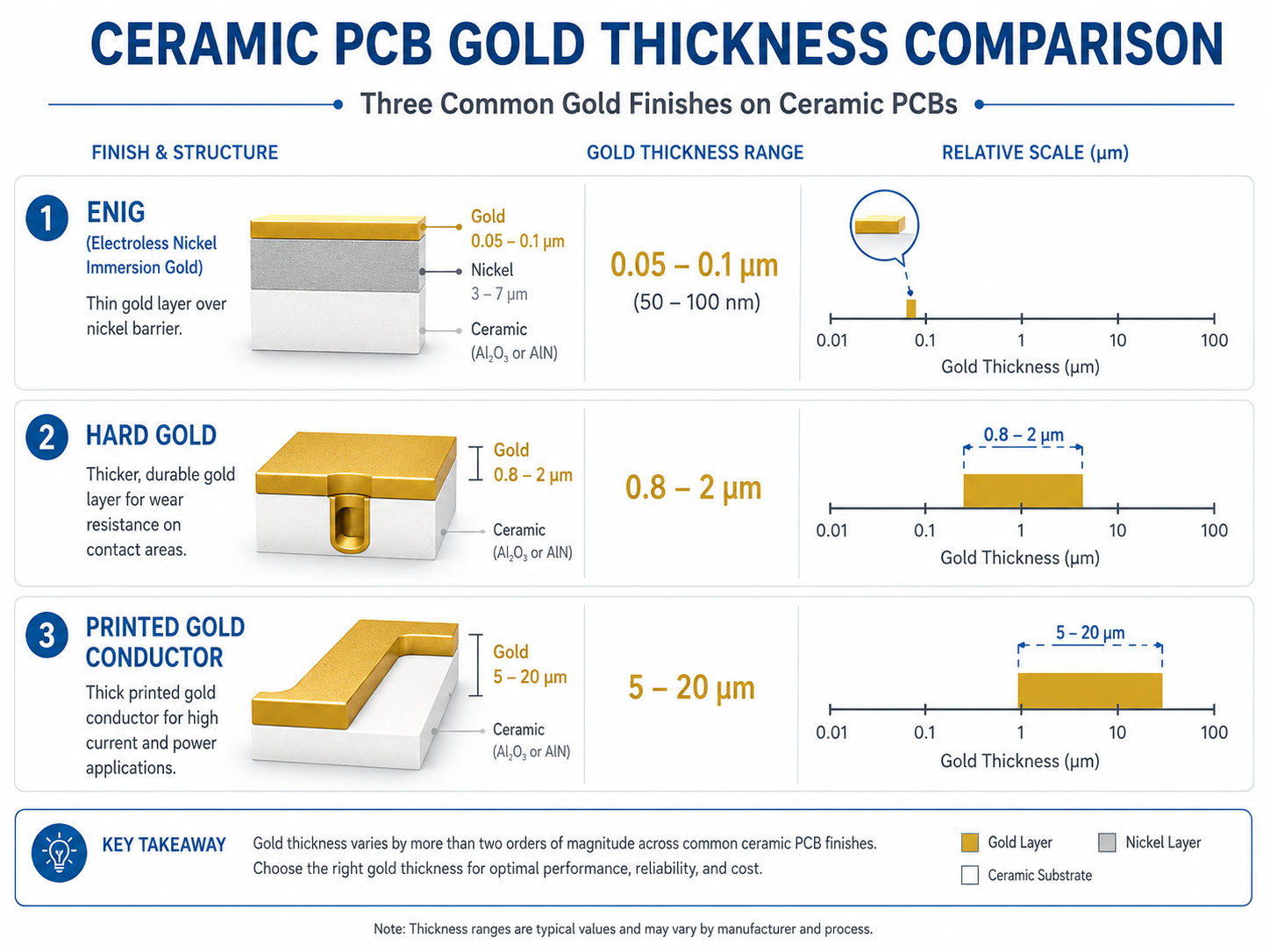
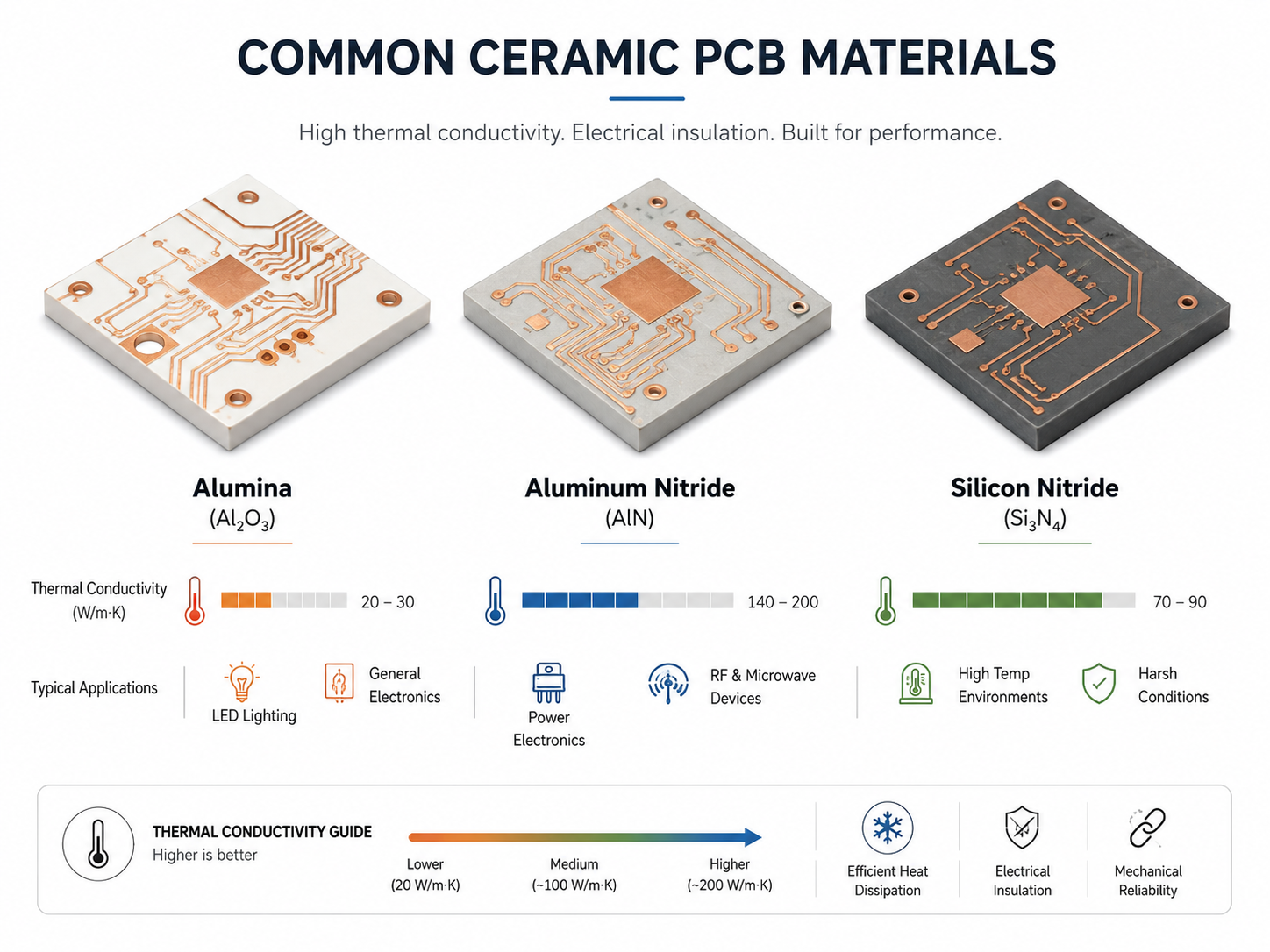
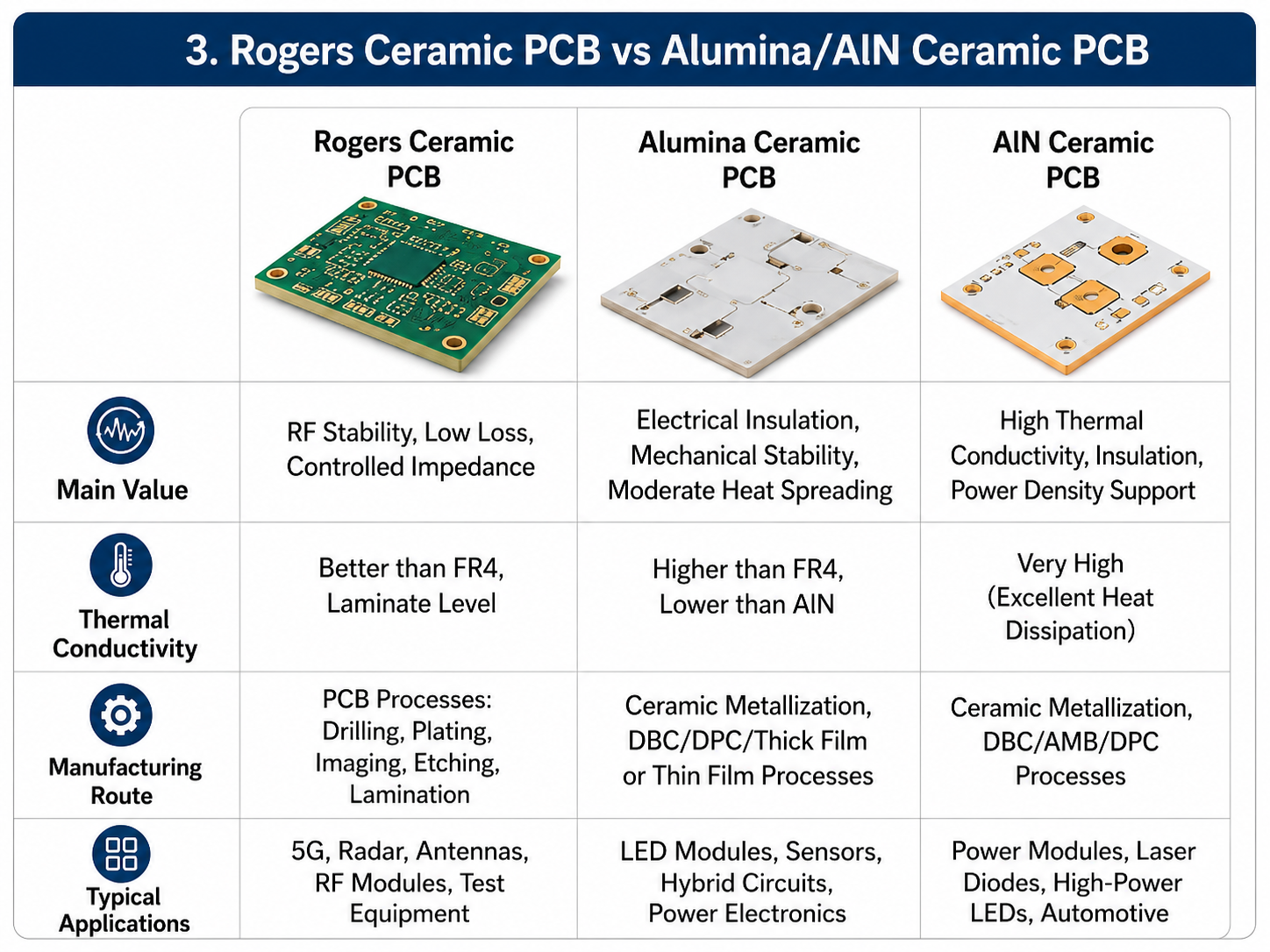
The most common substrate materials for DPC ceramic PCB are alumina and aluminum nitride. The right choice depends on heat, cost, mechanical strength, insulation, and application environment.
| Material | Common Use | Main Strength |
|---|---|---|
| Alumina, Al₂O₃ | LED modules, sensors, industrial electronics | Cost-effective ceramic insulation |
| Aluminum Nitride, AlN | High-power LEDs, power modules, laser systems | High thermal conductivity |
| Silicon Nitride, Si₃N₄ | High-reliability power electronics | Strong mechanical toughness |
| Zirconia-based ceramics | Special mechanical or insulating uses | High strength and wear resistance |
Aluminum nitride is widely used when thermal conductivity is a dominant requirement. Kyocera describes AlN as a material with high thermal conductivity and electrical insulation, used in heat-dissipating and heat-soaking components. MARUWA also highlights AlN for high thermal conductivity, electrical insulation, and a coefficient of thermal expansion close to silicon, making it useful for power modules and LEDs.
For most buyers, alumina is the practical starting point when cost matters. AlN becomes more attractive when junction temperature, power density, or device lifetime requires better heat transfer.
DPC vs DBC vs Thick Film Ceramic PCB
DPC, DBC, and thick film are all ceramic circuit technologies, but they serve different design needs.
| Process | Best Fit | Main Advantage | Common Limitation |
|---|---|---|---|
| DPC | Fine circuits, compact pads, prototype validation | Precise pattern, good flatness | Higher process control requirement |
| DBC | High-current power modules | Thick copper, strong current capacity | Less suitable for very fine traces |
| Thick Film | Resistors, sensors, hybrid circuits | Mature and flexible | Conductive paste performance varies |
| LTCC/HTCC | Multilayer ceramic modules | Integrated ceramic package design | Longer development cycle |
DPC is often the better choice when engineers need fine trace geometry, plated copper, ceramic heat dissipation, and quick prototype production. DBC is often selected for high-current power substrates where thicker copper is more important than fine routing. Thick film is useful for hybrid circuits, printed resistors, and sensor modules.
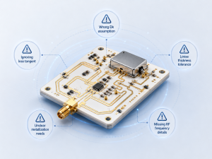
For quick turn DPC ceramic PCB fabrication, the design should stay realistic. Very thick copper, complex multilayer ceramic stacks, extremely tight spacing, and unusual surface finishes can extend lead time.
Key Specifications Engineers Should Confirm Before Fabrication
Before placing a quick turn order, confirm the specifications that directly affect manufacturability, cost, and reliability.
| Specification | What to Confirm |
|---|---|
| Ceramic material | Al₂O₃, AlN, Si₃N₄, or other |
| Substrate thickness | Commonly selected by heat, strength, and package height |
| Copper thickness | Match current, heat, and etching capability |
| Line width and spacing | Confirm with manufacturer before layout release |
| Hole type | Laser hole, metallized hole, or non-plated hole |
| Surface finish | ENIG, immersion silver, OSP, or custom finish |
| Solder mask | Required or not required |
| Warpage control | Important for assembly and module bonding |
| Thermal path | Pad-to-ceramic-to-heatsink structure |
| Test method | E-test, AOI, adhesion check, insulation test |
A common mistake is sending only Gerber files without explaining power load, device package, operating temperature, insulation requirement, or assembly method. DPC ceramic PCB fabrication is highly connected with final use conditions, so the manufacturer needs more than a drawing.
Advantages of Quick Turn DPC Ceramic PCB
Quick turn DPC ceramic PCB fabrication gives engineers a faster way to validate high-thermal designs before committing to batch production.
The main advantages include:
- Faster prototype validation
- Better heat spreading than standard FR4
- Fine circuit pattern capability
- Good surface flatness for chip mounting
- Strong electrical insulation
- Stable performance under heat
- Suitable for compact power designs
- Easier transition from prototype to small batch
For R&D teams, quick turn service is valuable when the design still needs verification. It allows engineers to test solderability, thermal performance, die attach behavior, pad geometry, electrical isolation, and mechanical fit before releasing a production build.
The strongest value appears in projects where one failed thermal design can delay the whole product schedule. A well-made DPC prototype helps shorten that risk loop.
Limitations and Design Boundaries of DPC Ceramic PCB
DPC ceramic PCB is not a universal replacement for FR4, aluminum PCB, or DBC substrate. It has clear boundaries.
DPC may not be the best option when:
- The product only needs low-cost signal routing
- The board area is large and mechanically exposed
- The design requires heavy copper beyond practical plating limits
- The circuit needs complex multilayer routing
- Mechanical shock is severe and ceramic cracking risk is high
- The application does not need ceramic-level thermal performance
Ceramic is hard and stable, but it is also brittle compared with organic laminates. Layout, mounting holes, edge distance, screw pressure, fixture design, and packaging must be reviewed carefully. Many ceramic PCB failures are not caused by the circuit itself. They come from mechanical stress, poor thermal interface design, wrong panel handling, or unsuitable assembly fixtures.
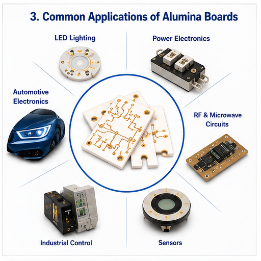
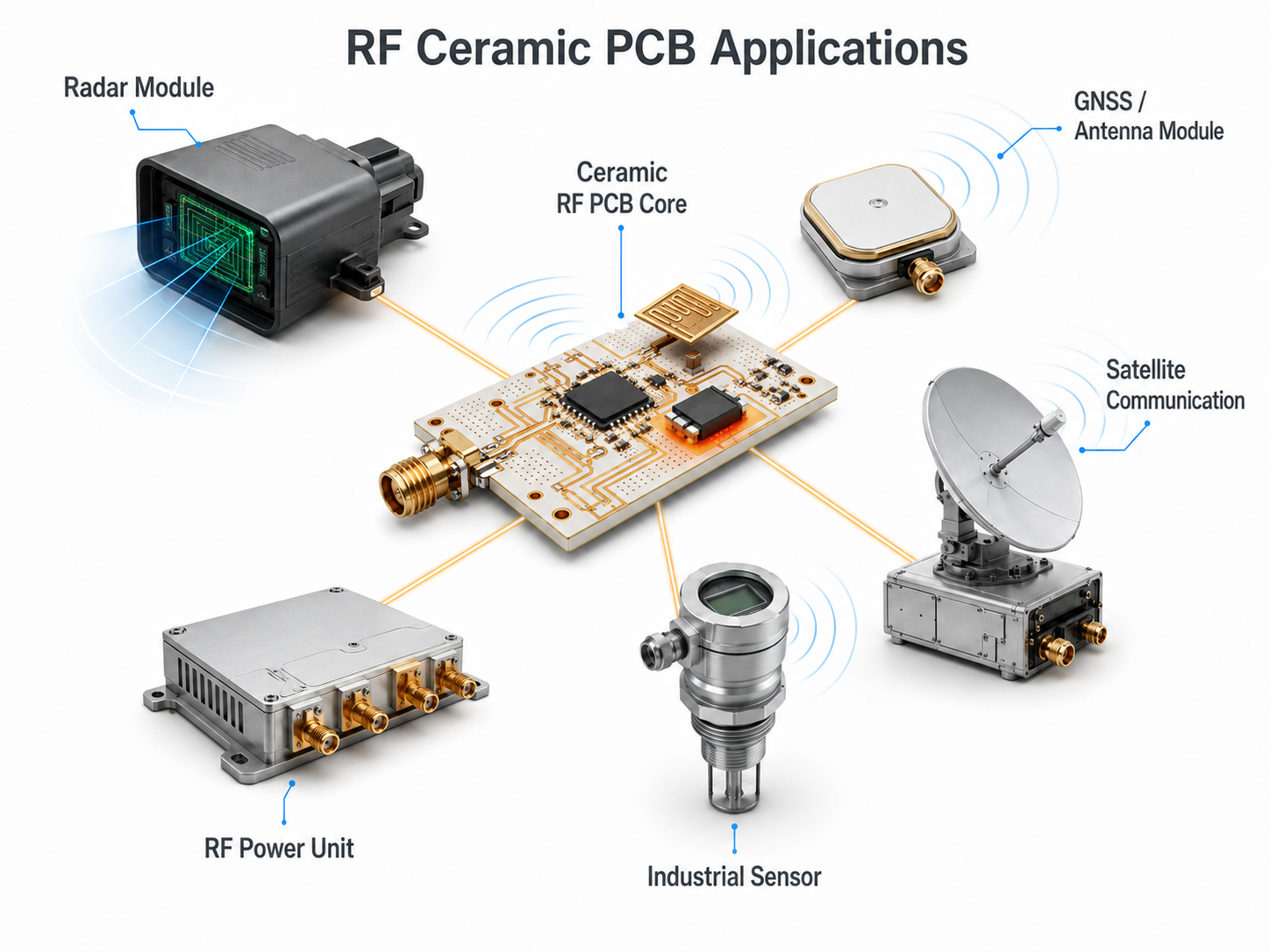
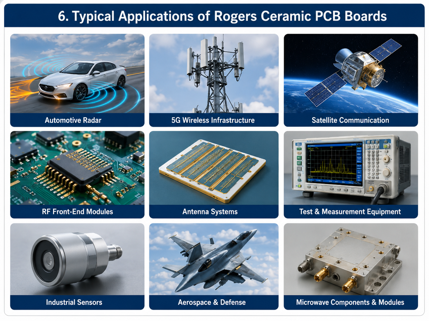
Where Are DPC Ceramic PCBs Used?
DPC ceramic PCBs are widely used in electronic products that need compact routing, fast heat transfer, and stable insulation.
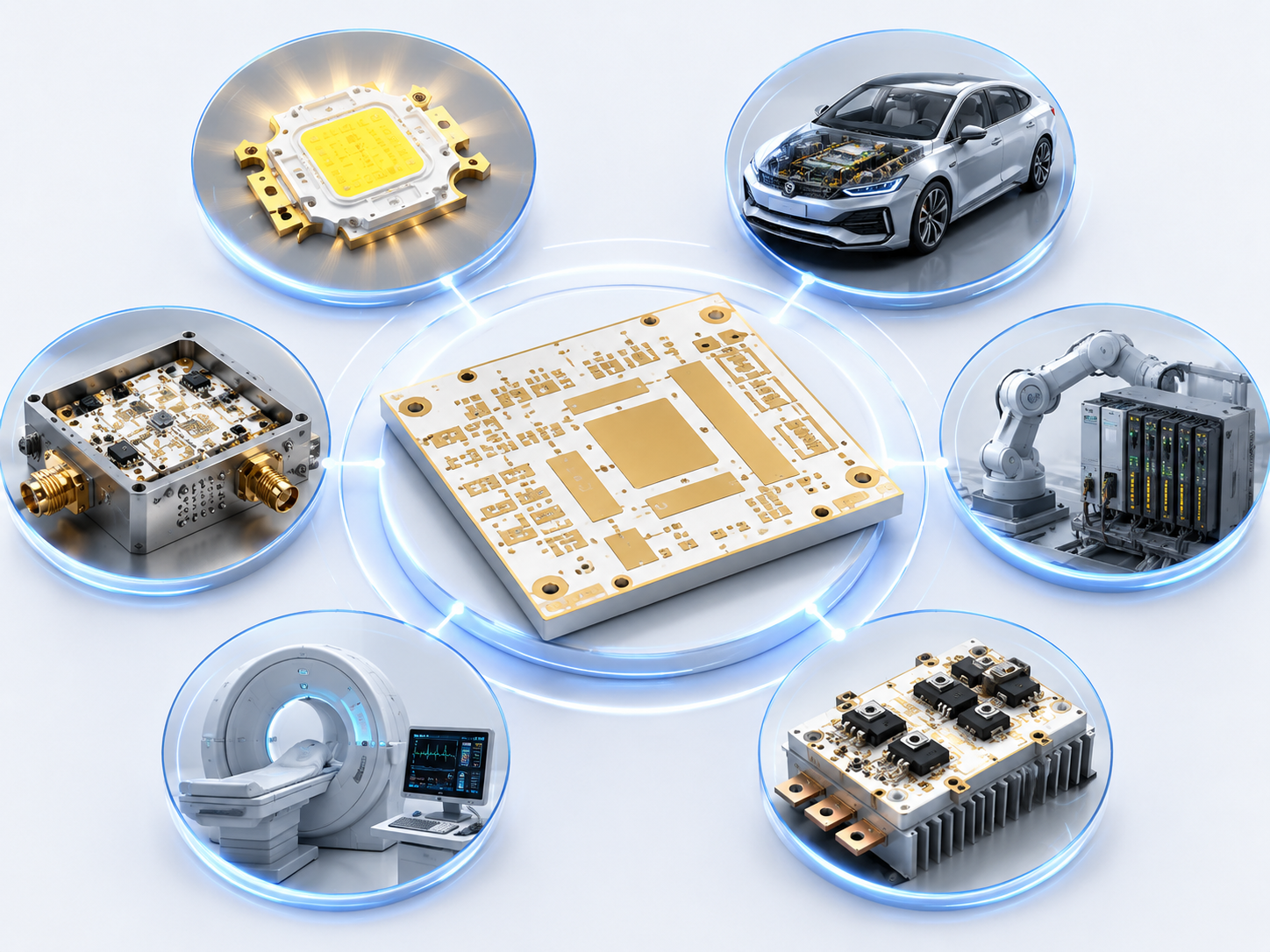
Common applications include:
- High-power LED modules
- UV LED curing systems
- Laser diode modules
- Automotive lighting
- EV power electronics
- SiC and GaN driver circuits
- Power sensors
- Semiconductor test modules
- Medical electronics
- RF and microwave modules
- Industrial control electronics
- Optical communication devices
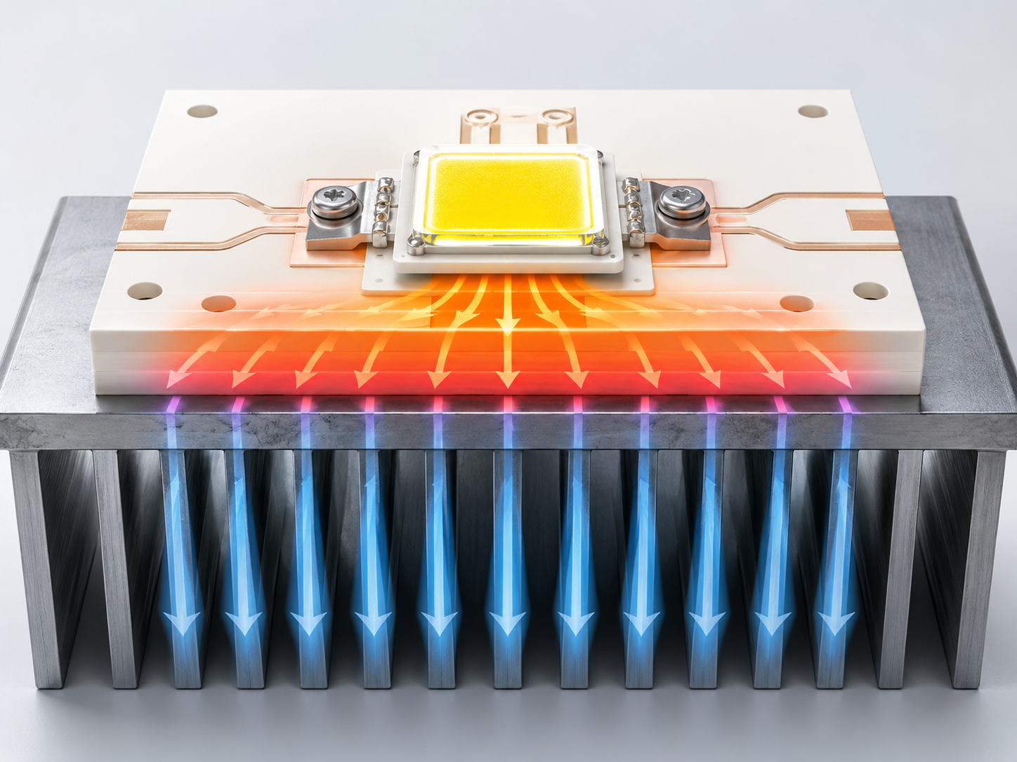
In high-power LED projects, DPC ceramic PCB helps conduct heat away from the LED junction. In laser modules, it supports compact pads and stable heat spreading. In power electronics, it can serve as a high-insulation substrate for compact power devices.
For U.S. and European buyers, key concerns often include RoHS compliance, long-term reliability, documentation, and repeatable production quality. RoHS rules restrict hazardous substances in electrical and electronic equipment, and many electronics buyers require clear material and surface finish compliance records before approval.
Practical Engineering Case: High-Power LED Ceramic Substrate
A high-power LED module may fail early if the thermal path is too slow or uneven. In one typical project, the LED package, solder layer, copper pad, ceramic substrate, thermal interface material, and heatsink all form one heat-transfer chain.
For this type of project, engineers should review:
- LED junction temperature target
- Copper pad size
- Ceramic material selection
- Solder void control
- Surface finish compatibility
- Heatsink contact flatness
- Mounting pressure
- Thermal interface material thickness
If alumina cannot keep the temperature within the design target, AlN may be selected. If copper thickness is not enough for current spreading, the trace width and copper plating requirement should be adjusted early.
The lesson is simple: DPC ceramic PCB should be designed as a thermal component. Treating it like a normal PCB carrier can lead to overheating, light decay, solder fatigue, or unstable lifetime results.
Design Guidelines Before Sending Gerber Files
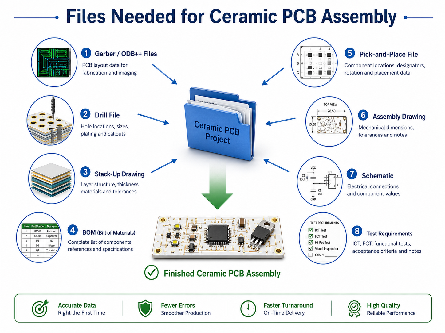
For quick turn DPC ceramic PCB fabrication, design files should be reviewed before ordering. A fast quote is helpful, but a fast technical review is more important.
Recommended design checks:
- Keep enough distance from copper to board edge.
- Avoid sharp inside corners in copper patterns.
- Use rounded corners where stress may concentrate.
- Confirm minimum line width and spacing with the factory.
- Avoid unnecessary large copper imbalance.
- Check pad size for soldering, wire bonding, or die attach.
- Define plated and non-plated holes clearly.
- Mark ceramic material and thickness in the drawing.
- Add surface finish and tolerance requirements.
- Confirm assembly temperature and soldering process.
For bare substrate projects, include Gerber, drill files, outline drawing, material requirement, copper thickness, surface finish, tolerance notes, and inspection requirements. For assembled projects, also include BOM, pick-and-place file, polarity drawing, solder paste layer, and test requirements.
Manufacturing Considerations for Fast Delivery
Quick turn ceramic PCB production depends on design complexity. A simple single-sided or double-sided DPC ceramic PCB can move faster than a complex board with tight spacing, many laser holes, special surface finish, thick copper, or strict cosmetic standards.
To improve lead time, buyers should provide:
- Complete fabrication files
- Clear material requirement
- Quantity and panelization preference
- Copper thickness
- Surface finish
- Tolerance drawing
- Final application notes
- Required test standard
- Packaging requirement
- Target delivery date
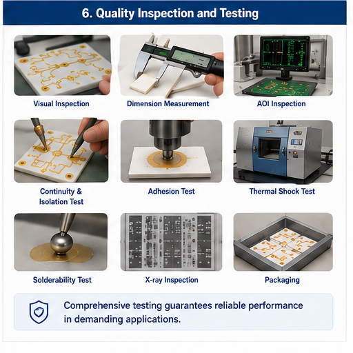
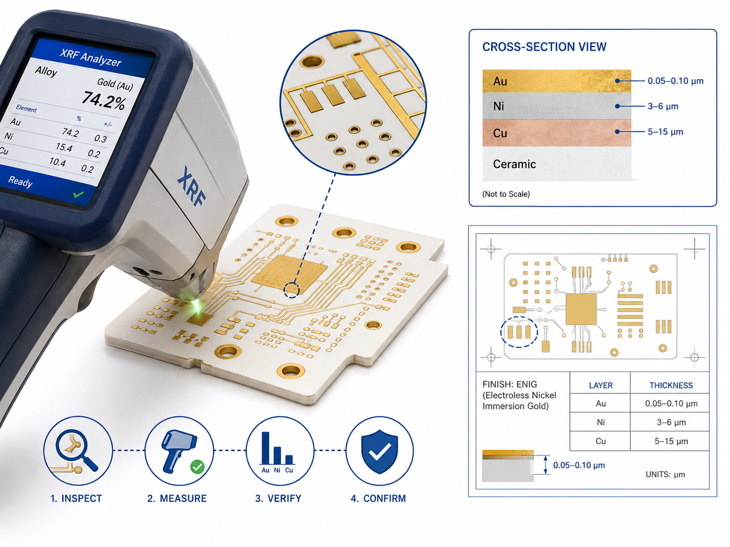
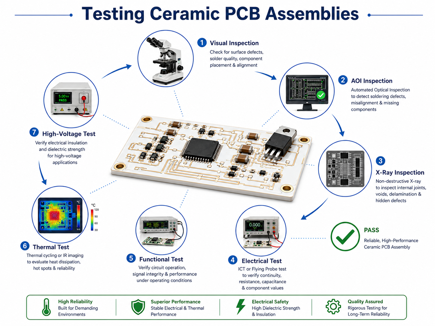
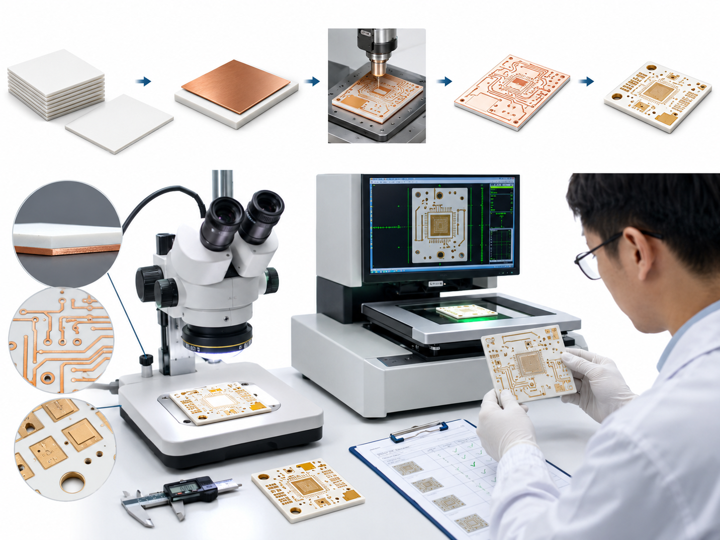
Fast delivery does not mean skipping inspection. A reliable manufacturer should still run incoming ceramic inspection, dimensional check, copper thickness measurement, surface finish inspection, AOI, electrical testing, and final visual inspection.
IPC standards are commonly used to align quality expectations in electronics manufacturing. IPC standards help define reliability, quality, and consistency across the electronics industry, while IPC-A-600 is widely used as a visual acceptability reference for printed boards.
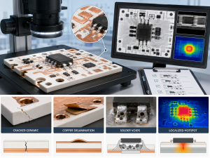
Common Failure Modes in DPC Ceramic PCB
DPC ceramic PCB failures usually come from material mismatch, process instability, poor handling, or design stress.
Common failure modes include:
| Failure Mode | Possible Cause | Prevention |
|---|---|---|
| Copper peeling | Weak adhesion or poor surface preparation | Adhesion test and process control |
| Ceramic cracking | Mechanical stress or poor mounting | Review hole position, edge clearance, fixture pressure |
| Open circuit | Etching or plating defect | AOI and electrical test |
| Short circuit | Insufficient spacing or contamination | DFM review and ionic cleanliness control |
| Solder voiding | Poor pad design or reflow control | Optimize stencil, finish, and profile |
| Warpage issue | Uneven copper or thermal stress | Balanced copper and controlled firing/plating process |
| Poor bonding | Surface finish mismatch | Confirm wire bonding or die attach requirement early |
| Thermal failure | Wrong material or insufficient copper area | Thermal simulation and material upgrade |
A practical failure analysis should not stop at “bad board.” It should check the full chain: substrate, copper adhesion, finish, soldering, fixture, thermal interface, device power, operating environment, and handling process.
What Affects DPC Ceramic PCB Cost?
The cost of DPC ceramic PCB fabrication depends on material, copper thickness, circuit density, tolerance, surface finish, inspection level, and delivery speed.
Main cost factors include:
- Ceramic material: AlN costs more than common alumina.
- Board thickness: Special thickness may require custom sourcing.
- Copper thickness: More plating time increases cost.
- Line width and spacing: Fine features require tighter process control.
- Hole processing: Laser drilling adds cost.
- Surface finish: ENIG and special finishes cost more than basic options.
- Quantity: Prototype unit price is higher than batch price.
- Testing: Extra reliability tests increase cost.
- Lead time: Urgent production may need priority scheduling.
- Packaging: Fragile ceramic boards need careful protection.
The best cost-control method is not choosing the cheapest material. It is matching the material to the real thermal, electrical, and mechanical requirement. Over-specification wastes budget. Under-specification creates redesign cost.
How to Ensure Quality in DPC Ceramic PCB Fabrication?
Quality control should start before production. For ceramic PCB, small design errors can become expensive after plating, finishing, or assembly.
Recommended quality controls include:
- DFM review before production
- Ceramic substrate inspection
- Copper thickness measurement
- Adhesion test
- Line width and spacing inspection
- Hole size and position inspection
- Surface finish thickness check
- AOI
- Electrical test
- Insulation resistance test
- Solderability test when required
- Final visual inspection
- Moisture-proof and shock-resistant packaging
For high-reliability applications, buyers may also request cross-section analysis, thermal cycling, pull test, shear test, ionic contamination test, and traceability documentation.
A good quick turn supplier should not only say “we can make it fast.” The supplier should explain what can be accelerated, what cannot be shortened, and which specifications may affect risk.
How to Choose a DPC Ceramic PCB Supplier?
A suitable DPC ceramic PCB supplier should understand both ceramic substrate processing and electronic manufacturing requirements.
Use the following supplier checklist:
- Can the factory support DPC ceramic PCB fabrication directly?
- Does the team understand alumina and AlN material selection?
- Can they review line width, spacing, copper thickness, and hole design?
- Can they support quick turn prototype and batch production?
- Do they provide DFM feedback before production?
- Can they perform AOI, e-test, copper thickness inspection, and surface finish checks?
- Can they support RoHS-compliant materials and documentation?
- Do they have experience with LED, power, RF, medical, automotive, or industrial projects?
- Can they package ceramic boards safely for international shipping?
- Can they support custom OEM and ODM engineering projects?
For buyers sourcing from China, the best approach is to choose a real manufacturing partner with technical review capability, not only a trading quotation channel. Cross-border purchasing can work very well when files are complete, requirements are clear, and the factory has stable process control.
What Should Buyers Check Before Placing an Order?
Before ordering, confirm the information below:
- Final application
- Ceramic material
- Board size
- Thickness
- Copper thickness
- Layer structure
- Line width and spacing
- Hole type and size
- Surface finish
- Solder mask requirement
- Quantity
- Delivery requirement
- Inspection standard
- Assembly requirement
- Packaging method
- Shipping destination
- Compliance requirement
For quick turn orders, avoid vague instructions such as “standard ceramic PCB” or “same as normal PCB.” DPC ceramic PCB fabrication needs precise material and process details.
A strong RFQ package reduces delays, prevents incorrect assumptions, and helps the manufacturer give a more accurate price.
FAQ About Quick Turn DPC Ceramic PCB Fabrication
What does DPC mean in ceramic PCB manufacturing?
DPC means Direct Plated Copper or Direct Plating Copper. It is a ceramic PCB process where a metal seed layer is formed on the ceramic surface, then copper is built up by electroplating. It is often used for fine circuits, compact pads, thermal substrates, and high-power electronic modules.
Is DPC ceramic PCB better than FR4 PCB?
DPC ceramic PCB is better when the project needs high thermal conductivity, electrical insulation, and stable performance under heat. FR4 is still better for many low-cost signal boards. The right choice depends on heat density, voltage, product lifetime, assembly method, and total project budget.
Is DPC better than DBC ceramic substrate?
DPC is usually better for fine circuit patterns, smaller pads, and prototype validation. DBC is often better for thick copper and high-current power modules. If the project needs fine routing and good surface flatness, DPC may be preferred. If it needs heavy copper current capacity, DBC may fit better.
Can DPC ceramic PCB be made quickly?
Yes, simple DPC ceramic PCB prototypes can often be produced with quick turn scheduling. Lead time depends on material availability, copper thickness, circuit density, hole processing, surface finish, testing, and order quantity. Complete files and clear specifications help reduce engineering delays before production starts.
Which material is better, alumina or aluminum nitride?
Alumina is more cost-effective and works well for many LED, sensor, and industrial electronics projects. Aluminum nitride provides much better heat dissipation and is suitable for high-power LEDs, laser modules, power devices, and compact thermal designs. The selection should follow thermal load and budget.
Can DPC ceramic PCB support fine lines?
Yes, DPC is suitable for fine circuit patterns because copper is plated and patterned with a precision process. However, actual minimum line width and spacing depend on the factory’s capability, copper thickness, ceramic size, and yield requirement. Always confirm the capability before final layout.
What files are needed for a DPC ceramic PCB quote?
A complete quote package should include Gerber files, drill files, board outline, ceramic material, substrate thickness, copper thickness, surface finish, quantity, tolerance notes, and application details. For assembly, also provide BOM, pick-and-place file, polarity drawing, test method, and soldering requirement.
Why does DPC ceramic PCB cost more than FR4?
DPC ceramic PCB costs more because ceramic material, surface preparation, thin-film metallization, copper plating, precision etching, and inspection are more specialized than standard FR4 production. The higher cost is usually justified when heat dissipation, insulation, or compact power density affects product reliability.
Can DPC ceramic PCB be used for high-power LED modules?
Yes, high-power LED modules are one of the common applications. DPC ceramic PCB can help transfer heat from the LED pad to the ceramic substrate and heatsink. For best results, engineers should also control solder voids, pad design, mounting pressure, and thermal interface material.
What causes copper peeling on DPC ceramic PCB?
Copper peeling may come from weak surface activation, poor seed-layer adhesion, plating issues, contamination, thermal stress, or unsuitable assembly conditions. Prevention requires proper ceramic cleaning, stable metallization, adhesion testing, controlled plating, compatible surface finish, and correct soldering or bonding process.
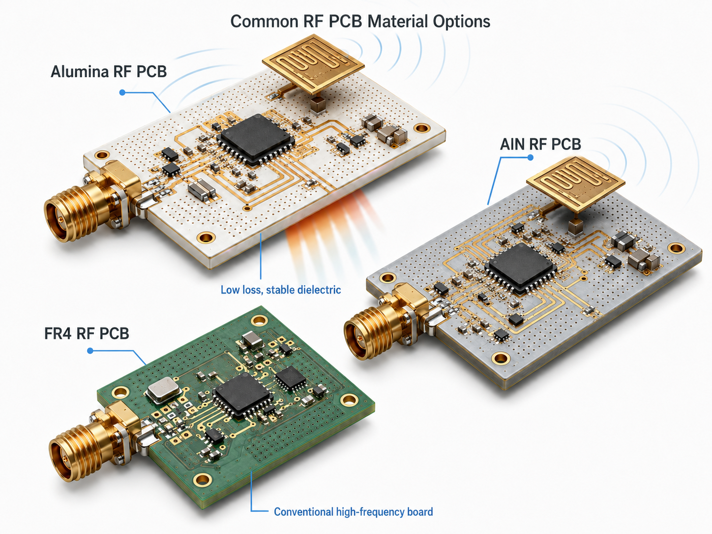
Can DPC ceramic PCB be used for RF applications?
DPC ceramic PCB can be used in some RF and microwave-related modules when the material, dielectric properties, line geometry, surface finish, and grounding design are suitable. For RF designs, engineers should confirm dielectric constant, loss, copper roughness, impedance requirement, and frequency range before fabrication.
Is DPC ceramic PCB suitable for automotive electronics?
Yes, it can be suitable for automotive lighting, power modules, sensors, and thermal management circuits. Automotive projects should pay close attention to thermal cycling, vibration, insulation, material traceability, process documentation, and long-term reliability validation before moving from prototype to mass production.
How can buyers reduce risk when ordering from a China factory?
Buyers should provide complete files, request DFM review, confirm material and copper thickness, define inspection requirements, check compliance documentation, and start with prototypes before mass production. A real source factory with engineering support can reduce communication gaps and improve repeatability for global delivery.
What is the most common design mistake in DPC ceramic PCB?
A common mistake is treating ceramic PCB like ordinary FR4. Ceramic is rigid and brittle, so edge distance, mounting pressure, hole position, copper balance, soldering method, and thermal interface design all matter. Early DFM review helps prevent cracks, peeling, poor soldering, and thermal failures.
When should a project move from prototype to batch production?
Move to batch production after confirming electrical performance, thermal behavior, solderability, surface finish, dimensional fit, adhesion, and reliability under real operating conditions. For high-power or regulated applications, it is better to validate a small pilot batch before releasing full-volume production.
Conclusion:
Quick turn DPC ceramic PCB fabrication is most valuable when a project needs fast prototype validation, strong heat dissipation, compact routing, reliable insulation, and a clear path toward batch production. The core technical point is that DPC ceramic PCB should be designed as part of the thermal and electrical system, not only as a circuit carrier.
If you need quick turn DPC ceramic PCB fabrication, ceramic PCB prototypes, OEM manufacturing, ODM production, small-batch trial production, or custom engineering support, you are welcome to contact our engineering team for technical review and quotation service. Send your Gerber files, drawings, stack-up, material requirements, and quantity to sales@bestpcbs.com, and our team will help evaluate the most suitable manufacturing solution for your project.