Low thermal expansion metals are used in electronics packaging and ceramic substrates to reduce stress caused by temperature changes. In a package, materials such as semiconductor chips, ceramic substrates, copper layers, solder joints, metal frames, and base plates expand at different rates. If this expansion mismatch is too large, it may lead to warpage, cracking, delamination, solder fatigue, or sealing failure.
This is why low CTE metals and controlled expansion alloys are commonly used in power modules, laser packages, RF devices, sensors, ceramic-to-metal structures, and other high-reliability electronic assemblies. This guide explains what low thermal expansion metals are, why they matter in electronic packaging, how they work with ceramic substrates, and how to choose the right material for engineering projects.
What Are Low Thermal Expansion Metals?
Low thermal expansion metals are metals or metal alloys that change very little in size when temperature changes. Their expansion rate is measured by the coefficient of thermal expansion, usually called CTE.
A low CTE material expands less than a high CTE material under the same temperature rise. This is useful when different materials are bonded together and must stay stable during heating and cooling.
In electronics packaging, low thermal expansion metals are selected for several reasons:
- Better dimensional stability
- Lower stress between bonded materials
- Better CTE matching with ceramic or semiconductor materials
- Improved thermal cycling reliability
- Support for hermetic sealing
- Compatibility with brazing, soldering, plating, or metallization
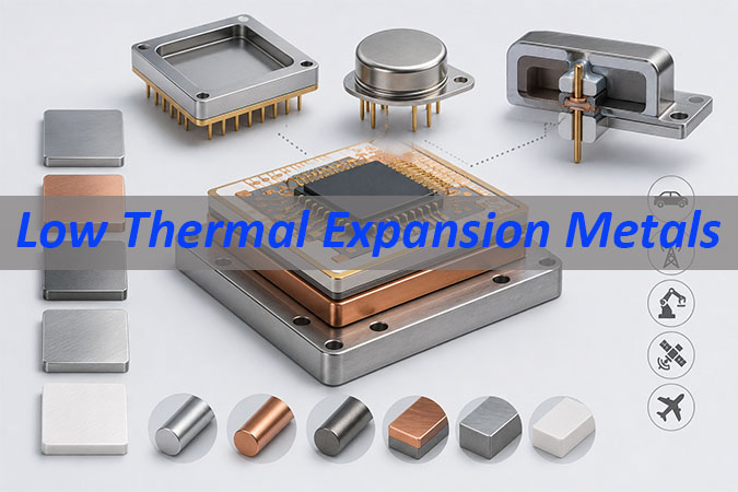
Common low thermal expansion metals include:
- Invar
- Kovar
- Alloy 42
- Molybdenum
- Tungsten
- Copper tungsten
- Copper molybdenum
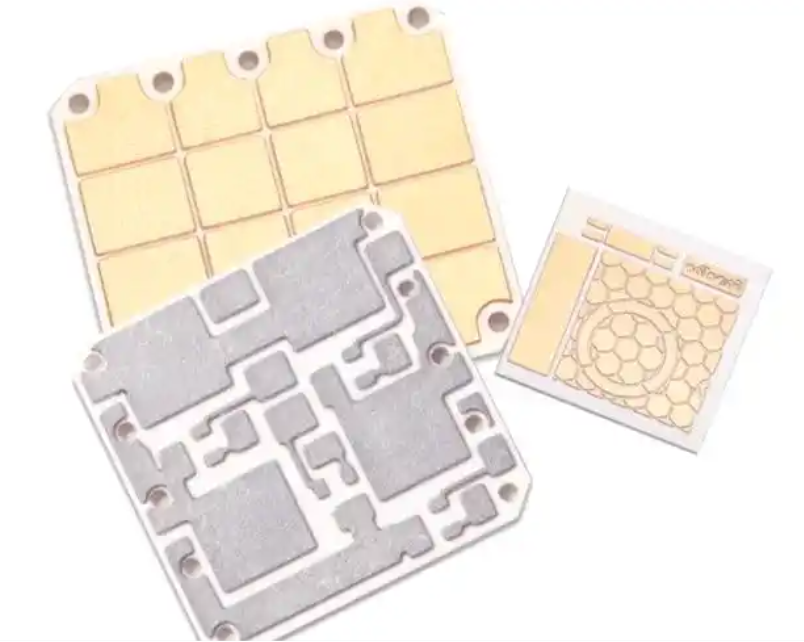
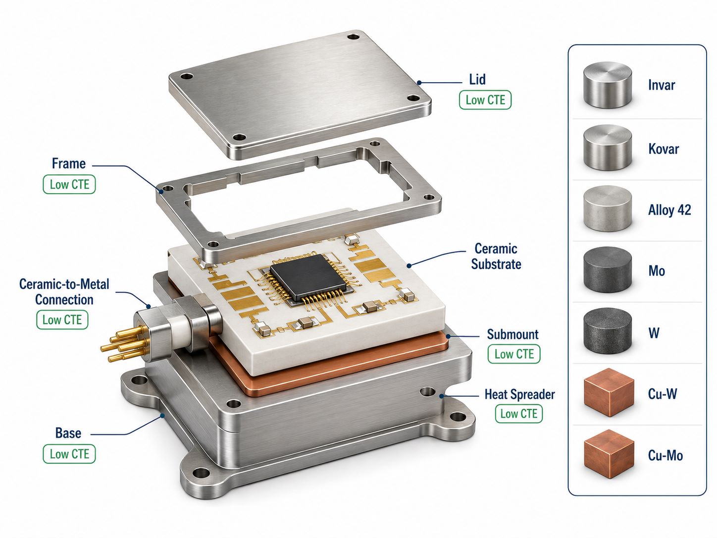
For ceramic substrate projects, these metals are usually not used as the circuit carrier. Instead, they are often used as:
- Frames
- Lids
- Bases
- Carriers
- Inserts
- Heat spreaders
- Submounts
- Ceramic-to-metal connection parts
Why Is Thermal Expansion Important in Electronics Packaging?
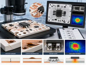
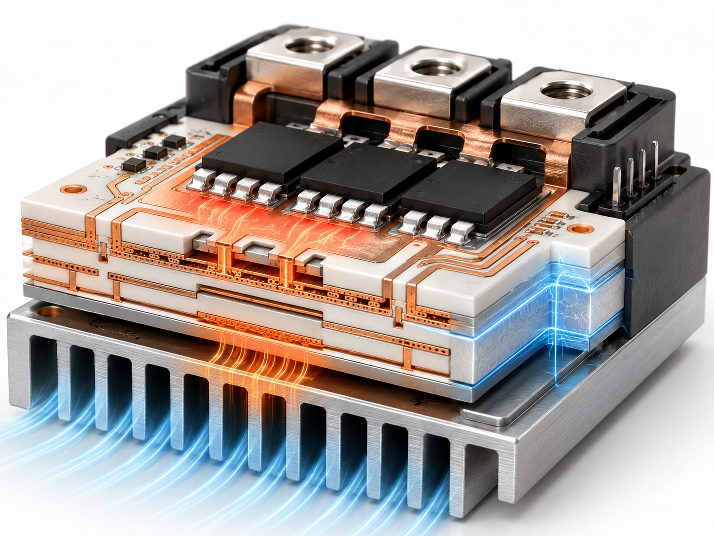
Thermal expansion becomes important when several materials are bonded in one package. A typical electronic package may include silicon, ceramic, copper, solder, metal plating, epoxy, and a metal housing. Each material has a different expansion rate.
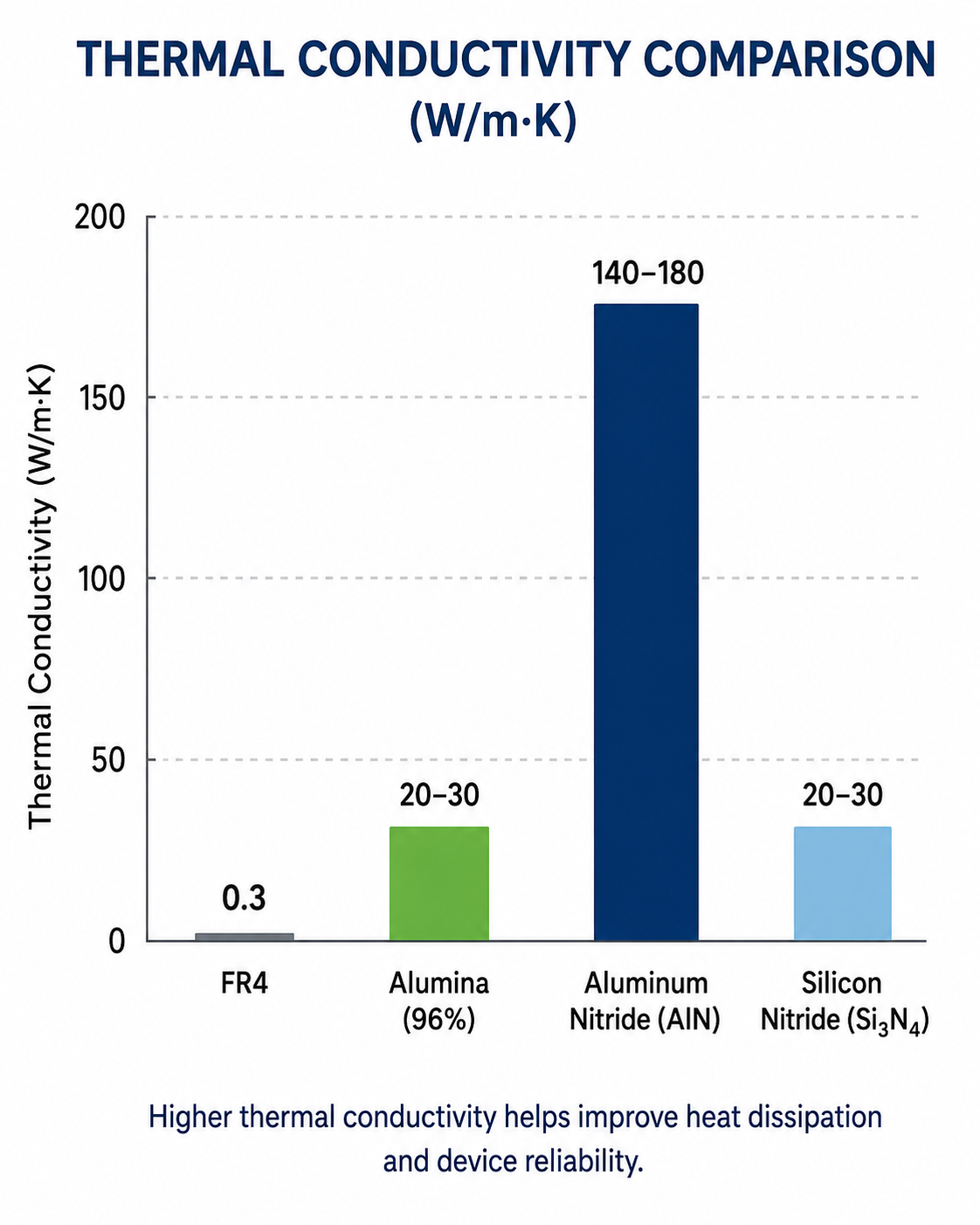
Silicon has a low CTE. Ceramic materials such as aluminum nitride, alumina, and silicon nitride also expand less than copper or aluminum. Copper is excellent for electrical and thermal conduction, but it expands much more than many ceramic and semiconductor materials.
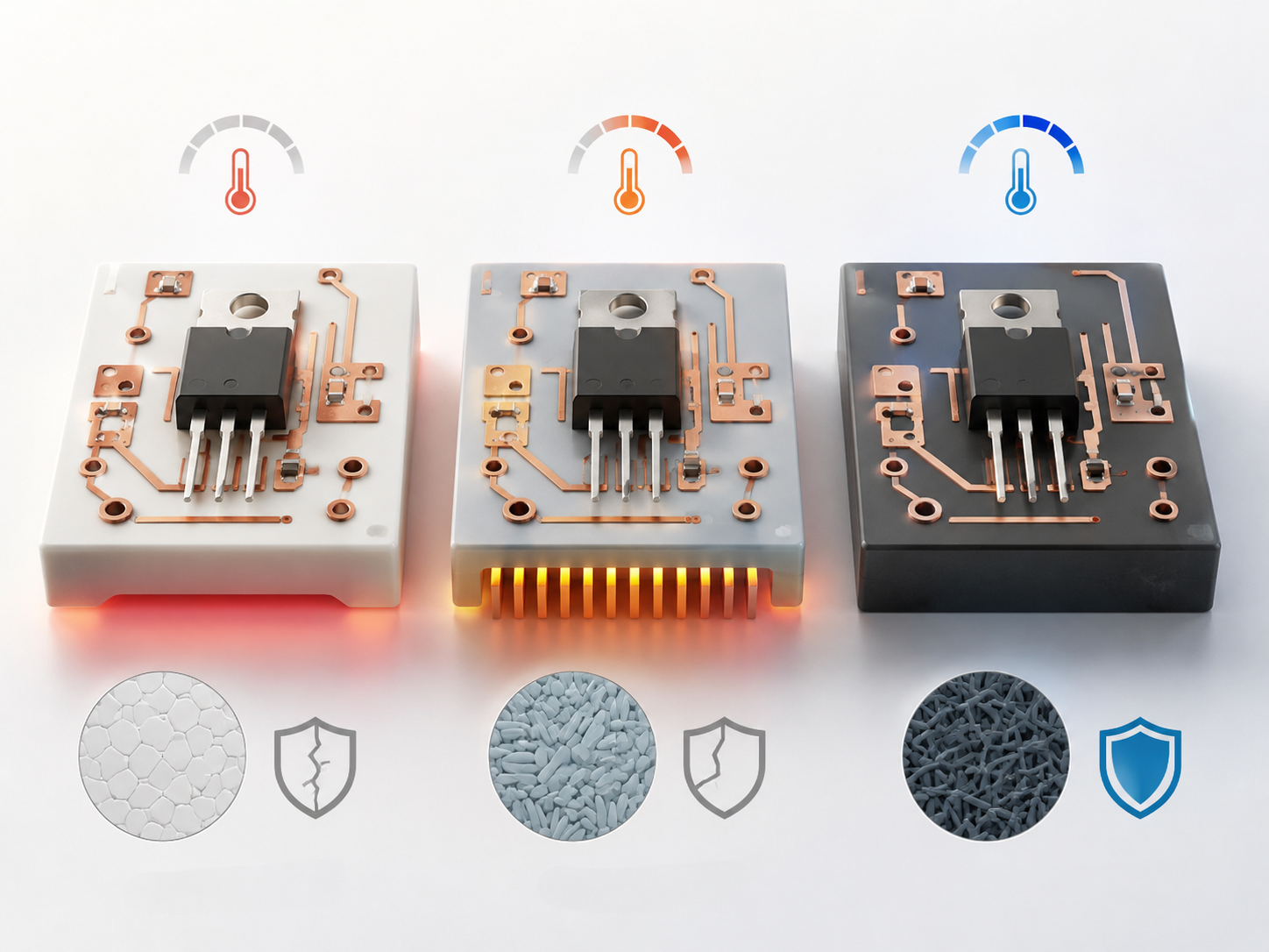
When the package heats and cools, each layer tries to move at its own rate. Because the layers are bonded together, this movement creates internal stress.
Thermal expansion mismatch may cause:
- Ceramic cracks
- Copper layer delamination
- Solder joint fatigue
- Package warpage
- Seal leakage
- Shorter thermal cycling life
- Stress on chips, wire bonds, or die attach layers
For high-power electronics, RF modules, aerospace electronics, optoelectronic packages, and ceramic packaging, CTE matching is a key part of reliability design. Good thermal design is not only about moving heat away. It is also about keeping the structure mechanically stable while heat moves through it.
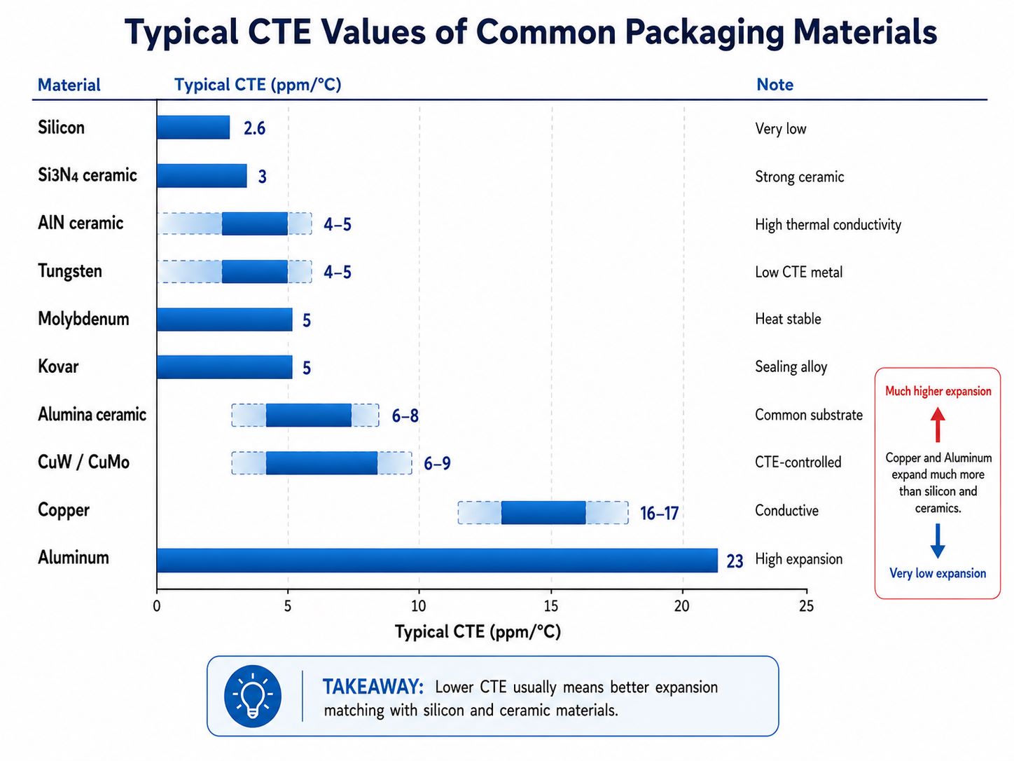
What Is the Coefficient of Thermal Expansion in Metals?
The coefficient of thermal expansion shows how much a material expands when temperature rises. It is usually expressed in ppm/°C or µm/m·°C.
For example, a CTE of 5 ppm/°C means one meter of material expands about 5 micrometers for every 1°C increase.
Typical values vary by grade, temperature range, and processing method. Still, the table below gives a useful engineering reference.
| Material | Typical CTE | Note |
|---|---|---|
| Silicon | ~2.6 ppm/°C | Very low |
| Si₃N₄ ceramic | ~3 ppm/°C | Strong ceramic |
| AlN ceramic | ~4–5 ppm/°C | High thermal conductivity |
| Tungsten | ~4–5 ppm/°C | Low CTE metal |
| Molybdenum | ~5 ppm/°C | Heat stable |
| Kovar | ~5 ppm/°C | Sealing alloy |
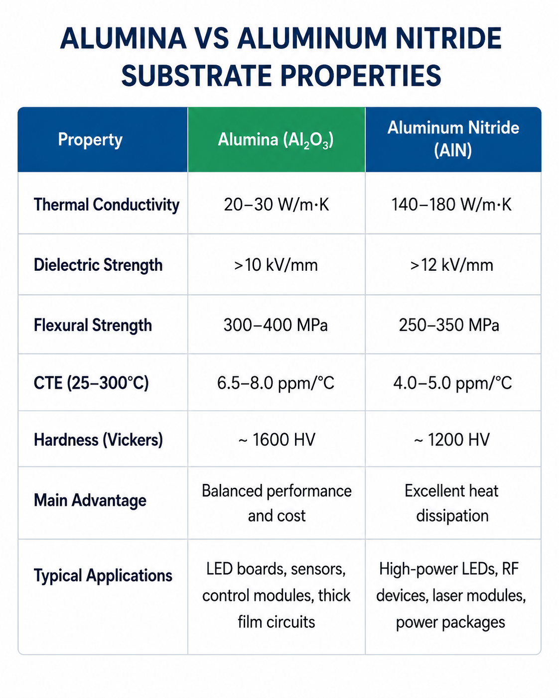
| Alumina ceramic | ~6–8 ppm/°C | Common substrate |
| CuW / CuMo | ~6–9 ppm/°C | CTE-controlled |
| Copper | ~16–17 ppm/°C | Conductive |
| Aluminum | ~23 ppm/°C | High expansion |
This is why material matching matters. Copper conducts heat very well, but its CTE is much higher than silicon, AlN, or Si₃N₄. If copper is bonded to ceramic in a high-stress structure, the design must control that mismatch.
Low coefficient of thermal expansion metals help reduce the expansion gap. They cannot remove all stress, but they can make the package more stable and predictable.
What Metals Have Low Thermal Expansion?
Metals with low thermal expansion can be grouped into three main types.
| Type | Examples | Main Use |
|---|---|---|
| Controlled expansion alloys | Invar, Kovar, Alloy 42 | Frames, lids, seals |
| Refractory metals | Tungsten, molybdenum | High-temperature parts |
| CTE-controlled composites | CuW, CuMo | Bases, heat spreaders |
Main material groups include:
- Controlled expansion alloys
These alloys are designed to keep expansion low or close to specific glass, ceramic, or semiconductor materials. Invar, Kovar, and Alloy 42 are common examples. - Refractory metals
These metals have low CTE and strong high-temperature stability. Tungsten and molybdenum are widely used in demanding electronic, vacuum, and high-temperature structures. - CTE-controlled composite metals
These materials combine low expansion and better heat transfer. Copper tungsten and copper molybdenum are often selected for semiconductor package bases, RF packages, laser modules, and power device structures.
Common Low Thermal Expansion Metals and Alloys
Different low thermal expansion metals serve different purposes. A low CTE number alone is not enough. Engineers also need to consider:
- Thermal conductivity
- Mechanical strength
- Machinability
- Plating compatibility
- Brazing or soldering method
- Cost
- Working temperature
- Matched ceramic or semiconductor material
Invar
- Iron-nickel alloy with very low expansion near room temperature
- Suitable for precision structures, optical systems, measuring devices, and stable mechanical frames
- Can be used for support parts or frame structures in electronic packaging
- Not the best option when strong heat spreading is required
Kovar
- Controlled expansion alloy used in glass-to-metal and ceramic-to-metal sealing
- Expansion behavior is close to many sealing materials
- Helps reduce stress around hermetic seals
- Commonly used for lids, frames, leads, headers, feedthroughs, and hermetic housings
Alloy 42
- Iron-nickel alloy with controlled expansion
- Used in electronic packages and lead frames
- Provides stable expansion and good manufacturability
- Suitable when the design needs controlled expansion but not the extremely low CTE of Invar
Molybdenum
- Low CTE metal with good thermal stability
- More thermally conductive than many low expansion alloys
- Used in high-temperature supports, metallization systems, and specialized package components
- Suitable for ceramic-related structures that need stability under heat
Tungsten
- Very low expansion and excellent high-temperature resistance
- Dense and harder to process than many common metals
- Suitable for applications where stability and heat resistance are critical
- Often used in demanding electronic, vacuum, or high-temperature structures
Copper Tungsten
- Combines tungsten’s low expansion with copper’s thermal conductivity
- CTE and thermal performance can be adjusted by changing the copper-tungsten ratio
- Common in semiconductor bases, RF packages, power devices, and heat spreaders
- Useful near ceramic substrates when both heat transfer and CTE control are required
Copper Molybdenum
- Balances expansion control and thermal conductivity
- Used as a base plate, submount, or heat spreader
- Suitable for packages that require CTE matching and heat transfer
- Often considered for ceramic packaging and power electronics structures
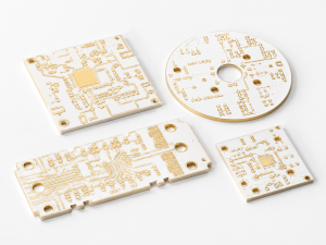
How Do Low Thermal Expansion Metals Work with Ceramic Substrates?
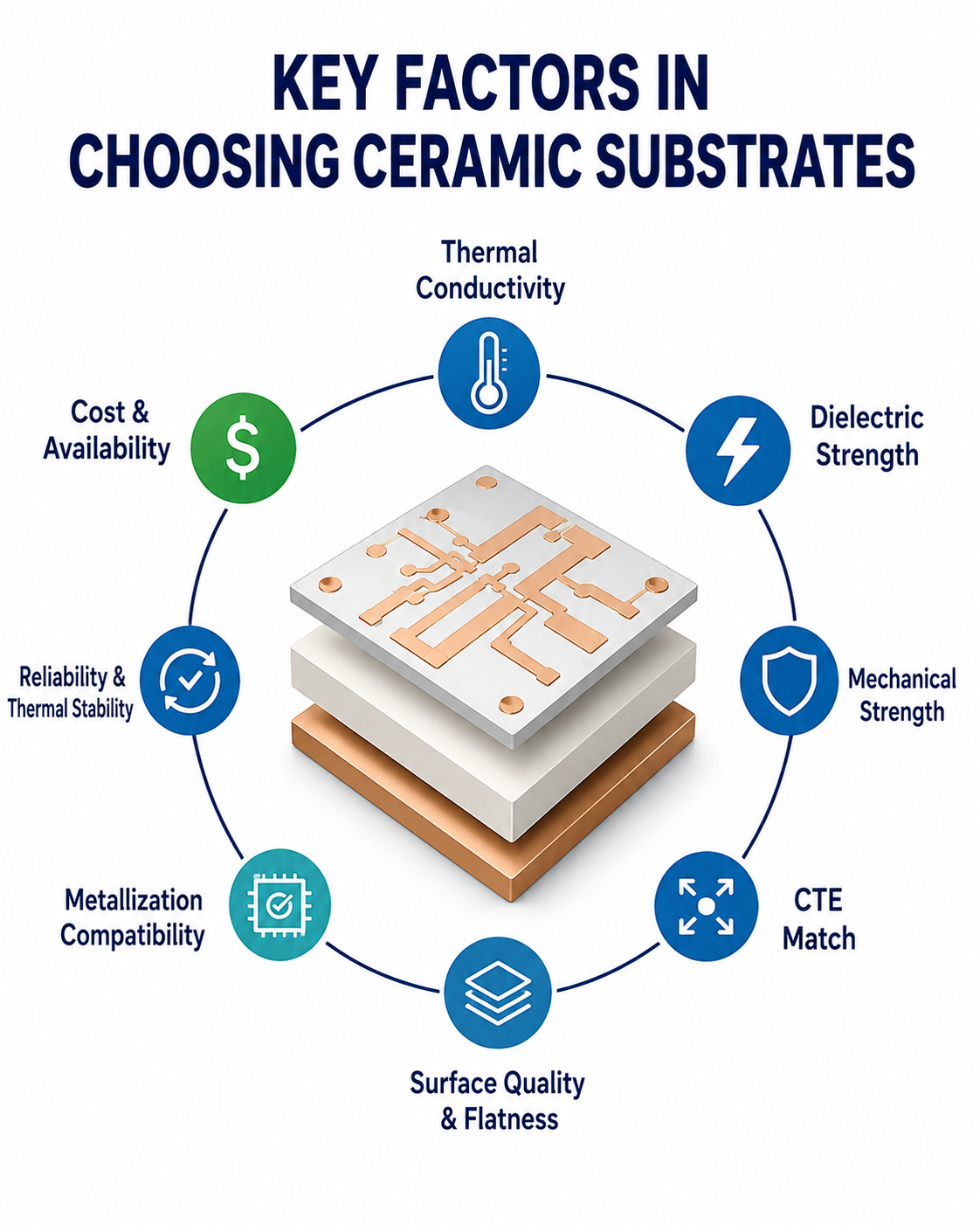
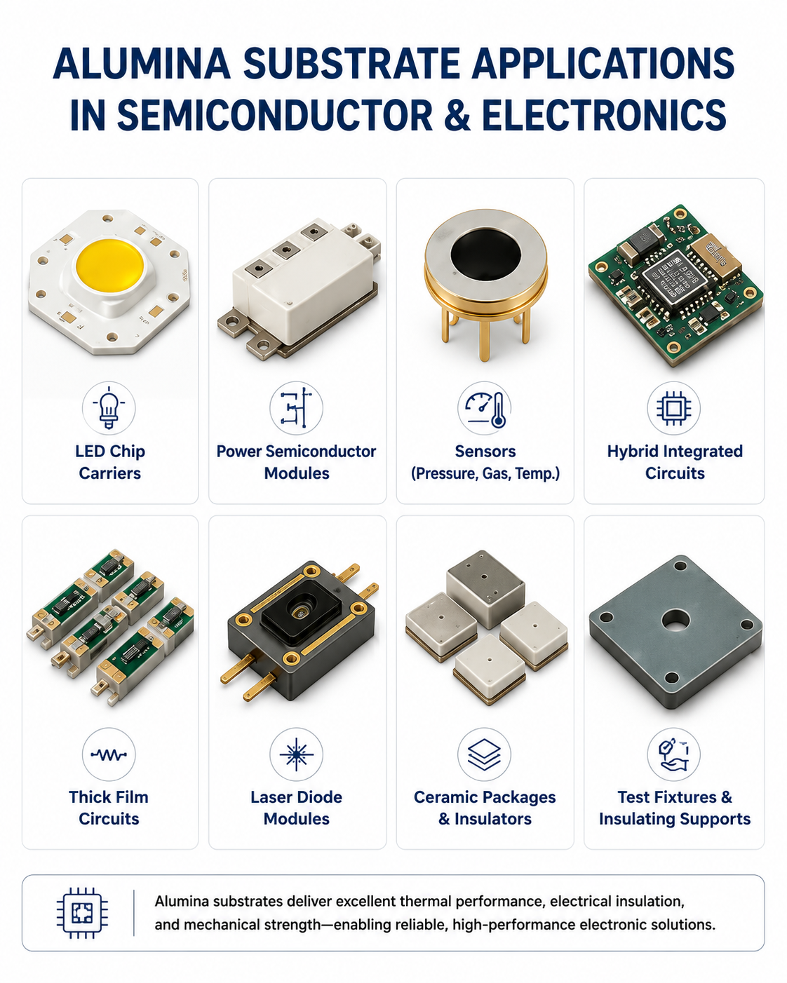
Ceramic substrates such as alumina, aluminum nitride, and silicon nitride are used in high-power and high-reliability electronics because they provide:
- Electrical insulation
- Thermal stability
- Heat resistance
- Good dimensional stability
- Better performance than many polymer-based PCB materials in harsh environments
However, ceramics are brittle compared with metals. They can handle high temperatures, but they do not tolerate excessive tensile stress well. If a metal part expands much more than the ceramic, stress may concentrate at the bonding interface or ceramic edge.
Low thermal expansion metals help reduce this expansion difference.
They may be used as:
- Package bases under ceramic substrates
- Metal frames around ceramic packages
- Heat spreaders between chips and substrates
- Ceramic-to-metal sealing parts
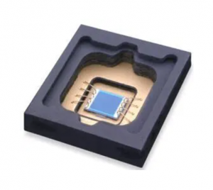
- Submounts for laser diodes or power semiconductors
- Controlled expansion inserts
- Metal lids or housings for hermetic packages
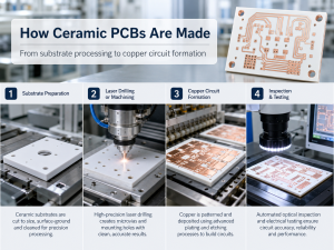
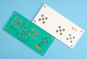
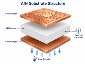
In a ceramic PCB or ceramic substrate project:
- The ceramic substrate provides insulation and circuit support.
- The metal layer provides electrical or thermal conduction.
- The low CTE metal helps improve mechanical stability.
- The joining layer must survive thermal cycling.
- The full material stack must be reviewed together.
This distinction is important. Low thermal expansion metals do not replace ceramic substrates. They support the ceramic substrate inside a more reliable package.
Low Thermal Expansion Metals vs Ceramic Substrate Materials
Low expansion metals and ceramic substrates may both have low CTE values, but they have different functions.
| Item | Low Expansion Metals | Ceramic Substrates |
|---|---|---|
| Main role | Support, CTE control | Circuit carrier, insulation |
| Examples | Kovar, Invar, CuW, CuMo | Al₂O₃, AlN, Si₃N₄ |
| Electrical property | Conductive | Insulating |
| Thermal role | Spread heat or reduce stress | Transfer heat with insulation |
| Mechanical behavior | Tougher | Hard but brittle |
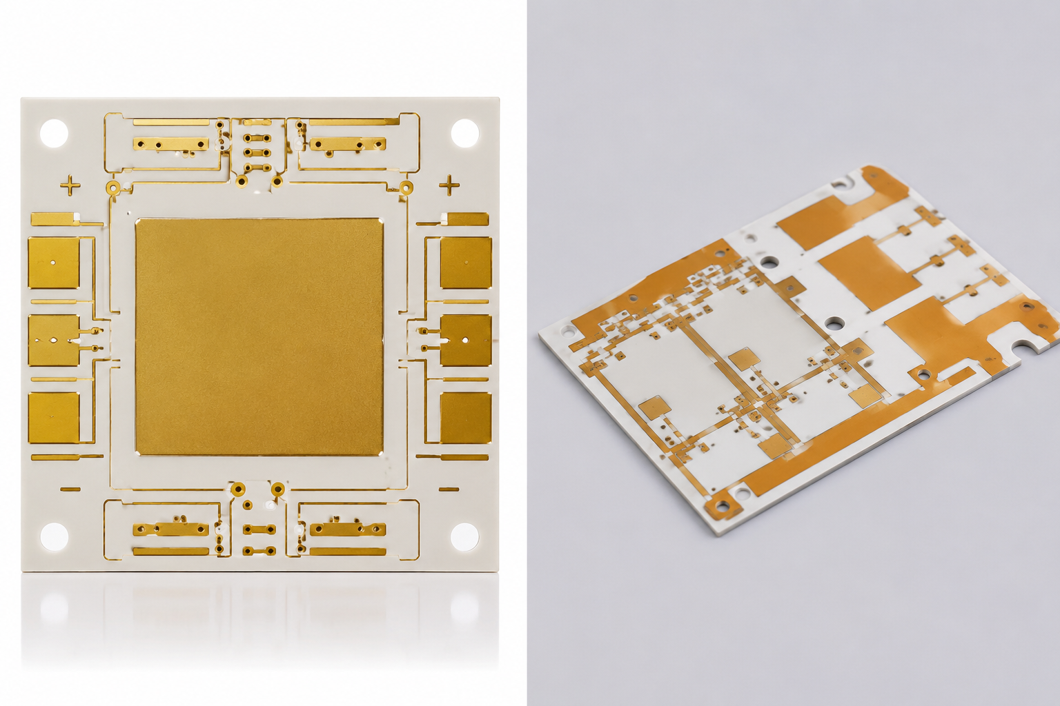
| Common use | Frame, base, lid | DBC, DPC, AMB, ceramic PCB |
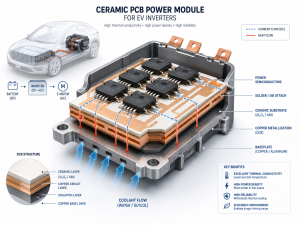
For power electronics, AlN and Si₃N₄ substrates are often selected for thermal and mechanical performance. But the full package may still need metal parts with suitable expansion behavior.
For example:
- A ceramic substrate carries the circuit and provides insulation.
- A CuW or CuMo base helps reduce stress and spread heat.
- A Kovar frame supports hermetic sealing.
- A molybdenum part improves stability in high-temperature structures.
The best design usually comes from matching the full material stack, not choosing one material alone.
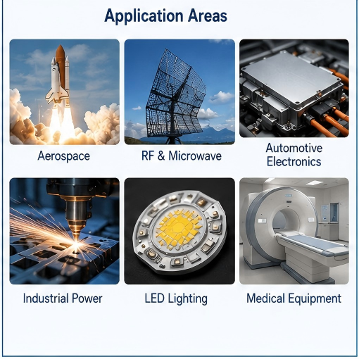
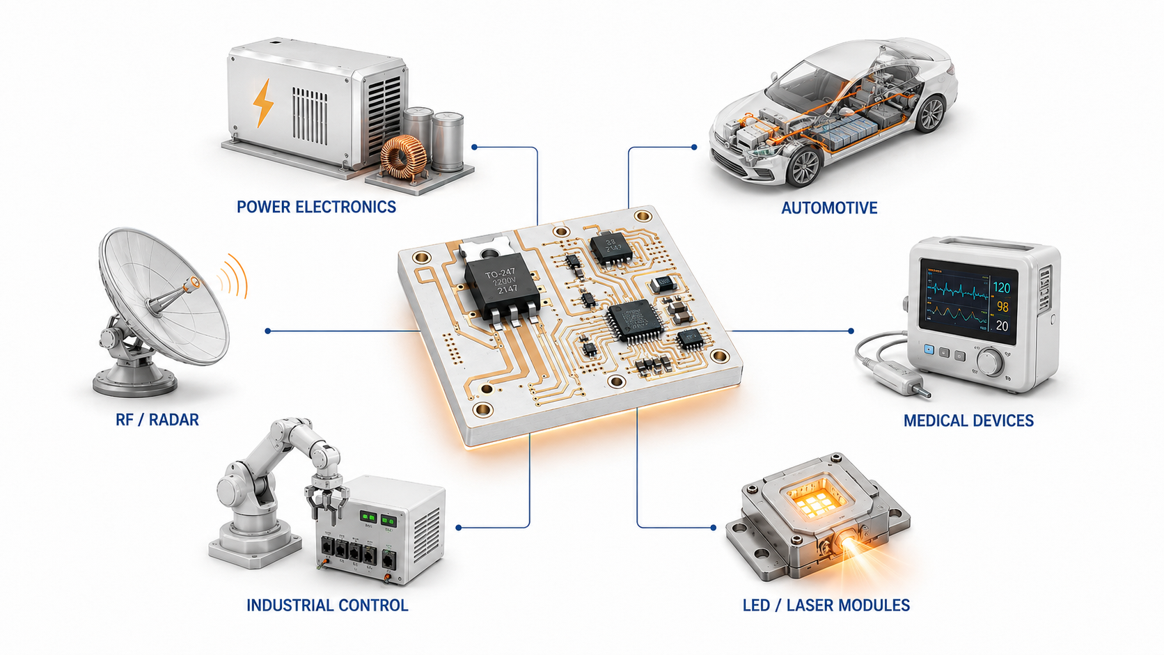
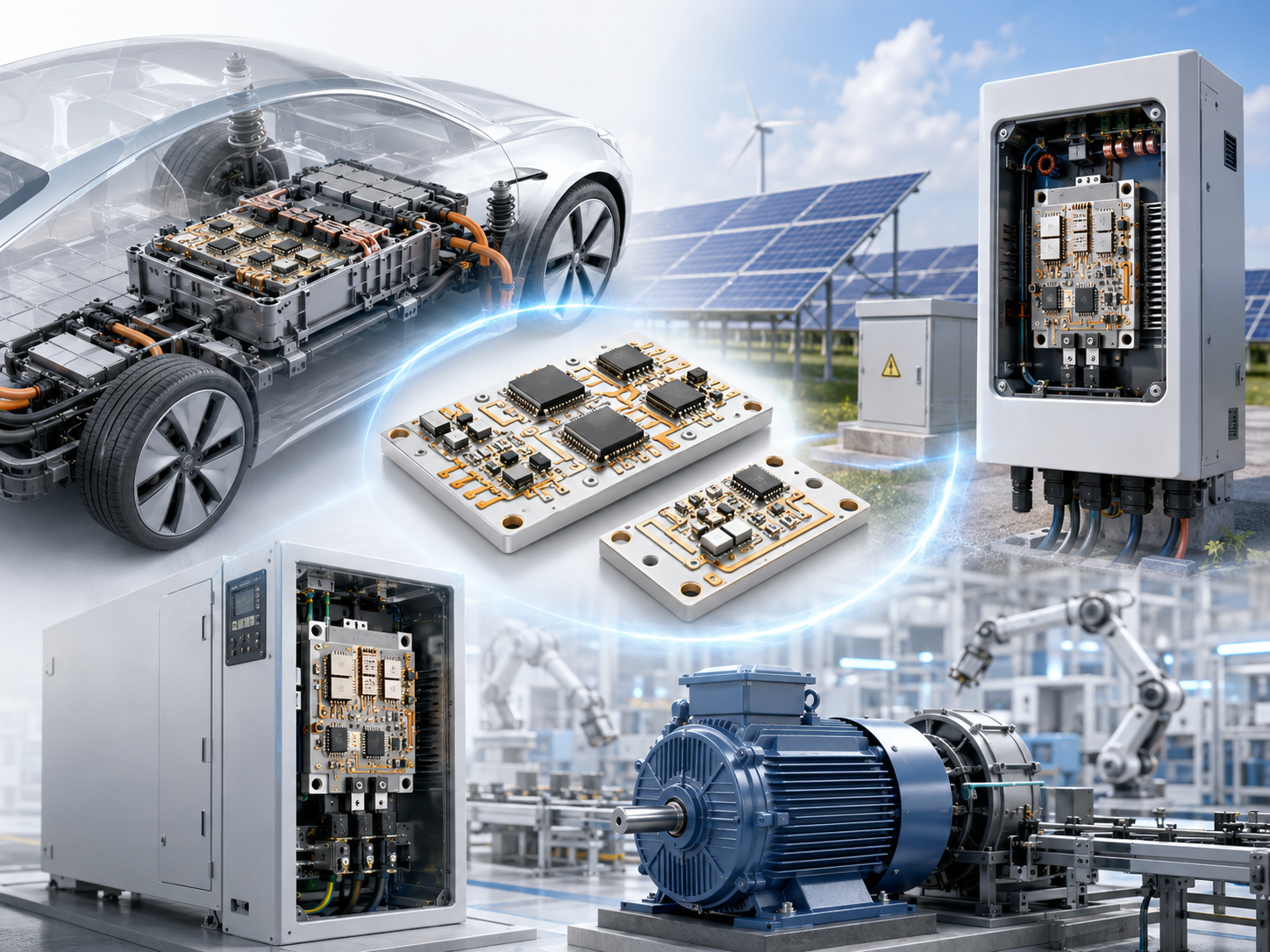
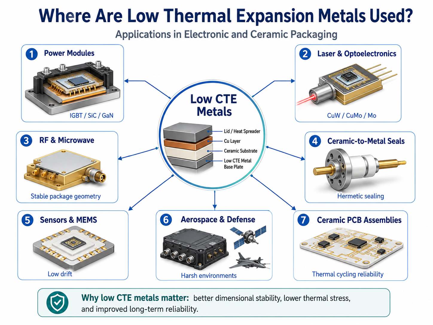
Where Are Low Thermal Expansion Metals Used in Electronic and Ceramic Packaging?
Low thermal expansion metals are used where thermal cycling, precision, sealing, and material compatibility matter. Their value is often hidden inside the package, but it affects long-term reliability.
- Power semiconductor modules
Power modules based on IGBT, MOSFET, SiC, or GaN devices generate heat during operation. The package may include ceramic substrates, copper layers, solder, base plates, and semiconductor chips. Low CTE metals or composites help reduce stress in the stack. - Laser diode and optoelectronic packages
Laser diodes are sensitive to alignment and thermal drift. A small dimensional change may affect optical performance. CuW, CuMo, Kovar, and molybdenum may be used in submounts, bases, and housings. - RF and microwave packages
RF packages often need stable dimensions, controlled grounding, and reliable sealing. Kovar, CuW, and related materials are used for frames, bases, lids, and package housings. - Ceramic-to-metal seals
Ceramic-to-metal seals are used in feedthroughs, vacuum devices, sensors, aerospace electronics, medical electronics, and high-reliability connectors. Kovar is often selected for these sealing structures. - Sensors and MEMS packaging
Sensor packages may require mechanical stability and low drift. Low expansion materials help keep package geometry stable during temperature changes. - Aerospace and defense electronics
Aerospace electronics may face wide temperature ranges, vibration, and long service life requirements. Low thermal expansion metals help improve package integrity in harsh conditions. - High-reliability ceramic PCB assemblies
In ceramic PCB projects, low CTE metals may be used in fixtures, frames, bases, or thermal spreaders. They help the ceramic substrate work reliably under thermal shock or power cycling.
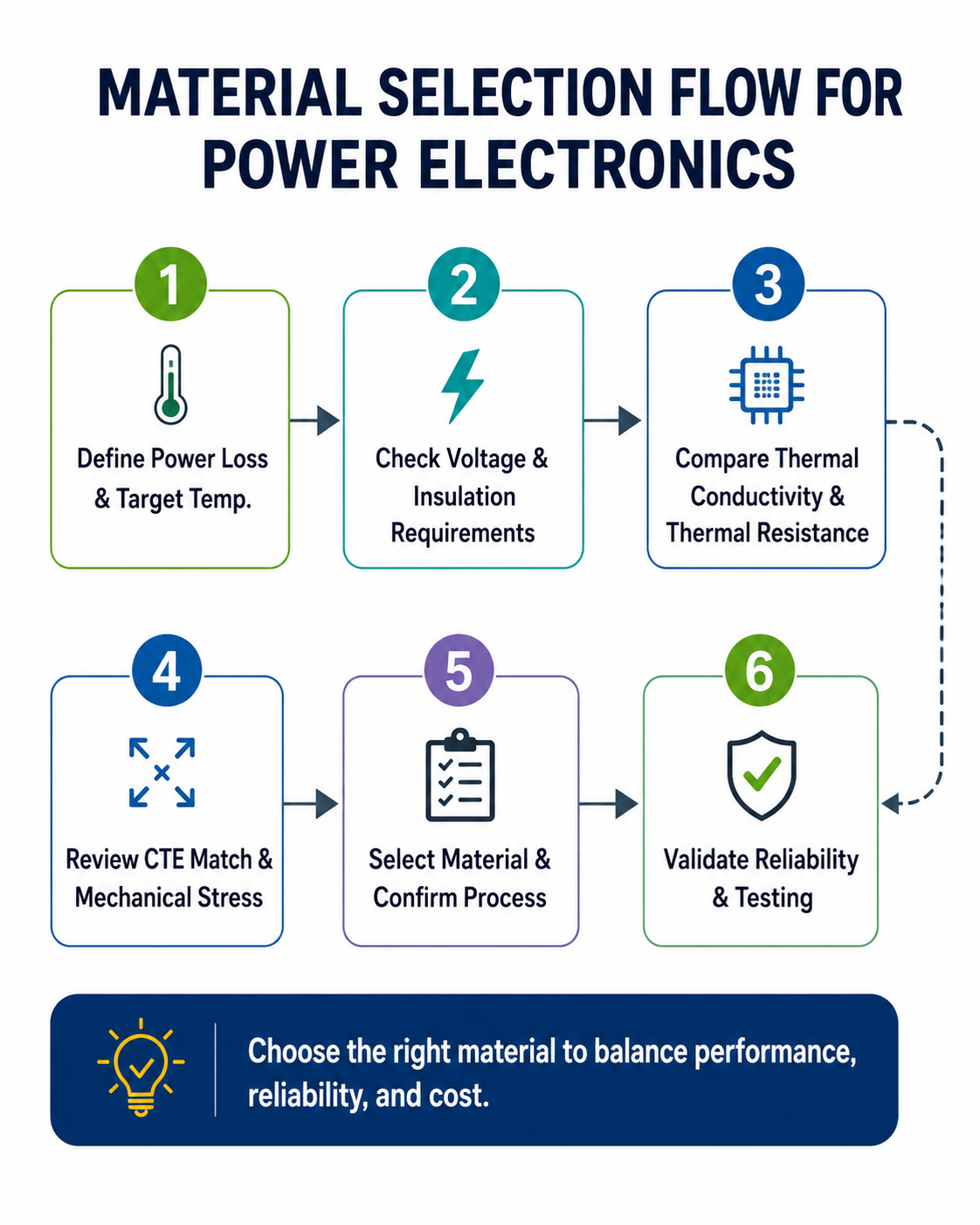
How to Choose Low Thermal Expansion Metals for Packaging and Ceramic Substrate Projects?
The right low thermal expansion metal depends on the full material stack, working temperature, package structure, and reliability target. A low CTE value is important, but it should not be the only selection factor.
| Question | Why It Matters | Direction |
|---|---|---|
| What needs matching? | Materials expand differently | Match the critical interface |
| Need heat spreading? | Some alloys conduct poorly | Consider CuW or CuMo |
| Need sealing? | Seal stress must stay low | Consider Kovar |
| Temperature range? | CTE changes with heat | Check actual range |
| Severe cycling? | Fatigue builds over time | Use compatible materials |
| Joining process? | Processes have limits | Check process fit |
| Weight limit? | W-based metals are dense | Review package limits |
| Cost target? | Low CTE metals cost more | Use where needed |
For ceramic substrate projects, the metal and ceramic should be reviewed together. Key factors include:
- Ceramic material: Al₂O₃, AlN, or Si₃N₄
- Copper thickness and copper pattern
- Substrate size and shape
- Metallization method
- Surface finish
- Soldering or brazing process
- Working temperature
- Thermal cycling requirement
- Package base or frame material
- Reliability target
For AMB and DBC ceramic substrate designs, copper thickness, ceramic thickness, metallization area, substrate size, and soldering conditions all affect stress. Low expansion metals around the package can help, but they cannot correct an unbalanced structure by themselves. Material choice, stack design, and manufacturing process must work together.
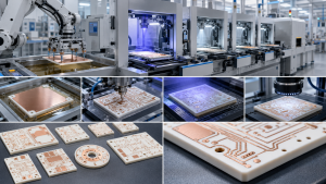
At Best Technology, ceramic substrate projects are reviewed from the application side, including substrate material, copper structure, metallization, surface finish, assembly needs, thermal path, and reliability expectations. For projects involving Al₂O₃, AlN, Si₃N₄, DBC, DPC, or AMB ceramic substrates, early material review can reduce redesign risk and improve production feasibility.
FAQs About Low Thermal Expansion Metals
What metal has the lowest thermal expansion?
Invar is one of the best-known low thermal expansion alloys near room temperature. Tungsten and molybdenum also have low CTE values and are used in high-temperature or high-stability applications.
What are the best low thermal expansion metals for electronics packaging?
Common options include Kovar, Alloy 42, molybdenum, tungsten, copper tungsten, and copper molybdenum. The best choice depends on sealing, heat spreading, temperature range, and CTE matching needs.
Why are low thermal expansion metals used with ceramic substrates?
Ceramic substrates have relatively low expansion and are brittle compared with metals. Low CTE metals reduce expansion mismatch between the ceramic and surrounding metal parts, improving thermal cycling reliability.
Is Kovar suitable for ceramic-to-metal sealing?
Yes. Kovar is widely used for glass-to-metal and ceramic-to-metal sealing because its expansion behavior matches many sealing materials.
Is copper a low thermal expansion metal?
No. Copper has excellent electrical and thermal conductivity, but its CTE is higher than many ceramics and semiconductor materials. For better CTE control, copper may be combined with tungsten or molybdenum.
What is the difference between low expansion metals and ceramic substrates?
Low expansion metals are conductive materials used for support, sealing, bases, frames, or heat spreading. Ceramic substrates are insulating circuit carriers used for electrical isolation and thermal transfer.
Are low thermal expansion metals useful for AMB or DBC ceramic substrates?
Yes, they can be useful around AMB or DBC structures, especially in bases, spreaders, frames, or supporting parts. However, the ceramic design itself must also be balanced.
How do I choose a low CTE metal for a ceramic PCB project?
Start with the ceramic material, operating temperature, thermal cycling requirement, and joining process. For sealing, Kovar may be suitable. For heat spreading and CTE control, CuW or CuMo may be better. For high-temperature stability, molybdenum or tungsten may be considered.
Can low thermal expansion metals replace ceramic substrates?
Usually, no. They serve different functions. Ceramic substrates provide insulation and circuit support. Low expansion metals provide support, sealing, or thermal spreading.
Do all electronic packages need low thermal expansion metals?
No. They are mainly used in high-power, high-temperature, hermetic, precision, or ceramic-based packages where thermal stress may affect reliability.
If you are developing an electronic package, ceramic substrate, AMB substrate, DBC substrate, or high-reliability ceramic PCB project, Best Technology can help review the material stack, thermal path, and manufacturing feasibility. Pls feel free to send your drawings, working temperature range, substrate material request, and reliability requirements to sales@bestpcbs.com for engineering support and quotation.