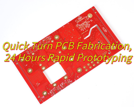
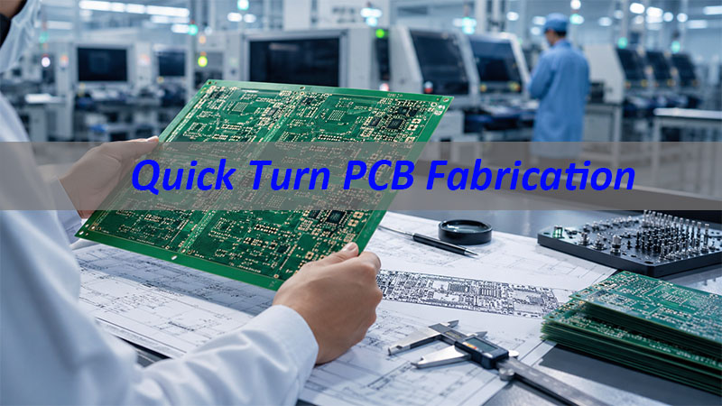
Quick turn PCB fabrication helps OEM teams move urgent projects faster, but speed alone is not enough. The real value is fast engineering review, clear manufacturability feedback, practical material confirmation, and reliable PCB delivery without creating new risks for testing, pilot runs, or production launch.
As a trustworthy quick turn PCB manufacturer, EBest Circuit (Best Technology) supports urgent OEM PCB projects with PCB fabrication, DFM review, material confirmation, surface finish options, electrical testing, and optional PCB assembly. If you need a quick turn PCB fabrication quote, please send your Gerber files, stack-up, material requirements, copper thickness, surface finish, quantity, and delivery needs to sales@bestpcbs.com. Our team will review what can be built quickly, what may need adjustment, and what could affect lead time.
What Does EBest Circuit’s Quick Turn PCB Fabrication Service Include?
EBest Circuit’s quick turn PCB fabrication service is designed for OEM projects that need faster engineering response, not just faster board production.
Our support may include:
- Gerber file review
- Stack-up and material confirmation
- DFM review before production
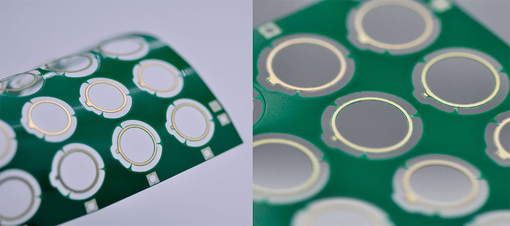
- FR4, high-Tg FR4, aluminum PCB, heavy copper PCB, HDI PCB, high-frequency PCB, and other material review
- Copper thickness confirmation
- Surface finish selection, such as HASL, lead-free HASL, ENIG, OSP, immersion tin, immersion silver, hard gold, soft gold, or ENEPIG
- Solder mask and silkscreen requirement review
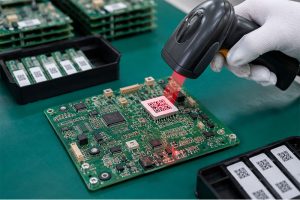
- Electrical testing
- Inspection report or special test support when required
- Optional PCB assembly support for urgent projects
This service is useful when customers need a quick turn PCB fabrication quote, but also need clear engineering communication before placing the order.
For EBEST, fast does not mean skipping review. A fast PCB order still needs correct material, manufacturable design, controlled process, and suitable testing. Otherwise, the customer may receive boards quickly but lose time later during assembly, testing, or product validation.
How We Review Files Before Quick Turn PCB Fabrication?
Before starting quick turn PCB fabrication, EBEST reviews the key manufacturing files and project details. This step helps reduce back-and-forth communication and prevents avoidable delays.
We usually check:
- Gerber files
- Drill files
- PCB stack-up
- Board thickness
- Copper thickness
- Material type
- Surface finish
- Minimum line width and spacing
- Minimum hole size
- Solder mask bridge
- Impedance requirement if needed
- Special tolerance
- Panelization requirement
- Quantity and delivery target
For urgent projects, file clarity is critical. If the Gerber data is complete, the material is available, and the process requirements are within standard capability, the project can move faster. If important information is missing, the quote may be delayed because engineering must confirm details first.
EBEST can also review whether the design is suitable for quick-turn PCB fabrication. For example, a simple double-sided PCB quick-turn fabrication project is very different from a high-layer HDI board, heavy copper board, or controlled impedance board. Each project needs a different review focus.
If your board has custom solder mask color, tight solder mask bridge, special surface finish, fine pitch BGA, blind vias, resin plugged vias, or high-current copper requirements, it is better to show these requirements clearly at the quotation stage.
What Factors Affect a Quick Turn PCB Fabrication Quote?
A quick turn PCB fabrication quote should be fast, but it must also be realistic. A low price that ignores material, tolerance, testing, or process difficulty may create delays later.
At EBEST, we prepare quotes based on the real manufacturing requirements of each board, not just board size and quantity.
Key quote factors include:
- PCB size
- Layer count
- Material grade
- Board thickness
- Copper thickness
- Minimum line width and spacing
- Minimum hole size
- Surface finish
- Solder mask requirement
- Impedance control
- HDI or blind/buried via structure
- Electrical testing requirement
- Quantity
- Delivery schedule
- PCB assembly requirement if needed
For urgent OEM projects, complete files help us quote faster and more accurately. A general request for “quick turn PCB fabrication service” is not enough for a reliable quote. Gerber files, drill files, stack-up, material notes, copper thickness, surface finish, quantity, and delivery target help our engineering team confirm what can be produced quickly and what may affect lead time.
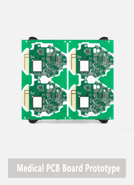
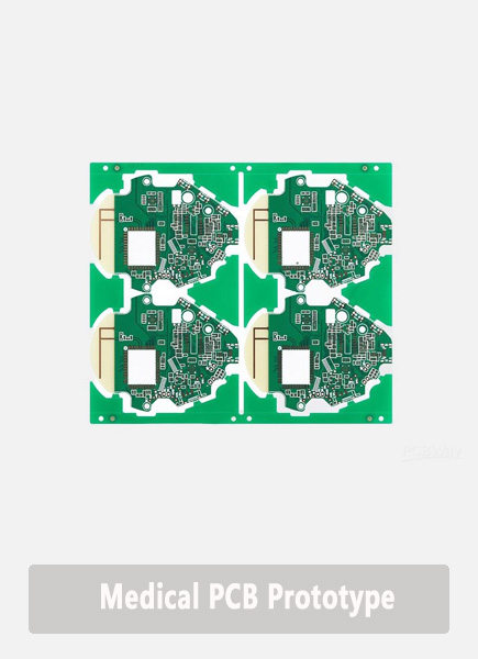
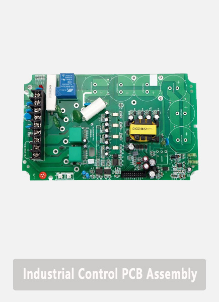
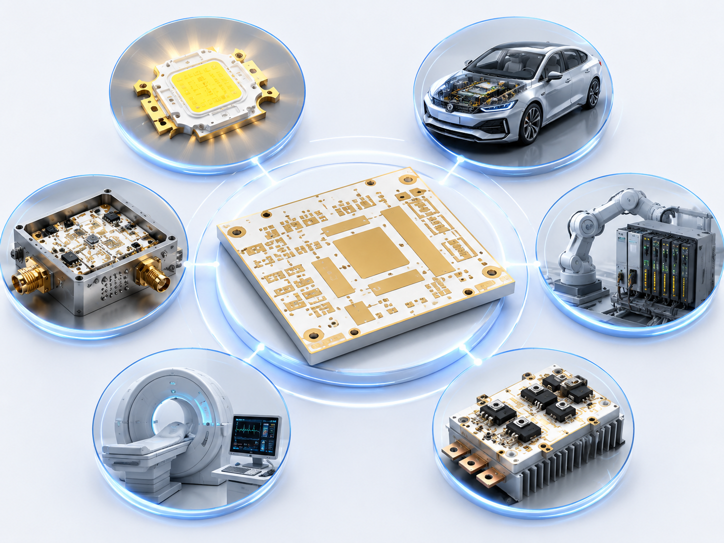
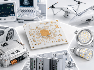
This is especially important for inverter control boards, UPS control boards, industrial control PCBs, power electronics boards, home appliance PCBs, LED boards, and communication electronics. These boards may look simple, but material, copper thickness, hole size, surface finish, and assembly requirements can strongly affect both cost and delivery.
How We Shorten PCB Lead Time Without Sacrificing Quality?
Shorter lead time should not come from removing important process controls. It should come from better preparation, clear file review, suitable material choice, and controlled production planning.
EBEST helps shorten PCB lead time through:
- Early engineering review
- Clear material confirmation
- Standard process selection when possible
- Fast clarification of unclear files
- Practical stack-up suggestions
- Suitable surface finish recommendation
- Controlled production routing
- Electrical testing before shipment
- Optional assembly planning if the project also needs PCBA
Some delays are caused not by production speed, but by unclear requirements. For example, if a customer does not confirm copper thickness, Tg value, impedance tolerance, solder mask color, or final surface finish, production cannot move smoothly.
For quick-turn PCB fabrication, our recommendation is simple: keep urgent projects manufacturable. If a design does not need a special material, special tolerance, or uncommon finish, using a practical standard process can save time. If the project truly needs special requirements, EBEST will review them before production instead of ignoring the risk.
Fast delivery is valuable only when the board is usable, testable, and suitable for the next engineering step.
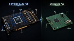
What PCB Types Can Be Supported for Quick Turn Fabrication?
EBEST can review and support different PCB types for quick turn fabrication, depending on design complexity, material availability, and process requirements.
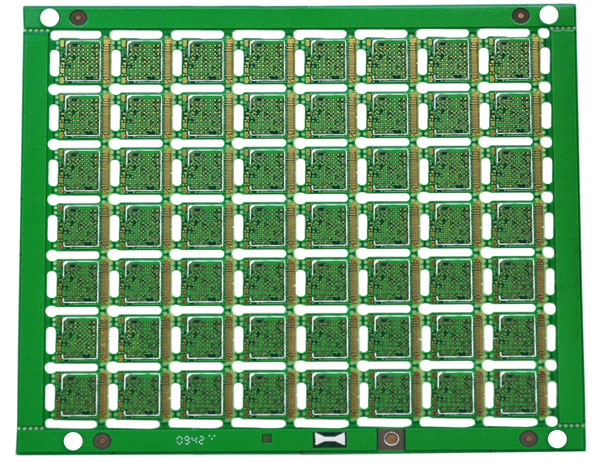
Common quick-turn PCB fabrication projects include:
- Rigid FR4 PCB
- High-Tg FR4 PCB
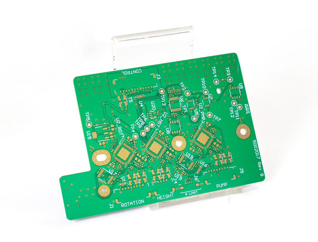
- Double-sided PCB
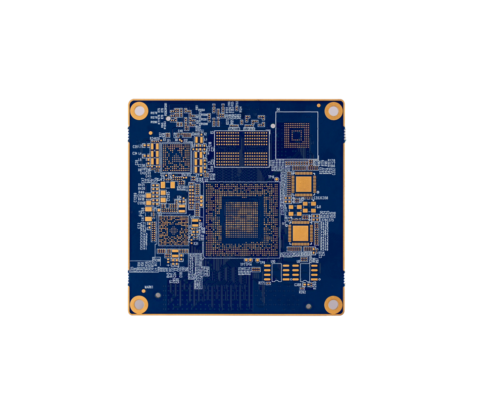
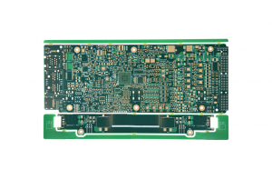
- Multilayer PCB
- Controlled impedance PCB
- Heavy copper PCB
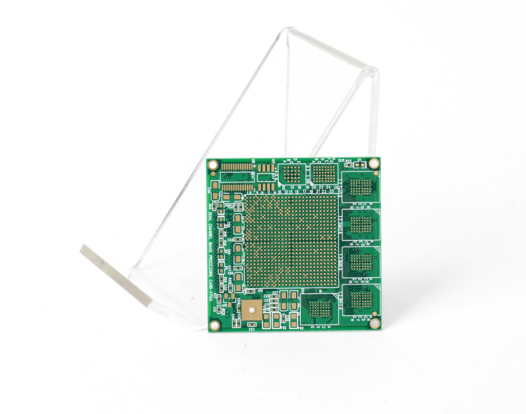
- HDI PCB
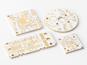
- Aluminum PCB
- Copper base PCB
- High-frequency PCB
- Rigid-flex PCB
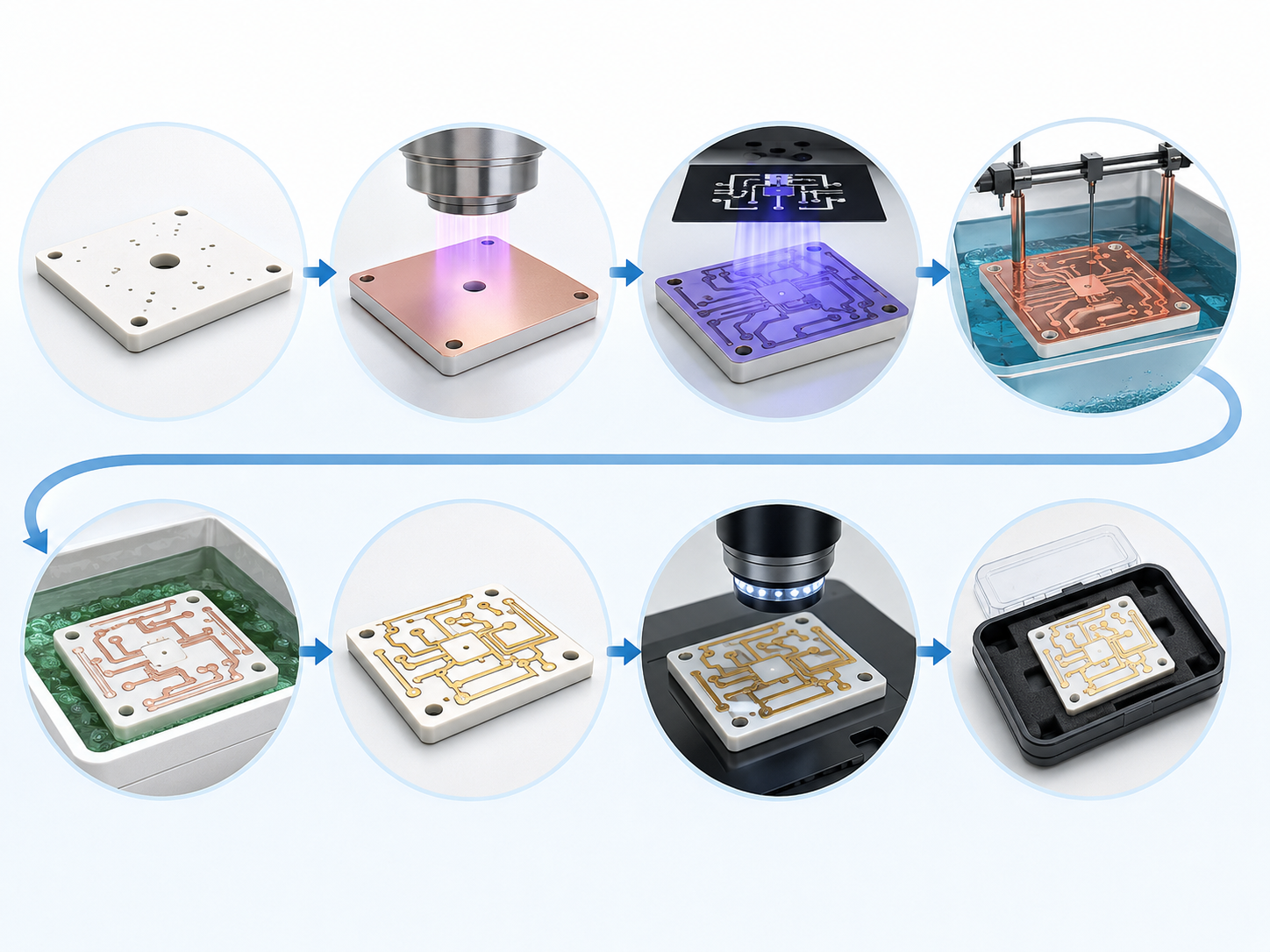
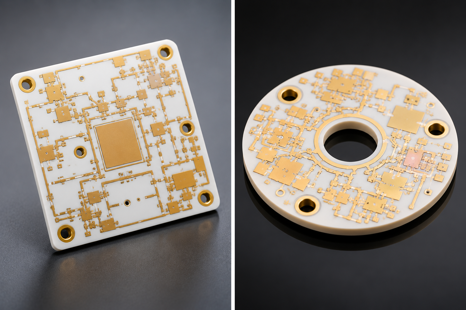
- Ceramic PCB projects after engineering review
- DPC ceramic PCB projects when the structure and schedule are suitable
For buyers searching for a quick turn rigid PCB fabricator, EBEST can support standard rigid PCB projects from simple two-layer boards to complex multilayer boards. For customers searching quick turn HDI PCB fabrication, we can review laser vias, blind vias, buried vias, microvia structure, and stack-up feasibility. For quick turn aluminum PCB fabrication, we can review metal core material, thermal conductivity, board thickness, copper thickness, and surface finish requirements.
Not every advanced PCB can be treated as a standard urgent order. HDI, heavy copper, high-frequency, ceramic, DPC ceramic, and metal core boards usually need more careful engineering review. This is why EBEST confirms project details first before promising the most realistic delivery plan.
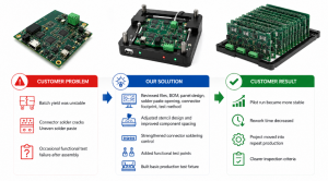
How We Support Urgent Prototype and Small-Batch OEM Projects?
Many customers do not need only one sample. They need a fast path from prototype validation to small-batch production and then repeat orders. That is why EBEST handles urgent OEM projects with a prototype-to-production mindset.
For urgent prototype and small-batch projects, we focus on:
- Fast file review
- Clear risk feedback
- Practical material selection
- Stable fabrication process
- Electrical test planning
- Repeat production feasibility
- Documentation for later batches
- Communication between engineering and purchasing teams
This is different from a sample-only approach. A sample-only supplier may focus only on making a few boards quickly. EBEST focuses on whether the board can move to the next stage after the urgent prototype is finished.
For example, if an OEM customer is developing an electronic board for inverter control, home appliance control, power management, LED lighting, medical equipment, or industrial automation, the first PCB is often only part of a larger project. The buyer may later need PCBA, functional testing, box build, packaging, or repeat production. In that situation, the quick turn PCB prototype fabricator should understand both engineering speed and production stability.
That is where EBEST’s one-stop support becomes useful.
Can EBest Circuit Combine Quick Turn PCB Fabrication and Assembly?
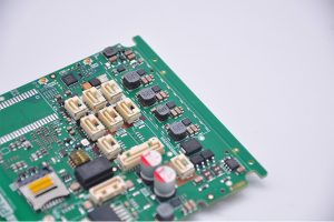
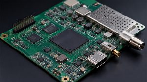
Yes. EBEST can support quick turn PCB fabrication and assembly when the customer needs both bare PCB and PCBA support.
For urgent OEM projects, PCB fabrication and assembly are often connected. A PCB may be fabricated quickly, but if component sourcing, SMT assembly, through-hole assembly, BGA assembly, testing, or stencil preparation is not planned early, the project may still be delayed.
EBEST can support:
- PCB fabrication
- Component sourcing review
- SMT assembly
- Through-hole assembly
- BGA/QFN assembly
- Connector and terminal assembly
- Stencil support
- First article inspection
- AOI inspection
- X-ray inspection when required
- Functional testing based on customer procedures
- Conformal coating or other process support when required
- Packaging and delivery coordination
For projects involving integrated circuit assembly and quick turn PCB fabrication services, early communication is especially important. IC packages, fine-pitch parts, BGAs, thermal pads, polarity marks, and test points should be reviewed before assembly starts.
A fast PCB is only useful when it can be assembled and tested smoothly. That is why EBEST encourages customers to share BOM, pick-and-place files, assembly drawings, and testing requirements as early as possible.
If your project needs PCB fabrication first and assembly later, please mention this during the quotation stage. EBEST can help review the board with the full PCBA workflow in mind.
FAQs About Quick Turn PCB Fabrication
What is quick turn PCB fabrication?
Quick turn PCB fabrication is a faster PCB manufacturing service for urgent engineering validation, prototype testing, pilot runs, small-batch production, or time-sensitive OEM projects.
What files are needed for a quick turn PCB fabrication quote?
Please send Gerber files, drill files, PCB stack-up, board thickness, copper thickness, material requirement, surface finish, quantity, and delivery target. If assembly is needed, BOM, pick-and-place file, assembly drawing, and test requirements should also be provided.
Can EBEST support both quick turn PCB fabrication and assembly?
Yes. EBEST can support PCB fabrication, component sourcing review, SMT assembly, through-hole assembly, BGA/QFN assembly, inspection, and customer-defined functional testing when required.
How can buyers reduce delays in quick turn PCB fabrication?
Send complete files, confirm material and copper thickness early, avoid unnecessary special requirements, respond quickly to engineering questions, and mention assembly or testing needs at the quotation stage.
To sum up, quick turn PCB fabrication should not be treated as a simple rush order. For urgent OEM projects, speed must work together with manufacturability, material control, process capability, testing, and communication.
EBest Circuit (Best Technology) supports customers who need more than a fast sample. We help review files, confirm materials, evaluate process risk, prepare PCB fabrication quotes, support urgent prototypes, and connect PCB fabrication with assembly when required.
If your project involves urgent PCB fabrication, HDI PCB, aluminum PCB, heavy copper PCB, rigid PCB, ceramic PCB, inverter electronics, UPS control boards, industrial electronics, medical devices, LED systems, communication products, or PCB assembly, please send your files to sales@bestpcbs.com. Our team will review your project carefully and help you move forward with a clearer manufacturing plan.