Ceramic PCB price is not decided by board size alone. It depends on ceramic material, copper structure, metallization method, circuit density, tolerance, quantity, testing scope, and the reliability level required by the final product. For engineers and buyers, the real goal is not to find the lowest unit price. The better goal is to choose a ceramic PCB structure that can handle heat, current, voltage, and long-term operating stress without overpaying for unnecessary specifications.
What Is a Ceramic PCB and Why Does Its Price Vary?
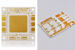
A ceramic PCB is a circuit board built on a ceramic substrate instead of conventional FR4 fiberglass material. Common ceramic materials include alumina, aluminum nitride, silicon nitride, LTCC, and HTCC ceramics. These materials are used when a product requires high thermal conductivity, strong insulation, dimensional stability, or better performance in harsh operating environments.
The price varies because “ceramic PCB” is not one single product. A simple single-sided alumina board with printed conductor is very different from an AlN DPC ceramic PCB with laser vias, fine lines, ENIG finish, and tight flatness control. A DBC power module substrate is also different from a thin-film ceramic circuit used in RF or sensor applications.
In other words, ceramic PCB price changes with the engineering requirement. The substrate, copper thickness, pattern precision, via structure, surface finish, testing requirement, yield risk, and order quantity all influence the final quotation.
Why Is Ceramic PCB Price Important for Engineering Decisions?
Ceramic PCB price matters because ceramic substrates are often used in high-value electronics. These products may include power modules, laser systems, medical electronics, RF modules, LED packages, EV components, aerospace electronics, and industrial control equipment.
In these projects, a low board price can become expensive if the material is mismatched. For example, choosing alumina only because it is cheaper may work for moderate thermal loads, but it may not be enough for a high-power module with concentrated heat. On the other hand, selecting AlN or AMB when the design does not need that level of thermal performance may increase cost without improving the final product.
A practical quotation should answer three questions: what performance is required, what reliability risk must be controlled, and what structure gives the best cost-performance balance.
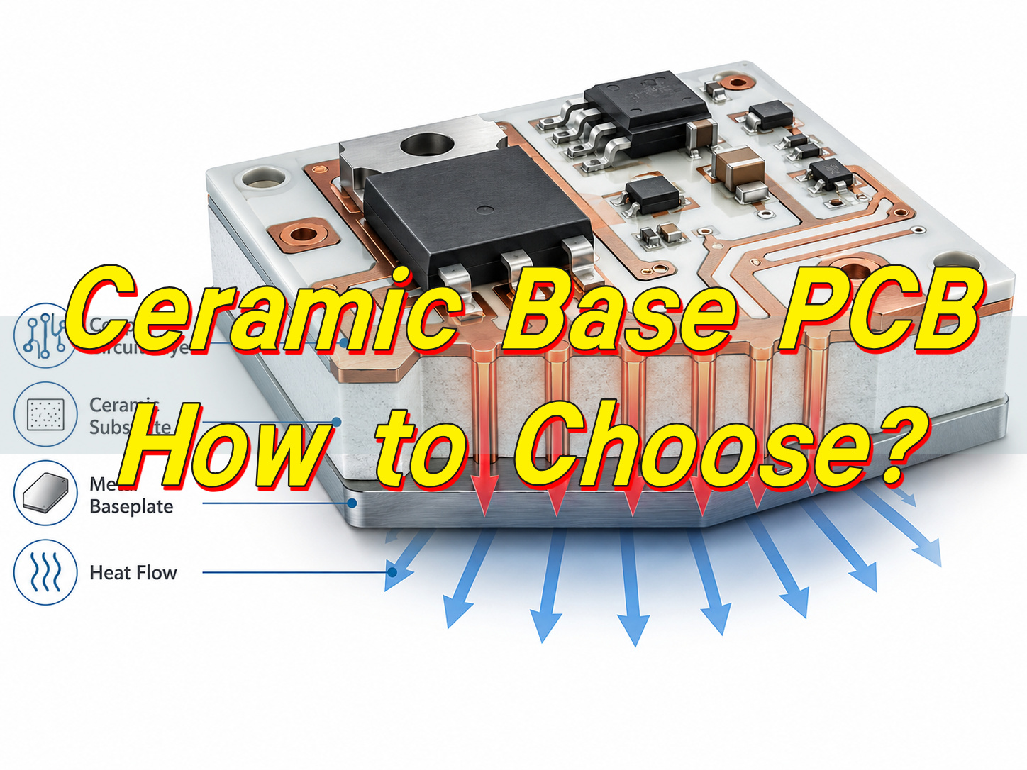
How Does a Ceramic PCB Work in Heat and Electrical Control?
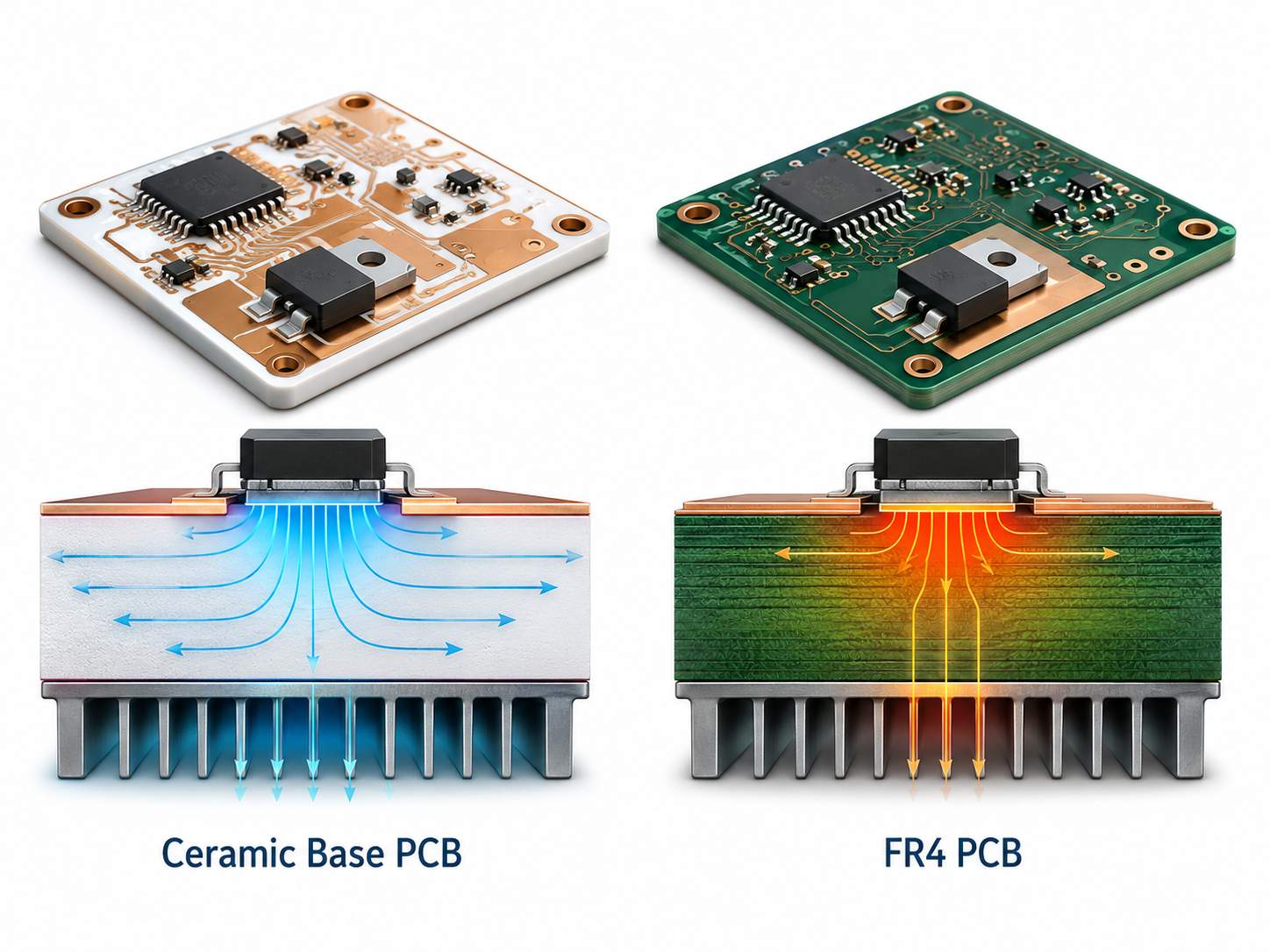
A ceramic PCB works by combining electrical insulation with efficient heat transfer. The ceramic base supports the circuit pattern while moving heat away from power components. This is why ceramic boards are widely used in thermal management applications.
In a typical high-power design, heat moves from the component pad into the copper layer, then through the ceramic substrate, and finally into the heat sink or housing. Compared with FR4, ceramic has stronger thermal stability and better dimensional behavior under heat. Compared with many metal-core PCBs, ceramic also provides excellent electrical insulation while supporting compact high-power layouts.
The working principle is simple, but the manufacturing execution is not. Copper bonding, conductor adhesion, ceramic flatness, via metallization, solderability, and thermal cycling behavior all affect reliability. These details are also part of the price.
What Types of Ceramic PCBs Have Different Cost Levels?
Different ceramic PCB technologies have different cost structures. The cheapest option is not always the best, and the most expensive option is not always necessary.
| Ceramic PCB Type | Typical Use | Cost Level | Main Price Driver |
|---|---|---|---|
| Thick film ceramic PCB | Sensors, resistors, hybrid circuits, general ceramic circuits | Low to medium | Screen printing, paste type, firing cycles |
| DPC ceramic PCB | LED, laser, power control, fine circuit ceramic boards | Medium to high | Laser vias, copper plating, line precision |
| DBC / DCB ceramic PCB | Power modules, IGBT, EV power electronics | Medium to high | Thick copper bonding and substrate size |
| AMB ceramic PCB | High-reliability power modules, EV, rail, industrial drives | High | Active metal brazing, bonding strength, thermal cycling demand |
| LTCC ceramic PCB | RF, microwave, compact multilayer modules | High | Co-fired multilayer structure and precision process |
| HTCC ceramic PCB | High-temperature packages, aerospace, military-grade electronics | High | High-temperature co-firing and metallization system |
| Thin film ceramic PCB | RF, microwave, sensors, high-precision circuits | High | Fine-line resolution and deposition control |
For price-sensitive projects, thick film or alumina DPC may be enough. For high-power cycling environments, DBC or AMB may offer better long-term value. For RF and compact module designs, LTCC or thin film may justify the higher manufacturing cost.
Which Ceramic Materials Affect Ceramic PCB Price the Most?
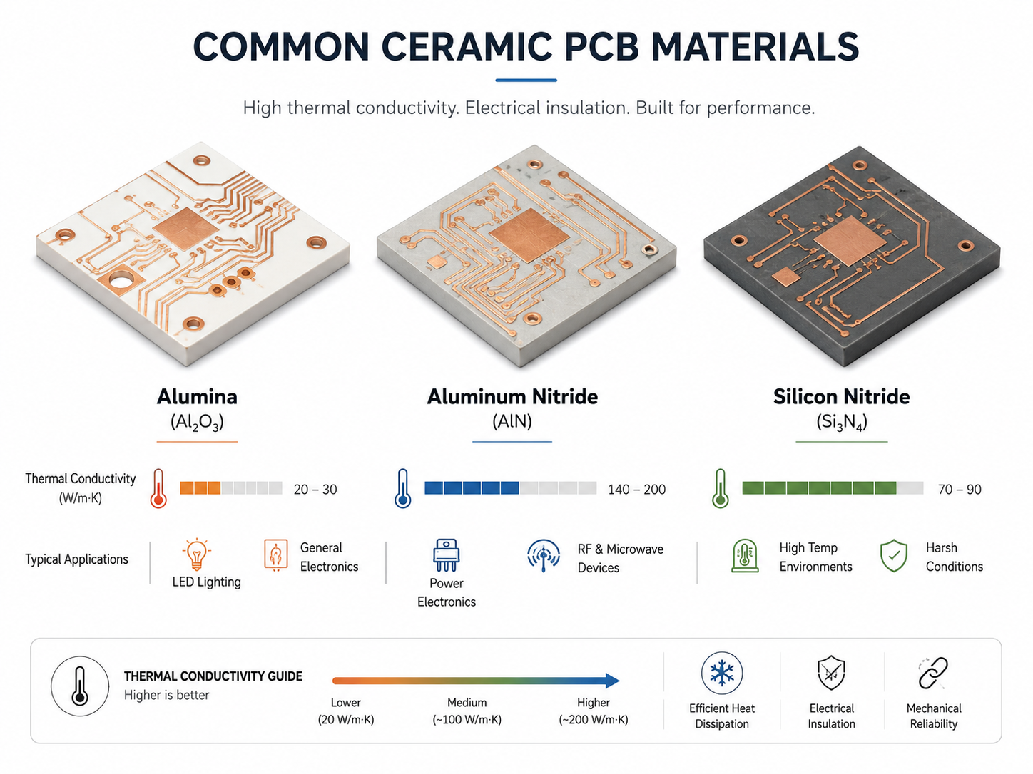
Material is one of the strongest price factors. Alumina is usually the most economical ceramic substrate. Aluminum nitride costs more because it offers much higher thermal conductivity. Silicon nitride is often selected when mechanical strength and thermal shock resistance are important.
| Material | Common Name | Typical Strength | Cost Tendency | Suitable Projects |
|---|---|---|---|---|
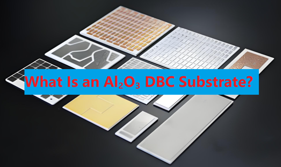
| Al₂O₃ 96% | Alumina | Stable insulation, good cost control | Lower | LED, sensors, general power electronics |
| Al₂O₃ 99% | High-purity alumina | Better electrical and surface performance | Medium | Precision circuits, medical, RF support |
| AlN | Aluminum nitride | High thermal conductivity | Higher | Laser, high-power LED, power modules |
| Si₃N₄ | Silicon nitride | Strong toughness and thermal shock resistance | Higher | EV power modules, harsh thermal cycling |
| LTCC ceramic | Low-temperature co-fired ceramic | Compact multilayer integration | Higher | RF modules, filters, sensors |
| HTCC ceramic | High-temperature co-fired ceramic | High-temperature durability | Higher | Packages, aerospace, extreme environments |
Alumina is often selected when the project needs ceramic stability but does not require extreme heat transfer. AlN is selected when thermal resistance must be reduced. Si₃N₄ is often considered when cracking, delamination, or thermal cycling risk is more important than the lowest starting price.
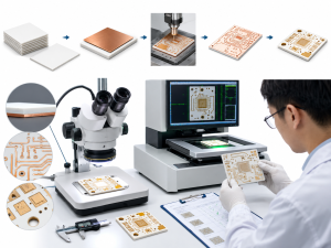
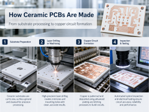
What Manufacturing Processes Change the Final Quote?
The process route can change the price more than the material itself. A small ceramic PCB with simple printed conductors may be relatively economical. The same size board with laser-drilled vias, plated copper, fine-line patterning, and strict inspection can cost much more.
Key manufacturing cost drivers include ceramic cutting, laser drilling, via filling, copper deposition, electroplating, screen printing, firing, photolithography, surface treatment, inspection, and packaging. Fine circuit spacing increases yield pressure. Tight dimensional tolerance requires more process control. Double-sided or multilayer structures add alignment difficulty.
Surface finish also matters. ENIG, gold plating, silver conductor, nickel barrier layers, and special solderable finishes each have different cost implications. For high-reliability applications, the surface finish should be selected based on soldering, wire bonding, storage time, and working environment.
How Do Ceramic PCBs Compare With FR4, MCPCB, DPC, DBC, and AMB?
Ceramic PCB price should not be judged in isolation. It should be compared with the full thermal and reliability requirement of the product.

| Option | Price Level | Thermal Performance | Insulation | Best Fit |
|---|---|---|---|---|
| FR4 PCB | Low | Low to medium | Good | Standard electronics |
| High-Tg FR4 | Low to medium | Medium | Good | Higher soldering or operating temperature |
| Aluminum MCPCB | Medium | Medium to good | Depends on dielectric layer | LED lighting and moderate heat dissipation |
| Copper substrate PCB | Medium to high | Very good | Depends on insulation system | High-power thermal designs |
| Alumina ceramic PCB | Medium | Good | Excellent | Compact thermal and insulation applications |
| AlN ceramic PCB | High | Excellent | Excellent | High-power and heat-critical designs |
| DPC ceramic PCB | Medium to high | Good to excellent | Excellent | Fine circuits, vias, LEDs, laser modules |
| DBC ceramic PCB | Medium to high | Excellent for power modules | Excellent | Thick copper and high current |
| AMB ceramic PCB | High | Excellent | Excellent | High thermal cycling reliability |
FR4 wins on cost. MCPCB works well for many lighting and moderate thermal applications. Ceramic PCB becomes valuable when heat, insulation, stability, compactness, or long-term reliability cannot be solved by conventional materials.
How Should Engineers Choose the Right Ceramic PCB Option?
Engineers should start with operating conditions, not only price. The most important details include power density, junction temperature target, insulation voltage, current load, copper thickness, line width, component package, soldering process, and product lifetime.
For a high-power LED module, alumina DPC may be suitable if the heat load is manageable. For a laser diode module, AlN may be preferred because heat concentration is usually higher. For an IGBT or SiC power module, DBC or AMB may be more practical because thick copper and bonding reliability become critical.
The best choice is usually the lowest-cost structure that still meets the thermal, electrical, mechanical, and reliability requirements. Over-specification increases cost. Under-specification increases failure risk.
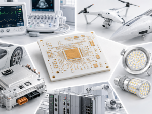
Where Are Ceramic PCBs Used in Real Industry Projects?
Ceramic PCBs are used in industries where thermal management, insulation, or high-reliability operation is important.
In LED and lighting products, ceramic substrates help transfer heat away from high-brightness chips. In laser modules, they support stable heat spreading and precise assembly. In automotive electronics, ceramic substrates are used in power control, EV charging, battery systems, and high-temperature electronics. In medical electronics, ceramic PCBs may be used in sensors, diagnostic equipment, and compact modules requiring stable electrical behavior.
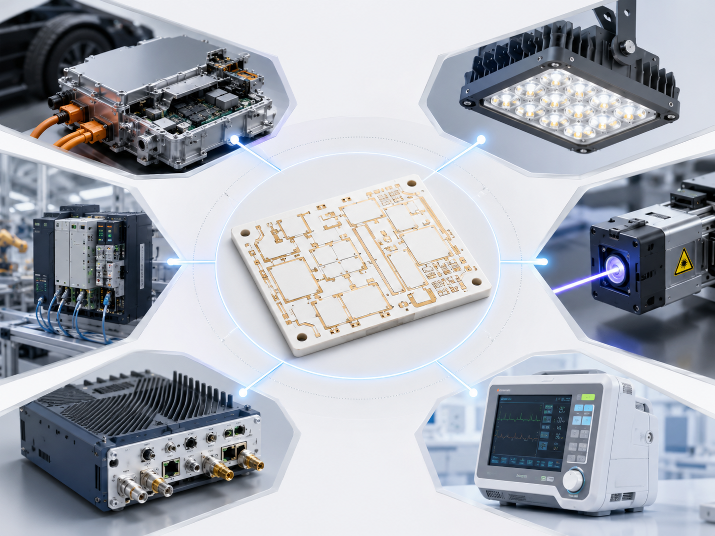
RF and microwave applications may use ceramic circuits because of dielectric stability and low signal loss. Industrial equipment uses ceramic boards in power supplies, motor drives, heating systems, and harsh-environment control modules. Aerospace and defense applications may use ceramic substrates where vibration, heat, and long-term reliability are part of the design requirement.
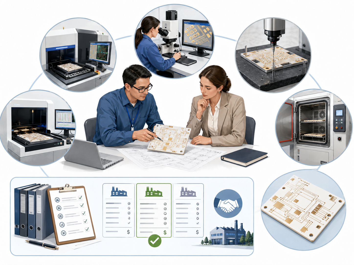
What Should Be Checked Before Ceramic PCB Fabrication?
Before requesting a ceramic PCB price, buyers should prepare more than Gerber files. A complete quotation package helps the manufacturer evaluate cost accurately and avoid repeated engineering questions.
Useful quotation details include substrate material, ceramic thickness, copper thickness, board size, quantity, surface finish, line width, spacing, hole size, via type, tolerance, solder mask or glass coating requirement, working temperature, insulation voltage, and assembly method. If the board will be wire bonded, the bonding area finish should be clearly specified.
Engineers should also confirm whether the board needs DFM review, impedance evaluation, thermal simulation support, special packaging, 100% electrical test, or reliability testing. These requirements may affect both price and lead time.
How Do Testing and Quality Standards Affect Cost?
Testing increases cost, but it also reduces risk. For ceramic PCBs, common inspections may include visual inspection, dimensional measurement, adhesion test, continuity test, insulation resistance test, solderability check, metallization thickness measurement, thermal shock test, and X-ray inspection for selected structures.
For general PCB quality control, IPC-6012 is widely used for rigid printed board qualification and performance requirements, while IPC-A-600 is commonly used for visual acceptability criteria. IPC-TM-650 provides test methods used across PCB reliability and material evaluation. These standards are not a simple “price add-on”; they help define what acceptable quality means before mass production starts.
For ceramic PCBs, the testing plan should match the application. A prototype for lab verification may not need the same testing as an EV power module or medical device assembly. However, skipping essential checks can create hidden cost later.
What Failure Modes Can Increase Hidden Cost?
The visible ceramic PCB price is only one part of project cost. Hidden cost often appears when a board fails during assembly, reliability testing, or field operation.
Common failure modes include ceramic cracking, copper peeling, poor solder wetting, via voids, conductor open circuits, copper-to-ceramic delamination, thermal cycling fatigue, surface contamination, and edge chipping. These failures may come from material mismatch, excessive copper stress, unsuitable surface finish, poor laser drilling quality, aggressive handling, or insufficient process control.
For power applications, copper thickness and ceramic material must be balanced carefully. Thick copper improves current capacity, but it can also increase thermal stress during temperature cycling. For fine circuits, the main risk may be line defects, poor adhesion, or via reliability. A good supplier should review these risks before production, not after failure analysis.
How Can Buyers Control Ceramic PCB Price Without Reducing Reliability?
The most effective way to control ceramic PCB price is to avoid unnecessary specifications while protecting critical performance. Buyers should separate “must-have” requirements from “nice-to-have” requirements.
For example, do not request AlN if alumina can meet the thermal target. Do not specify ultra-tight tolerances if the assembly does not need them. Do not use thick copper if current and thermal performance can be achieved with a thinner copper structure. Do not request complex double-sided vias when a single-sided layout can work.

Quantity also affects unit price. Prototype orders carry setup, engineering, tooling, and process preparation cost. Larger batches spread these costs across more boards. If the design is still changing, it is better to start with a controlled prototype, validate performance, then move to optimized batch production.
A practical quotation strategy is to ask for two options: one engineering-safe option and one cost-optimized option. This helps buyers compare price, risk, and production feasibility clearly.
Ceramic PCB Price FAQ
How much does a ceramic PCB cost?
Ceramic PCB cost varies widely because the product can range from a simple alumina substrate to a high-reliability AMB or LTCC multilayer circuit. Board size, material, copper thickness, process type, quantity, surface finish, and testing scope all affect pricing. For custom projects, a reliable supplier usually needs Gerber files, material requirements, quantity, and application details before giving an accurate quote.
Why is ceramic PCB more expensive than FR4 PCB?
Ceramic PCB is more expensive because the raw material is costlier and the manufacturing process is more specialized. Ceramic cutting, laser drilling, metallization, firing, copper bonding, and precision inspection require dedicated equipment and process control. FR4 is suitable for many standard electronics, but ceramic is used when heat, insulation, dimensional stability, or harsh-environment reliability becomes more important than the lowest board price.
Is alumina ceramic PCB the cheapest option?
In most ceramic PCB projects, alumina is the most cost-friendly ceramic substrate. It offers good insulation, stable mechanical properties, and acceptable thermal performance for many LED, sensor, and power control applications. However, alumina is not always the best choice. If the design has high heat concentration or strong thermal cycling stress, AlN, Si₃N₄, DBC, or AMB may provide better long-term reliability.
When should I choose AlN ceramic PCB?
AlN ceramic PCB is suitable when thermal conductivity is a key design requirement. It is often used in laser modules, high-power LEDs, RF power devices, power electronics, and compact thermal designs. Buyers should choose AlN when alumina cannot meet the thermal target. If the heat load is moderate, alumina may still be a more economical choice.
Does copper thickness affect ceramic PCB price?
Yes. Copper thickness affects raw material cost, process difficulty, etching control, plating time, bonding stress, and reliability behavior. Thicker copper can support higher current and better heat spreading, but it may increase stress between copper and ceramic during thermal cycling. The right copper thickness should be selected according to current load, heat path, pad structure, and reliability target.
Is DPC cheaper than DBC?
DPC and DBC have different cost logic. DPC is often used for fine circuits, plated vias, and thinner copper structures. DBC is preferred for power modules that need thick copper and strong current capacity. One is not always cheaper than the other. The final price depends on material, copper thickness, circuit complexity, size, quantity, and testing requirement.
What information is needed for a ceramic PCB quote?
A complete quote should include Gerber files, substrate material, ceramic thickness, copper thickness, board size, quantity, surface finish, tolerance, via requirement, solder mask or coating, working temperature, insulation voltage, and application background. If the product has high reliability requirements, share the thermal cycling, vibration, humidity, or assembly conditions as early as possible.
Can ceramic PCB reduce total product cost?
Yes, in the right application. Ceramic PCB may have a higher board price, but it can reduce heat sink size, improve reliability, simplify thermal design, and lower failure-related cost. For power electronics, LEDs, lasers, and compact modules, the value often comes from system-level performance rather than the bare PCB price alone.
Why do two suppliers give very different ceramic PCB prices?
Different suppliers may quote different materials, process routes, copper thicknesses, finishes, tolerances, testing levels, or lead times. Some quotes may include engineering review and full inspection, while others only cover basic fabrication. Buyers should compare the technical details behind each quote, not only the final number. A low quote with unclear specifications can create production risk.
Is ceramic PCB suitable for high-volume production?
Yes, ceramic PCB can be used for volume production when the design is stable and the process is validated. The key is to control material consistency, metallization quality, dimensional tolerance, yield, packaging, and batch traceability. For high-volume orders, early DFM review and prototype validation help reduce scrap, rework, and late-stage design changes.
How can I reduce ceramic PCB price during design review?
The best methods include simplifying the circuit layout, choosing the right material grade, avoiding unnecessary tight tolerances, optimizing panel utilization, reducing special surface finish requirements, and selecting a process that matches the application. Buyers can also request prototype and batch pricing separately. This helps control early development cost while preparing for scalable production.
What quality checks are important for ceramic PCB orders?
Important checks include dimensional inspection, visual inspection, copper thickness measurement, adhesion verification, electrical continuity, insulation resistance, solderability, and packaging inspection. For demanding applications, thermal cycling, thermal shock, X-ray inspection, and cross-section analysis may be added. The testing plan should match the product risk level instead of using the same checklist for every project.
Conclusion:
Ceramic PCB price should be evaluated as an engineering decision, not only a purchasing number. The right choice depends on material, process, copper structure, reliability target, testing scope, and production volume.
Before placing an order, it is better to share complete Gerber files, material requirements, quantity, and application conditions with an experienced ceramic PCB manufacturer for DFM review and cost optimization.
If you need ceramic PCB prototypes, custom ceramic substrates, small-batch production, or mass manufacturing support, feel free to contact our engineering team. Email: sales@bestpcbs.com