PCB manufacturing PCB manufacturing
Home > Blog

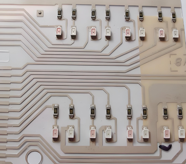
Ceramic PCB Assembly

Ceramic PCB Assembly Service China, Ceramic PCB Manufacturer
Friday, May 29th, 2026

What Is Ceramic PCB Assembly?

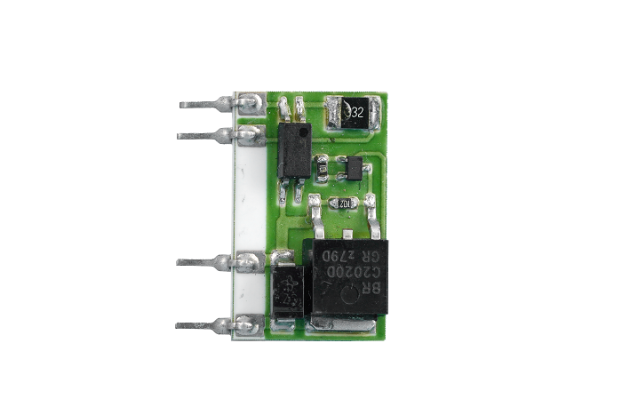
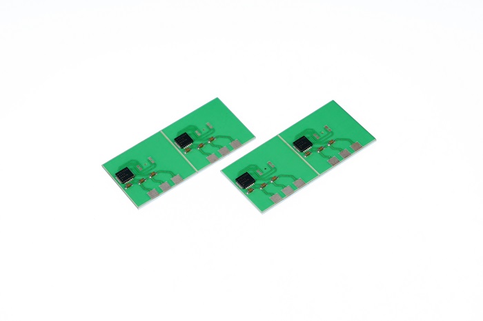
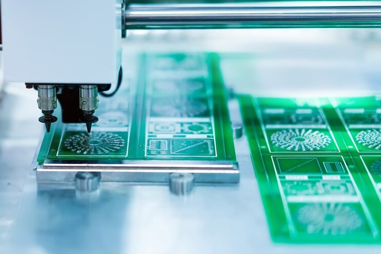
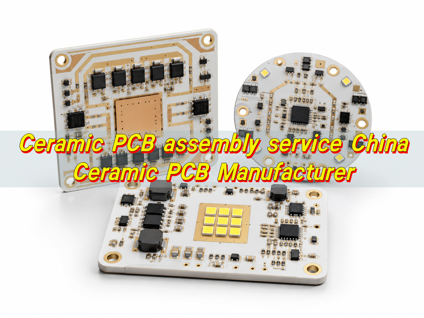
Ceramic PCB assembly is the process of mounting electronic components onto a ceramic PCB board and turning it into a working electronic module. The process may include solder paste printing, SMT placement, reflow soldering, through-hole assembly, inspection, electrical testing, functional testing, and final packaging.
Ceramic PCB Assembly Service China, Ceramic PCB Manufacturer

A ceramic PCB is used when a product needs better heat transfer, stable insulation, high dimensional stability, or reliable performance in compact power circuits. These boards are widely used in LED modules, power supplies, automotive electronics, RF products, laser devices, medical equipment, industrial controls, and high-temperature electronics.

Typical FR4 has thermal conductivity of about 0.3 W/m·K. Alumina ceramic is commonly around 24–30 W/m·K, while aluminum nitride can reach about 140–180 W/m·K depending on grade and supplier.

EBest Circuit (Best Technology) supports ceramic PCB fabrication, component sourcing, SMT assembly, through-hole assembly, inspection, and testing. For ceramic projects, the engineering team usually reviews material selection, copper structure, component package, soldering method, and test requirements before production.

How Is Ceramic PCB Assembly Different from Standard PCB Assembly?

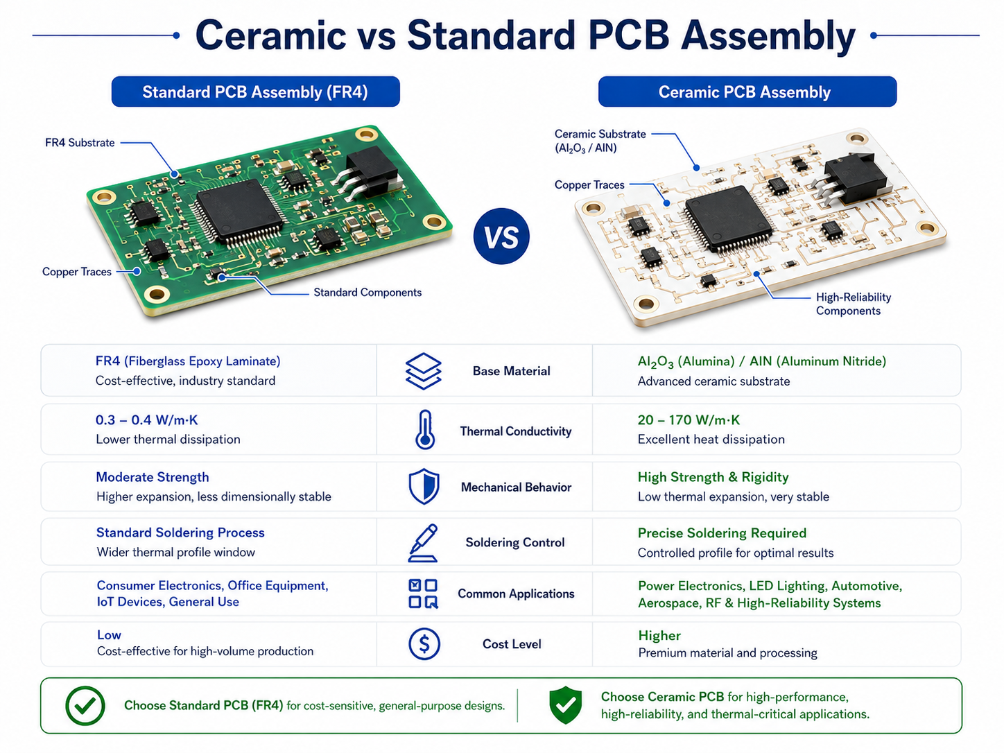
Ceramic PCB assembly follows many standard PCBA steps, but the process control is more specific. Standard FR4 boards have moderate flexibility and are easier to handle during panel processing, component insertion, and depaneling. Ceramic boards are dimensionally stable and thermally efficient, but they require more careful handling because the substrate is rigid and brittle.
Ceramic PCB Assembly Service China, Ceramic PCB Manufacturer

The copper structure can also be different. Ceramic boards may use DPC, DBC, AMB, thick-film, or thin-film technology. Each process has different copper thickness, line capability, bonding strength, and cost. For example, DBC is often used in power modules because it supports thicker copper and efficient thermal transfer. DPC is often used when fine lines and accurate metallization are required.

ItemStandard FR4 PCB AssemblyCeramic PCB Assembly
Base materialGlass fiber epoxy laminateAlumina, aluminum nitride, silicon nitride, or other ceramic substrate
Thermal conductivityUsually around 0.3 W/m·KCommonly from 24 W/m·K to over 170 W/m·K
Mechanical behaviorMore flexibleRigid and requires careful handling
Soldering controlWider process windowRequires more accurate thermal profiling
Copper structureStandard etched copper layersDPC, DBC, AMB, thick-film, or thin-film structures
Common applicationsGeneral electronicsPower, LED, RF, automotive, medical, aerospace, and industrial electronics
Cost levelLower material and processing costHigher substrate, fabrication, and handling cost
Inspection focusPlacement, solder joints, polarity, electrical testSolder joints, voids, cracks, copper adhesion, thermal pads, edge condition

The main value of ceramic boards is performance under thermal, electrical, or mechanical demand. The main requirement is disciplined process control. When both are matched, ceramic assemblies can provide stable performance in applications where FR4 may not be suitable.

Can Through-Hole Components Be Used on Ceramic PCBs?

Through-hole components can be used on ceramic PCBs when the hole structure, lead size, soldering method, and mechanical stress are properly reviewed. Although many ceramic pcb boards use SMT components, some products still require pin headers, terminals, connectors, sensors, fuses, or power pins.

Hole formation in ceramic materials is different from FR4 processing. Depending on the material, board thickness, and hole diameter, holes may be made by laser drilling, mechanical drilling, or other ceramic-specific methods. If the hole needs electrical connection, the inner wall must be metallized. Hole tolerance, copper adhesion, and plating quality should be checked before production.

Through-hole assembly is often used in these ceramic PCB applications:

  • Power modules with high-current pins or screw terminals.
  • LED driver boards with power input and control connectors.
  • Sensor modules requiring stable external wiring.
  • High-voltage boards using leaded components with controlled spacing.
  • Hybrid assemblies combining SMT parts and through-hole parts.

The soldering method depends on design and volume. Selective soldering, manual soldering, pin-in-paste reflow, or fixture-assisted soldering may be used. The process should control heat input and reduce mechanical force. For heavy components, mechanical support may be needed so the solder joints do not carry the full load during product use.

EBest Circuit (Best Technology) reviews through-hole ceramic designs by checking hole size, substrate thickness, copper structure, solder access, connector load, and inspection requirements.

What Files Are Needed for Ceramic PCB Assembly?

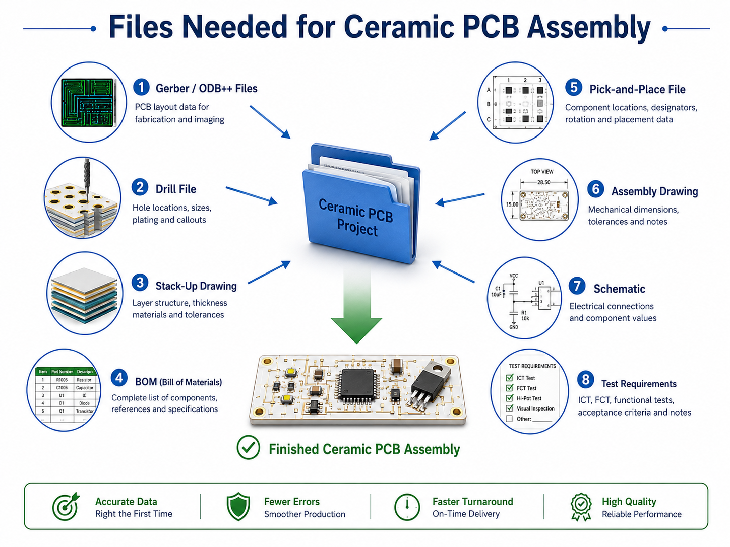
A complete file package helps the manufacturer quote, fabricate, assemble, and test the product correctly. For ceramic PCB assembly, the files should show not only the circuit layout but also the material, copper structure, component position, soldering notes, and test method.

For a ceramic pcb prototype, basic files may be enough for early quotation. For production, the documentation should be more complete, especially for power electronics, medical devices, automotive electronics, aerospace products, and industrial control modules.
Ceramic PCB Assembly Service China, Ceramic PCB Manufacturer

A practical file package usually includes:

  • Gerber files or ODB++ files for PCB fabrication.
  • Drill files for plated holes, non-plated holes, and slots.
  • Stack-up drawing showing ceramic material, board thickness, copper thickness, and surface finish.
  • BOM with manufacturer part number, package, quantity, tolerance, and approved alternatives.
  • Pick-and-place file with coordinates and rotation.
  • Assembly drawing showing polarity, orientation, special notes, and keep-out areas.
  • Schematic for engineering review and test planning.
  • Stencil requirements if solder paste aperture control is already defined.
  • Test instructions for electrical test, functional test, programming, high-voltage test, or thermal test.
  • Quality requirements such as IPC class, RoHS/REACH request, inspection criteria, and traceability level.
File TypePurposeWhy It Matters
Gerber or ODB++Defines circuit patternConfirms pad geometry, copper area, spacing, and fabrication data
Drill fileDefines holes and slotsSupports ceramic drilling and metallization review
Stack-up drawingDefines material and thicknessAffects heat transfer, insulation, RF behavior, and mechanical strength
BOMDefines componentsSupports sourcing, assembly preparation, and alternative review
Pick-and-place fileGuides SMT placementReduces rotation and position errors
Assembly drawingShows component orientation and notesHelps manual inspection and special process control
SchematicExplains circuit functionSupports DFM review, testing, and troubleshooting
Test documentDefines acceptance methodConfirms how the finished assembly will be verified

For ceramic pcb assembly service China projects, many overseas customers send partial information at the first RFQ stage. That is acceptable for budgetary review. Before production, the manufacturer should confirm all critical data.

EBest Circuit (Best Technology) can review the file package before production and provide feedback on manufacturability, BOM availability, component alternatives, and test planning.

What Should Be Checked Before Ceramic PCB Assembly?

Before assembly starts, the engineering team should confirm whether the design matches the selected ceramic material and production process. Ceramic boards are often used in high-value applications, so early checks can save time during prototype validation and batch production.

The first item is material selection. Alumina is widely used because it offers good insulation, stable performance, and controlled cost. Aluminum nitride is selected when heat dissipation is a major requirement. Silicon nitride is used in some demanding power and automotive applications because it offers good mechanical strength and thermal shock resistance.

The second item is copper structure. Copper thickness, line width, spacing, bonding method, and surface finish must match current load, heat transfer, insulation distance, and soldering requirements. For high-current circuits, thick copper may be required. For fine-pitch circuits, DPC or thin-film ceramic technology may be more suitable.

Pad design should also be reviewed. Large thermal pads can create solder voids if stencil openings are not optimized. Small pads may reduce solder joint strength or thermal transfer. For LEDs, QFN, LGA, MOSFETs, and power ICs, the stencil design, solder paste volume, and thermal pad layout should be checked together.

The BOM should be verified before SMT preparation. The review should cover package type, polarity, MSL level, lead time, lifecycle status, and substitute options.

Key pre-assembly checks include material grade, board thickness, copper thickness, surface finish, pad size, stencil aperture, component orientation, fixture design, handling method, reflow profile, cleaning requirement, test access, and traceability requirement. For high-voltage products, creepage and clearance should be reviewed. For RF products, impedance, dielectric constant, grounding structure, and connector transition should be checked.

EBest Circuit (Best Technology) provides DFM review for ceramic PCB and PCBA projects. The review focuses on practical production points, including material choice, soldering feasibility, component sourcing, inspection access, and testing method.

What Soldering Process Is Used for Ceramic PCB Assembly?

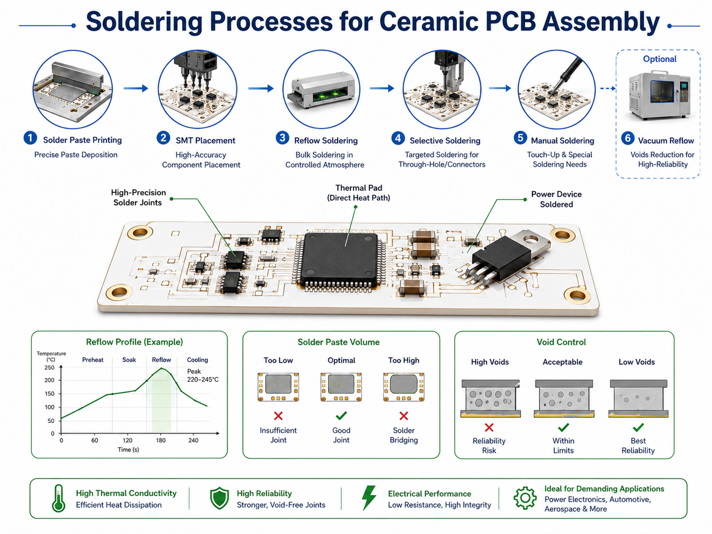
The soldering process depends on substrate material, copper structure, component type, board thickness, thermal mass, surface finish, and production volume. Most ceramic PCB assemblies use SMT reflow soldering for surface mount parts. Some products also require selective soldering, manual soldering, pin-in-paste reflow, vacuum reflow, or fixture-assisted soldering.
Ceramic PCB Assembly Service China, Ceramic PCB Manufacturer

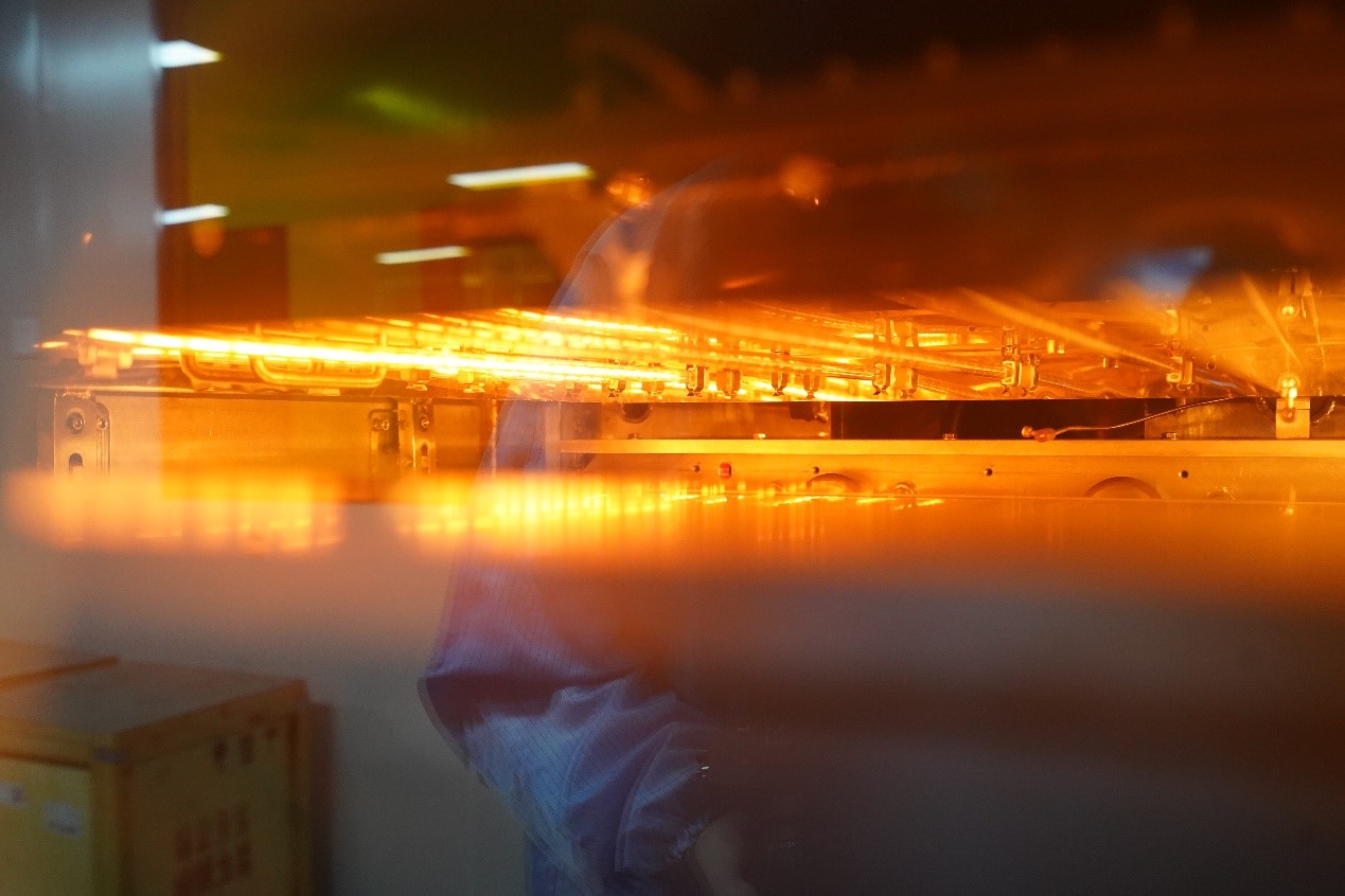
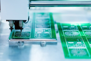
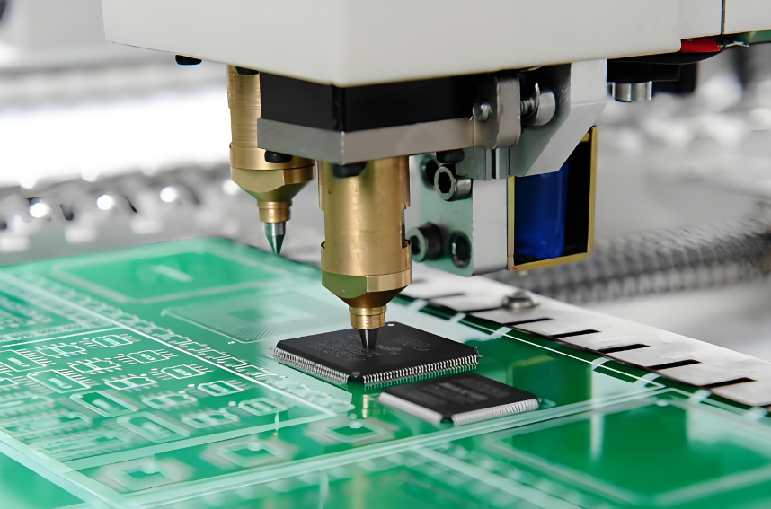
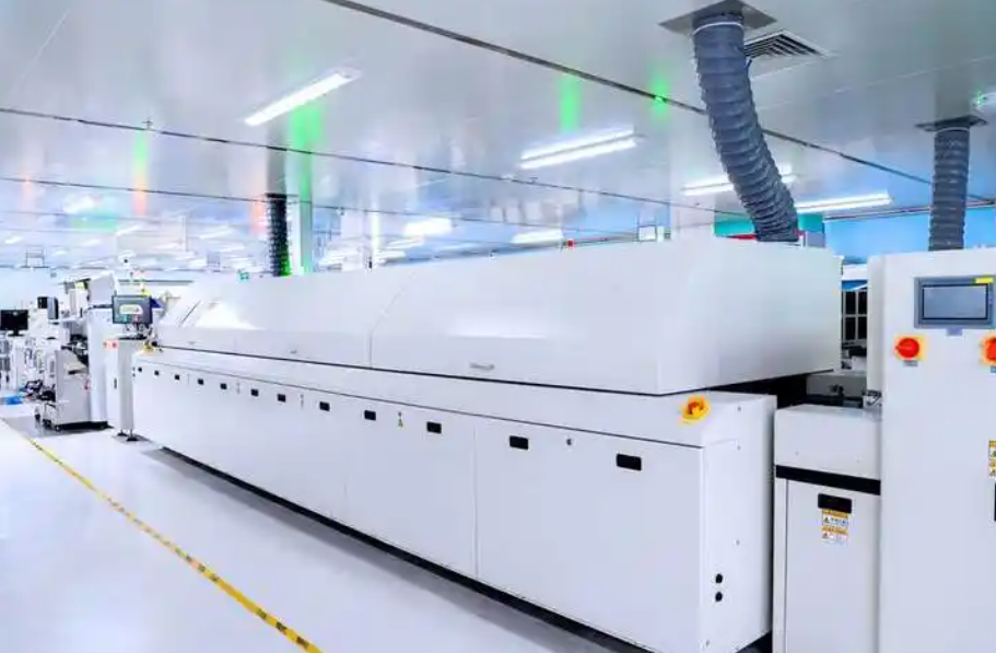
SMT reflow is used for LEDs, ICs, resistors, capacitors, sensors, RF parts, and many power devices. The process starts with solder paste printing. Components are then placed by SMT equipment, and the board passes through a controlled reflow oven.

Soldering MethodTypical UseKey Control Point
SMT reflow solderingLEDs, ICs, resistors, capacitors, sensors, RF partsReflow profile, solder paste volume, thermal balance
Selective solderingThrough-hole connectors, terminals, and pinsLocal heating, hole fill, substrate stress
Manual solderingPrototype, low-volume, special componentsTip temperature, contact time, operator consistency
Pin-in-paste reflowThrough-hole pins assembled during SMTPaste volume, lead length, hole fill
Vacuum reflowPower modules and large thermal padsVoid reduction under hidden pads
Fixture-assisted solderingSpecial structures or heavy componentsAlignment, stability, and heat uniformity

Solder paste selection should match surface finish, component terminal plating, and reliability requirements. Lead-free SAC solder is common, while high-temperature solder or special alloys may be used for certain power or harsh-environment applications. Flux residue requirements should also be confirmed, especially for high-voltage, RF, medical, and clean electronic assemblies.

How Are Ceramic PCB Assemblies Tested?

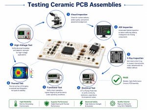
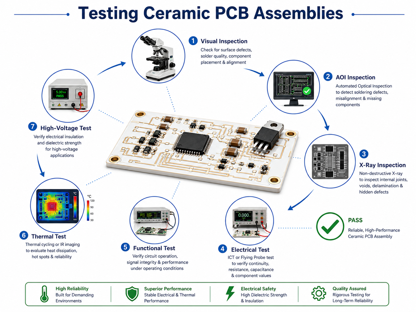
Ceramic PCB assemblies are tested through visual inspection, AOI, X-ray inspection, electrical test, functional test, and application-specific verification. The test plan depends on circuit function, product risk, industry requirement, and customer acceptance criteria.

Visual inspection checks ceramic edges, surface condition, component placement, solder appearance, polarity, marking, contamination, and mechanical damage. Since ceramic substrates are rigid, edge chips and cracks should be checked carefully.

AOI is used after SMT reflow to check missing parts, wrong parts, offset, polarity, tombstoning, solder bridges, and visible solder issues. AOI is efficient for visible components, but it cannot inspect hidden solder joints under BGA, QFN, LGA, or large thermal pads.

X-ray inspection is useful for hidden joints and large thermal pads. It helps identify solder voids, bridging, insufficient solder, and alignment problems.
Ceramic PCB Assembly Service China, Ceramic PCB Manufacturer

Electrical testing confirms continuity, isolation, and circuit behavior. Depending on the design, the test may include open/short test, insulation resistance test, high-voltage test, current test, programming, communication check, or full functional test. RF ceramic boards may require impedance-related checks, return loss, insertion loss, or frequency response testing based on product requirements.

Test MethodWhat It ChecksTypical Use
Visual inspectionSurface condition, solder appearance, ceramic edges, polarityFirst-level quality control
AOIPlacement, missing parts, solder bridges, polaritySMT process verification
X-rayHidden joints, voids, BGA/QFN/LGA solderingPower, LED, and fine-pitch assemblies
Electrical testOpens, shorts, isolation, basic circuit integrityBare board and assembled board verification
Functional testProduct operation under defined conditionsProduction acceptance
Thermal testTemperature rise and heat path behaviorLED, power, and high-current products
High-voltage testInsulation and safety spacingPower and high-voltage circuits
Aging or burn-inStability over time and temperatureHigher-reliability applications

EBest Circuit (Best Technology) supports AOI, X-ray, electrical test, functional test, and project-based traceability for ceramic PCB and PCBA projects.

What Common Problems Can Happen During Ceramic PCB Assembly?

Ceramic PCB assembly is reliable when design, material, and process are aligned. Most process issues are linked to material handling, soldering profile, pad design, documentation, or component stress. Early DFM review and controlled production methods can reduce these risks.

Possible IssueMain CauseControl Method
Edge chippingHandling impact, unsuitable fixture, rough toolingUse protective packaging and controlled fixtures
Substrate crackingMechanical stress or rapid thermal changeReview mounting, insertion force, and reflow profile
Solder voidsLarge thermal pads or unsuitable paste/profileOptimize stencil, paste, reflow, and X-ray control
Poor wettingSurface contamination or finish mismatchControl storage and verify solderability
TombstoningPad imbalance or uneven heatingReview pad design, paste volume, and profile
Component shiftExcess paste, vibration, package imbalanceImprove placement and reflow stability
Limited test coverageMissing test points or unclear procedureDefine test access and acceptance limits early

The practical solution is to review fabrication, assembly, component sourcing, and testing together. A qualified ceramic pcb manufacturer should identify process risks before production and provide clear recommendations for improvement.

What Affects Ceramic PCB Assembly Cost?

Ceramic PCB assembly cost is affected by material, board size, board thickness, copper thickness, metallization method, surface finish, component selection, assembly complexity, test scope, order quantity, and lead time. A ceramic board price is usually higher than FR4 because ceramic materials, fabrication processes, and handling requirements are different.

Material choice is a major factor. Alumina is usually more economical and widely used. Aluminum nitride costs more but provides much higher thermal conductivity. Silicon nitride and other advanced ceramic materials may be selected for mechanical strength, thermal shock resistance, or special operating conditions.

Fabrication method also affects cost. DPC, DBC, AMB, thick-film, and thin-film ceramic processes have different production requirements. Fine lines, tight spacing, thick copper, large copper coverage, and special surface finishes increase process complexity.

Assembly cost depends on component count, package type, placement density, soldering method, and inspection level. Fine-pitch ICs, QFN, BGA, high-power packages, large thermal pads, and through-hole terminals require more process control. X-ray inspection, functional testing, high-voltage testing, thermal testing, programming, conformal coating, and serialization also affect the final cost.

A ceramic pcb prototype usually has a higher unit price because setup, stencil, engineering review, tooling, and process preparation are spread across a small quantity. After the design is verified, batch production can reduce unit cost through better material planning and repeatable process flow.

EBest Circuit (Best Technology) can review stack-up, BOM, assembly method, and test scope during quotation, helping customers understand the main cost drivers before production.

Why Choose China Ceramic PCB Assembly?

China ceramic PCB assembly is widely used by global electronics companies because it combines PCB fabrication, component sourcing, SMT assembly, testing, and production scaling in one mature supply chain.

A capable China ceramic PCB assembly partner can support LED modules, power electronics, industrial controls, RF devices, medical electronics, automotive assemblies, and high-temperature products.

Component sourcing is also important. Many ceramic PCB projects use LEDs, power semiconductors, RF parts, connectors, sensors, passives, and thermal materials. A supplier with sourcing capability can check lead time, lifecycle status, approved alternatives, and package compatibility before assembly.

When choosing ceramic pcb assembly service china, buyers should evaluate capability, not only price. The supplier should understand ceramic materials, copper structure, soldering control, void inspection, through-hole processing, functional testing, and English technical communication.

EBest Circuit (Best Technology) provides ceramic PCB fabrication, component sourcing, SMT assembly, through-hole assembly, testing, and engineering support. For ceramic projects, the team can review material selection, manufacturability, BOM status, soldering method, inspection requirements, and delivery schedule.tion.

If you are looking for a ceramic PCB manufacturer or need support for ceramic PCB assembly in China, send your drawings, BOM, and project requirements to sales@bestpcbs.com for review and quotation.


You may also like

Ceramic PCB Assembly
Tuesday, March 17th, 2026

Ceramic PCB assembly is the specialized process of mounting components onto substrates made of ceramic materials like Alumina (Al2O3), Aluminum Nitride (AlN), or Beryllium Oxide (BeO). Unlike traditional FR-4, ceramic assembly offers superior thermal conductivity (up to 230 W/mK), a matched Coefficient of Thermal Expansion (CTE) with silicon chips, and high-temperature resistance exceeding 350C.

What is Ceramic PCB Assembly?

Ceramic PCB assembly refers to mounting electronic components onto ceramic-based substrates such as alumina (Al₂O₃), aluminum nitride (AlN), or beryllium oxide (BeO). These materials replace traditional FR-4 to deliver superior thermal conductivity and dimensional stability.

Unlike organic laminates, ceramic substrates behave differently during processing. They do not expand easily under heat. This makes them ideal for high-power and high-frequency applications.

Key characteristics include:

  • Excellent thermal conductivity (up to 170–230 W/m·K for AlN)
  • Low dielectric loss at high frequency
  • High mechanical rigidity
  • Strong resistance to thermal shock

Ceramic PCB assembly is often used where heat dissipation defines system reliability. That includes power modules, RF systems, and LED lighting.

Ceramic PCB Assembly

Why choose EBest Circuit as your Ceramic PCB assembly manufacturer?

Selecting the right manufacturer directly impacts yield, reliability, and time-to-market—especially for ceramic substrates that are inherently brittle and process-sensitive.

EBest Circuit (Best Technology) offers a highly integrated and engineering-driven approach:

  • 1+3 Technical Team Support

Dedicated engineering, DFM, and production teams collaborate throughout the project lifecycle.

  • Free DFM & BOM Optimization

Early-stage design validation minimizes risks such as cracking, warpage, and solder joint failure.

  • 20+ Years of Experience in High-Reliability PCBA

Serving 10,000+ engineers across medical, automotive, and RF industries.

  • Advanced Ceramic Handling Process

Controlled reflow profiles, vacuum fixtures, and stress-reduction assembly methods.

  • Full In-House Capability

PCB fabrication + SMT assembly + component sourcing + box build.

  • Certifications for Critical Applications

ISO 9001, ISO 13485, IATF 16949, AS9100D.

  • Fast Turnaround

Prototype to production within 1.5 weeks, even for complex ceramic builds.

If your application involves high thermal load or harsh environments, engineering support during assembly is not optional—it is essential.

Ceramic PCB assembly Manufacturer

Ceramic PCB assembly Manufacturer

Our Ceramic PCB Assembly Services

EBest Circuit provides end-to-end ceramic PCB assembly solutions tailored for high-performance electronics:

Core Services Include:

  • Ceramic PCB fabrication (Alumina / AlN / hybrid)
  • SMT assembly for fine-pitch and high-density designs
  • Die attach and wire bonding (for RF modules)
  • Selective soldering and through-hole assembly
  • Underfill and encapsulation for mechanical reinforcement
  • AOI, X-ray, and functional testing
  • Thermal cycling and reliability validation

This vertically integrated model reduces supply chain complexity and ensures process consistency.

Ceramic PCB Assembly Capabilities

A typical ceramic PCB assembly line must accommodate both material fragility and process precision.

Key Capabilities:

CapabilitySpecification
Minimum component size01005
Placement accuracy±25 Όm
Reflow atmosphereNitrogen-supported
Max board size300 × 300 mm
Substrate typesAl₂O₃, AlN, BeO
Solder pasteLead-free (SAC305), AuSn optional
InspectionAOI + X-ray + ICT

In ceramic assembly, process control is more critical than equipment capability, particularly in thermal profiling and mechanical handling.

Which Industries Rely Most on Ceramic PCB Technology?

Ceramic PCBs are not niche anymore, many industries depend on them for performance and reliability. Key industries include:

  • Power electronics: IGBT modules, power converters
  • LED lighting: high-power LED modules
  • Automotive: EV power systems, sensors
  • Aerospace: high-reliability electronics
  • Medical devices: imaging and diagnostic equipment
  • RF and microwave: antennas and communication systems

What are the Key Steps in the Ceramic PCB Assembly Process?

Ceramic PCB assembly follows a carefully controlled workflow, and each stage must be executed with precision to ensure consistent quality and long-term reliability. Since ceramic materials are rigid and sensitive to thermal stress, even small process variations can lead to defects if not properly managed.

1. Substrate Preparation

First, the ceramic substrate is thoroughly cleaned and visually inspected to remove any contamination or surface defects. At the same time, dimensional accuracy and pad integrity are verified to ensure the board is ready for assembly.

2. Solder Paste Printing

Next, solder paste is applied onto the pads using a precisely designed stencil, which helps control the paste volume and distribution. Because ceramic substrates do not absorb stress like FR-4, maintaining uniform paste deposition is especially important to avoid soldering issues later.

3. Component Placement

After printing, components are placed onto the board using high-precision pick-and-place equipment, ensuring accurate alignment with the pads. In addition, careful handling is required during this step, since ceramic boards lack flexibility and are more prone to mechanical damage.

4. Reflow Soldering

The assembled board then enters the reflow oven, where the solder paste melts and forms reliable joints between components and pads. However, the temperature profile must be tightly controlled, as gradual heating and cooling help minimize thermal stress and reduce the risk of cracking.

5. Cleaning (If Required)

Once soldering is complete, flux residues may be removed depending on the application requirements and cleanliness standards. This step becomes particularly important in high-reliability or high-frequency designs, where contamination could affect performance.

6. Inspection and Testing

Finally, the assembled PCB undergoes inspection and testing using methods such as AOI, X-ray, and functional verification to confirm solder joint quality and electrical performance.

Overall, each step in the ceramic PCB assembly process is interconnected, and maintaining tight control throughout the workflow is essential for achieving high yield and dependable results.

Why is Thermal Reflowing the Most Difficult Part of Ceramic Assembly?

Thermal reflow is the most sensitive stage in ceramic PCB assembly, because ceramic materials respond to heat very differently compared to traditional FR-4. Unlike FR-4, ceramic substrates do not absorb stress easily, so any rapid temperature change can directly translate into mechanical stress.

At the same time, the high thermal conductivity of ceramic materials makes heat distribution faster but harder to control, which further increases process complexity. These challenges are typically reflected in the following aspects:

  • Low thermal expansion mismatch with components
  • Risk of cracking due to rapid temperature change
  • Uneven heating due to high thermal conductivity

Therefore, precise control of the reflow profile is essential, and both heating and cooling rates must be carefully managed to avoid defects.

Ceramic PCB Soldering

How to Prevent Cracking During Ceramic PCB Soldering?

Cracking is one of the main risks in ceramic PCB assembly, so preventing it requires both process control and proper design considerations. Since ceramic materials are rigid, even small stress variations can lead to failure if not properly handled.

To reduce this risk, several practical methods can be applied:

  • Use gradual heating and cooling profiles
  • Avoid large temperature gradients
  • Optimize pad design to reduce stress
  • Select compatible solder alloys
  • Control board handling during assembly

In addition, design layout also plays an important role, because uneven component distribution can increase local stress and affect reliability.

How to Optimize Stencil Design for Ceramic Substrates?

Stencil design directly affects solder paste deposition, and this becomes more critical when working with ceramic substrates. Because ceramic boards are less tolerant to solder variation, improper paste volume can easily lead to defects.

To achieve better results, stencil design should be optimized as follows:

  • Use thinner stencil to control paste volume
  • Adjust aperture design to prevent excess solder
  • Ensure proper alignment with ceramic pads
  • Consider stepped stencil for mixed components

By improving stencil parameters, manufacturers can achieve more consistent solder joints and better overall yield.

What are the Best Surface Finishes for Ceramic PCB Assembly?

Surface finish plays a key role in ensuring solderability and long-term reliability in ceramic PCB assembly. Since ceramic PCBs are often used in demanding environments, the choice of finish must match both performance and application needs.

Common options include:

  • ENIG (Electroless Nickel Immersion Gold)
  • ENEPIG (adds palladium layer for better bonding)
  • Silver or gold thick film metallization

Each finish has its own advantages, so selecting the right one helps ensure stable solder joints and reliable performance over time.

FAQs about Ceramic PCB Assembly

Q1: Is ceramic PCB assembly more expensive than FR-4?

Answer: Yes, significantly. Due to the raw material costs and the specialized, slower assembly process, you can expect the cost to be 3 to 10 times higher. However, for high-power applications, it is the only way to ensure the device doesn’t fail prematurely.

Q2: Can I use standard hand-soldering for ceramic boards?

Answer: I strongly advise against it. A soldering iron creates a massive “hot spot” (350C) on a cold board. Because ceramic conducts heat so well, it will pull the heat away from the iron instantly, causing the user to press harder or wait longer, which almost always results in the substrate cracking.

Q3: What is the maximum size for a ceramic PCB?

Answer: Most ceramic substrates are limited to 150 * 150mm or 200 * 200mm. Beyond this size, the brittleness makes them too risky to handle in standard automated assembly lines.

Q4: Do ceramic PCBs require special cleaning?

Answer: Yes. Because ceramic is often used in high-voltage applications, any flux residue can cause “dendrite growth” or arcing. We use high-pressure deionized water and ultrasonic cleaning to ensure the surface is chemically pure.

Q5: Are there different “grades” of ceramic?

Answer: Yes, Alumina ranges from 92% to 99.9% purity. Higher purity offers better thermal performance and better dielectric properties but is more fragile.

Q6: Can I have multi-layer ceramic PCBs?

Answer: Yes, via LTCC (Low Temperature Co-fired Ceramic) or HTCC technology. This allows us to bake the traces inside the ceramic, creating a 3D circuit that is virtually indestructible.

You may also like

Ceramic PCB Assembly, Ceramic PCB Manufacturing Process
Monday, March 3rd, 2025

Ceramic PCB assembly is becoming a preferred option for industries that demand high thermal conductivity, stable performance, and strong mechanical strength. Compared to traditional FR4 boards, ceramic circuit boards handle heat better, last longer, and work reliably even in extreme environments. That’s why companies in aerospace, automotive, and medical fields turn to this technology for their critical projects.

Ceramic materials offer natural thermal conductivity, so they don’t need extra heat dissipation layers. That means more compact designs without losing efficiency. With ceramic PCB assembly, you also get enhanced reliability when working with high-power components or complex multilayer designs.

Ceramic PCB Assembly, Ceramic PCB Manufacturing Process

What are the substrates for ceramic PCB?

Ceramic PCBs use different substrates depending on the performance requirements of the application. Alumina (Al2O3) is the most common due to its balanced cost and performance. It provides good thermal conductivity, electrical insulation, and mechanical strength. For even higher thermal performance, Aluminum Nitride (AlN) works better. It handles heat far more efficiently, so it’s often used in power electronics or LED applications. Beryllium Oxide (BeO) is another option, though its use is less common due to safety concerns during manufacturing. Still, it offers excellent thermal conductivity when needed.

What are the different types of ceramic PCB?

Ceramic PCBs come in different types to meet various technical needs. Single-layer ceramic PCBs are the simplest and often used when the design doesn’t need many connections. They work well for LED modules or simple power circuits. Double-layer ceramic PCBs offer more flexibility for designs with higher component counts. They can handle complex circuits with better routing options. For advanced applications, multilayer ceramic PCBs provide even more design freedom. These allow for compact, high-density circuits, perfect for RF modules, medical sensors, and aerospace systems.

What are the components of a ceramic PCB?

Ceramic PCBs contain several essential elements that work together to deliver strong performance. The ceramic substrate forms the base, providing heat management, insulation, and structural support. On top of that, copper traces form the electrical connections. These traces are either directly bonded or printed, depending on the design process. The solder mask covers exposed copper to prevent oxidation, though ceramic PCBs sometimes skip this layer to enhance thermal transfer. Finally, components like resistors, capacitors, and ICs are soldered onto the surface to complete the assembly.

Ceramic PCB Assembly, Ceramic PCB Manufacturing Process

How thick is ceramic PCB?

Ceramic PCBs come in different thicknesses to match the needs of the design. Common ceramic substrate thicknesses range from 0.25mm to 1.5mm, depending on the type of material and required mechanical strength. Thin ceramic boards work well when weight reduction matters, such as in aerospace applications. Thicker boards support larger components and provide additional strength. The copper layer itself also varies, usually from 10ÎŒm to 140ÎŒm, depending on current-carrying requirements. Choosing the right combination of ceramic and copper thickness ensures good performance without unnecessary cost.

How to make ceramic PCB?

The ceramic PCB manufacturing process begins with circuit design optimization (e.g., Gerber file preparation) to account for ceramic-specific properties such as thermal expansion and mechanical stability. A ceramic substrate (e.g., alumina or aluminum nitride) is then cut into panels from larger sheets. For copper trace formation, two primary methods are used: ‌Direct Bonded Copper (DBC)‌ involves bonding copper foil to the ceramic under high temperature and pressure, followed by photolithography and etching to define precise circuit patterns, making it ideal for high-power applications. Alternatively, ‌Thick Film Printing‌ uses screen-printing of conductive pastes (e.g., silver-palladium) onto the ceramic surface, which are then sintered at high temperatures to solidify the traces, a cost-effective method for simpler designs. After trace formation, laser drilling creates micro-vias (if required), which are metallized using electroless copper plating to ensure electrical connectivity between layers. Surface finishes like ENIG (Electroless Nickel Immersion Gold) or OSP (Organic Solderability Preservative) are applied to protect copper traces from oxidation. Finally, during assembly, solder paste is deposited, components are placed, and reflow soldering or precision-controlled thermal processes are employed to bond components while minimizing thermal stress mismatch between ceramic and metal parts.

What is the difference between ceramic PCB assembly and FR4 PCB assembly?

Ceramic PCB assembly and FR4 PCB assembly follow some similar steps, but the materials and processes vary a lot. In FR4 PCBs, the fiberglass and epoxy resin form the main structure. These materials offer flexibility, but they can’t handle high temperatures well. Ceramic PCBs use ceramic substrates that naturally conduct heat, so they don’t need extra thermal management layers. This simplifies the design, especially for power electronics. During assembly, soldering ceramic PCBs requires more precision since ceramic expands differently from metals. Specialized equipment helps control the process, ensuring components bond properly without cracking the ceramic. Compared to FR4, ceramic PCB assembly often handles higher temperatures, offers better stability, and lasts longer in demanding environments.

What are the benefits of ceramic PCB?

There are many reasons why companies prefer ceramic PCB assembly for critical projects. Ceramic substrates naturally provide high thermal conductivity, which helps heat-sensitive components stay cool. That extends component life and improves reliability. Ceramic PCBs also offer excellent mechanical strength despite their thin profile. This strength helps them survive harsh conditions, including vibration or sudden temperature changes. Another key benefit is high-frequency performance, which matters for RF applications. Ceramic’s low dielectric loss helps maintain signal integrity. Additionally, ceramic materials resist chemicals, moisture, and aging better than traditional PCB materials. Combined, these benefits make ceramic PCB assembly an excellent choice for high-performance, long-lasting products.

How to choose the best ceramic PCB manufacturer for your project?

Choosing the right ceramic PCB manufacturer makes a huge difference in both quality and cost. Start by checking the manufacturer’s experience with ceramic PCB assembly, especially for your industry. Ceramic handling requires special expertise, so working with an experienced supplier reduces risk. Next, ask about material options. A good manufacturer offers multiple ceramic materials, including alumina, aluminum nitride, and others. Also, review their equipment capabilities. Advanced equipment helps control tolerances and ensures good bonding between ceramic and copper. Don’t forget to check their quality certifications and testing processes. Reliable manufacturers offer full inspection reports, including thermal cycling tests, solderability checks, and X-ray inspections to confirm internal connections. Finally, consider their lead times and ability to support custom designs. Flexibility matters, especially when developing innovative products. By the way, reliable manufacturer is able to promptly reply to inquiries and resolve issues, providing technical support and design consultation to save time and effort in the design and production processes.

Put it in a nutshell, ceramic PCB assembly continues to gain popularity thanks to its unmatched thermal performance, mechanical strength, and long-term reliability. Whether you need multilayer ceramic PCBs, alumina PCBs, or specialized designs for RF or power electronics, ceramic materials offer clear advantages. By partnering with an experienced ceramic PCB manufacturer, you can ensure your products meet high standards and work reliably under tough conditions.

At EBest Circuit (Best Technology), we specialize in China ceramic PCB assembly and wholesale ceramic PCB assembly, delivering quality products for customers worldwide. With more than 18 years of experience, we offer custom designs, fast lead times, and full inspection services to support your most challenging projects. Get in touch with us at sales@bestpcbs.com for any questions or additional information.

You may also like