





A ceramic PCB for RF application is designed for circuits where signal stability, low dielectric loss, thermal control, and dimensional accuracy matter more than basic interconnection. In RF, microwave, antenna, radar, satellite communication, and high-power wireless modules, the PCB substrate directly affects impedance, insertion loss, phase stability, and long-term reliability.
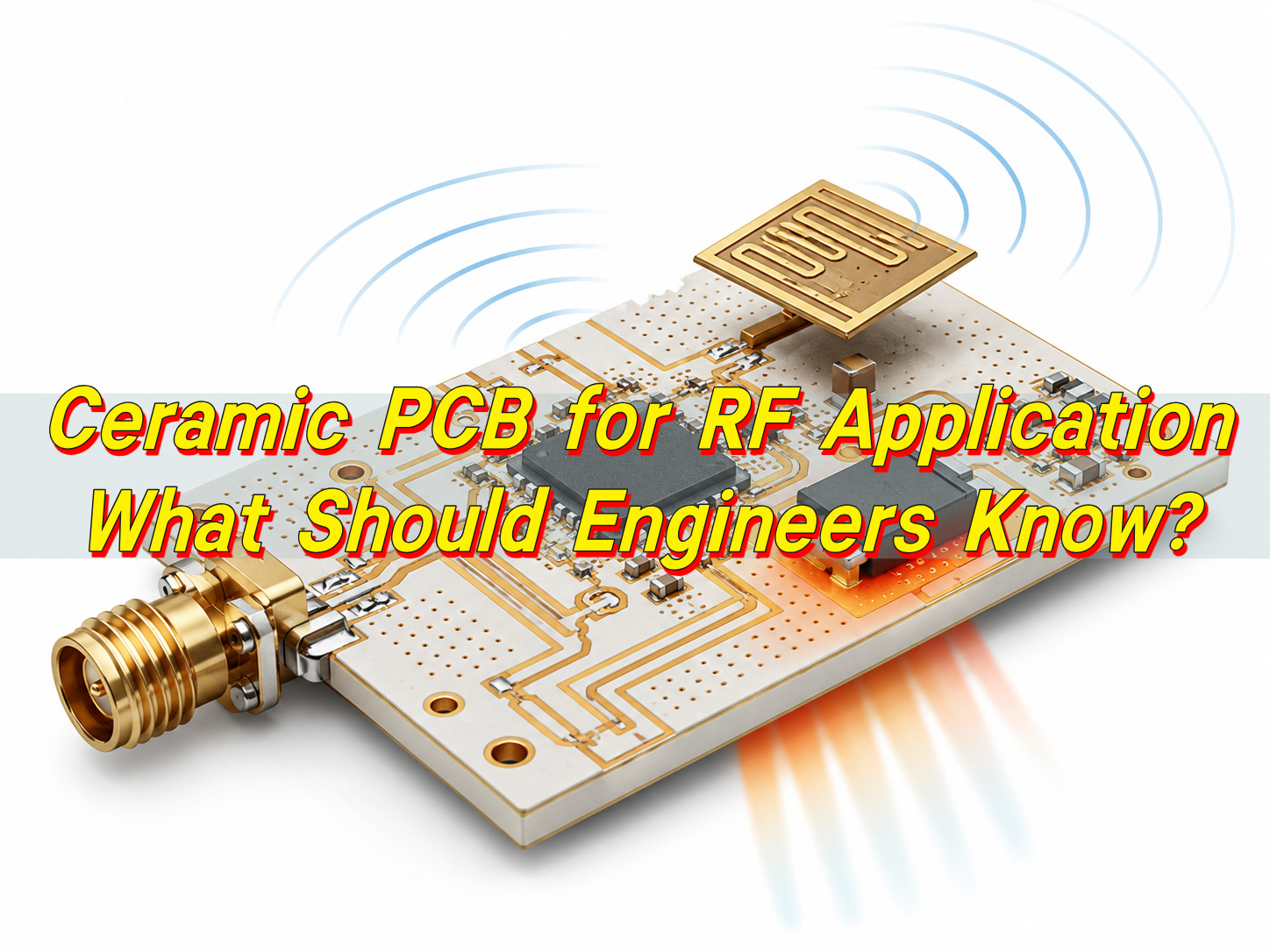
EBest Circuit (Best Technology) supports ceramic PCB fabrication for RF-related projects, including material selection, stackup review, DFM analysis, ceramic substrate processing, copper pattern control, inspection, and production support.
What Is a Ceramic PCB for RF Application?
A ceramic PCB for RF application is a printed circuit board made with a ceramic substrate instead of an organic laminate such as FR4. The ceramic layer acts as the dielectric base, while copper or other metallization forms the conductive circuit pattern. In RF designs, this substrate is selected because it provides more stable electrical and thermal behavior at higher frequencies.
For low-frequency or general digital circuits, the PCB mainly provides mechanical support and electrical connection. In RF circuits, the board also controls signal transmission. Trace width, dielectric thickness, dielectric constant, copper roughness, via structure, and ground design all influence impedance and signal loss.
Ceramic PCB technology is often used when the design needs:
- Stable dielectric behavior at high frequencies
- Lower signal loss than common FR4 materials
- Better heat dissipation around RF power devices
- Compact circuit dimensions
- High insulation strength
- Reliable performance under temperature changes
Common ceramic PCB processes include thick film, thin film, DPC, DBC, and AMB. Thin film ceramic circuits are often used for precision RF circuits, filters, attenuators, and microwave modules. DPC ceramic PCBs are suitable for fine circuit patterns, high-density layouts, and good copper bonding. DBC and AMB are more common in high-power designs where thicker copper and strong thermal transfer are required.
Why Are Ceramic PCBs Used in RF Circuits?
Ceramic PCBs are used in RF circuits because high-frequency signals are sensitive to substrate variation. At higher frequencies, even small changes in dielectric constant, material thickness, trace width, or copper surface condition can affect impedance, phase, and insertion loss.
Ceramic materials offer better dimensional and dielectric stability than many standard PCB materials. This helps RF circuits maintain more consistent performance during operation and production. For RF modules that need repeatable tuning, this stability is valuable.
Thermal performance is another major reason. RF power amplifiers, transmitters, radar modules, and microwave circuits often generate heat in small areas. If heat is not removed efficiently, device gain, frequency response, and long-term reliability may shift. Ceramic substrates, especially aluminum nitride, can move heat away from active components more effectively than FR4.
| Property | Standard FR4 | Alumina Ceramic PCB | Aluminum Nitride Ceramic PCB |
|---|---|---|---|
| Typical dielectric constant | About 4.0–4.8 | About 9.0–10.0 | About 8.5–9.0 |
| Thermal conductivity | About 0.3 W/m·K | About 20–30 W/m·K | About 140–180 W/m·K |
| Dielectric stability | Moderate | High | High |
| High-frequency loss | Higher | Lower | Lower |
| Dimensional stability | Moderate | High | High |
| Common use | General electronics | RF modules, sensors, microwave circuits | RF power modules, high-heat applications |
FR4 is still widely used in many wireless products, especially when cost is the main factor and the RF section is not highly demanding. Ceramic becomes more suitable when the design needs low loss, compact RF geometry, better heat control, or stable performance over a wide temperature range.
How Does Ceramic PCB Improve RF Signal Performance?
A ceramic PCB improves RF signal performance by creating a more stable transmission environment. In RF design, signal quality depends on impedance consistency, dielectric loss, conductor loss, grounding, and layout control. Ceramic materials help reduce several common sources of signal variation.
One key benefit is dielectric stability. The dielectric constant affects wave speed, impedance, resonant frequency, and phase behavior. If the dielectric constant changes with temperature or varies between batches, the circuit response may shift.
Another important benefit is low dielectric loss. RF signals lose energy as they move through the transmission path. Lower-loss materials help preserve signal strength, improve efficiency, and reduce unwanted heating.
Ceramic materials can also support compact design. Many ceramic substrates have a higher dielectric constant than FR4, which shortens the guided wavelength on the board. This allows certain RF structures, such as resonators, filters, and antennas, to be made smaller.
Thermal stability also supports better signal performance. RF active devices can change behavior as temperature rises. Good heat transfer helps keep the operating point more stable, which is useful for amplifiers, radar modules, and high-power communication systems.
Main RF performance benefits include:
- More consistent impedance control
- Lower dielectric loss
- Better thermal spreading
- Stable geometry during temperature cycling
- Compact RF circuit layout
- Better repeatability from prototype to production
These benefits depend on both material and manufacturing control. A ceramic substrate alone is not enough. Line width, copper thickness, via design, metallization quality, surface finish, and inspection standards must also match the RF design requirements.
What Ceramic PCB Materials Are Used for RF Applications?
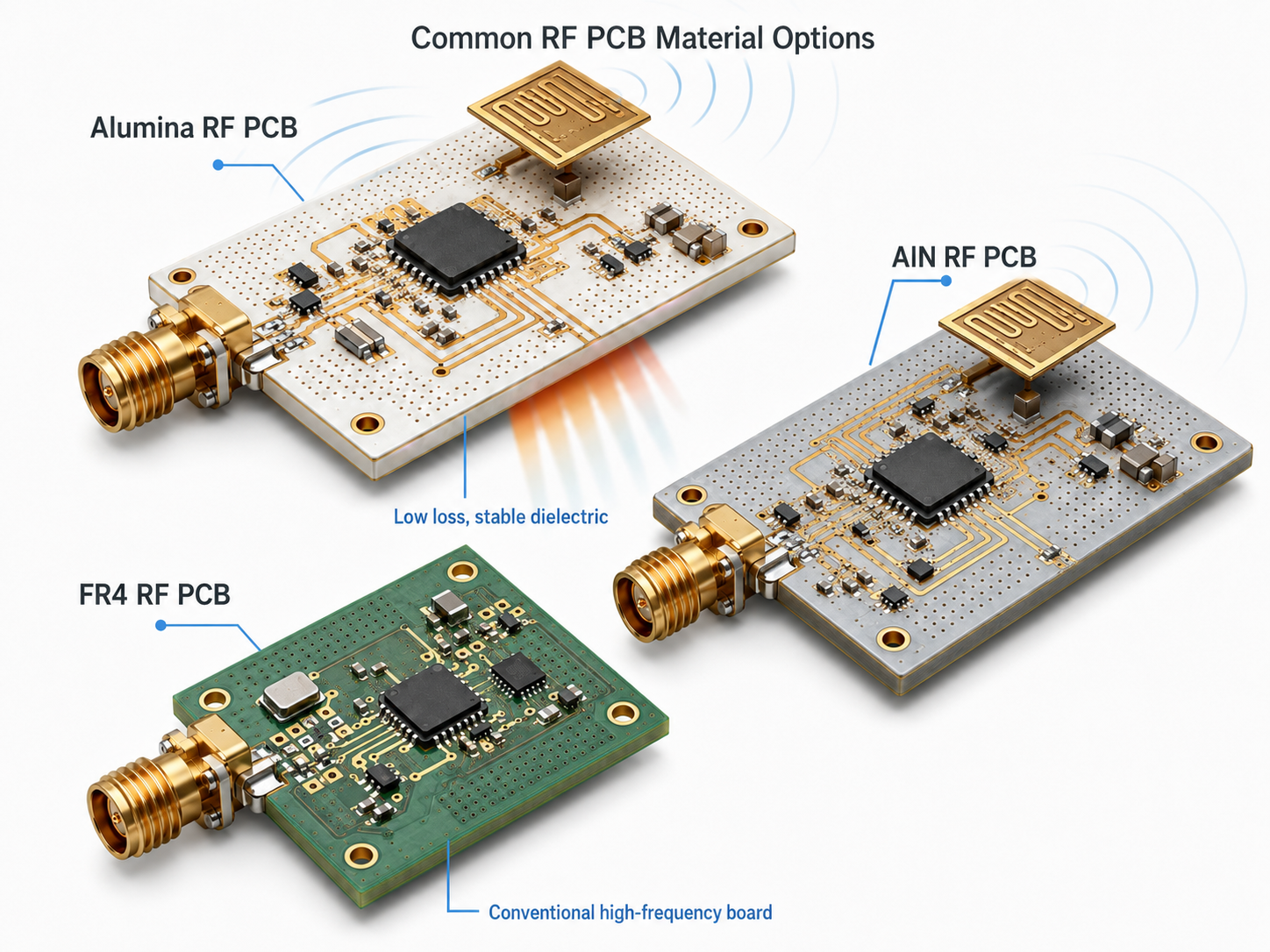
The most common ceramic PCB materials for RF applications are alumina and aluminum nitride. Other advanced ceramics may be used in specialized microwave or high-power projects, but alumina and aluminum nitride cover many practical RF design needs.
Alumina ceramic is widely used because it offers stable electrical insulation, good mechanical strength, practical cost, and reliable high-frequency behavior. It is suitable for RF modules, sensors, microwave circuits, antenna substrates, medical electronics, automotive electronics, and industrial equipment. Common grades include 96% alumina and 99.6% alumina. Higher-purity alumina is often selected when tighter stability or finer circuit features are required.
Aluminum nitride ceramic is selected when thermal performance is a priority. Its thermal conductivity is much higher than alumina, while it still provides good electrical insulation. This makes it useful for RF power amplifiers, high-power microwave modules, laser drivers, radar electronics, and compact power devices.
Specialized microwave ceramics may be used when a design needs a specific dielectric constant, low loss, or temperature coefficient. These materials are usually selected for filters, resonators, millimeter-wave modules, and other frequency-sensitive circuits.
| Material | Typical Dielectric Constant | Typical Thermal Conductivity | Main Advantage | Typical RF Use |
|---|---|---|---|---|
| 96% Alumina | Around 9.4–9.8 | About 20–25 W/m·K | Stable and cost-effective | RF modules, sensors, antenna substrates |
| 99.6% Alumina | Around 9.8–10.1 | About 25–30 W/m·K | Higher purity and tighter stability | Thin film circuits, precision RF circuits |
| Aluminum Nitride | Around 8.5–9.0 | About 140–180 W/m·K | Strong thermal conductivity | RF power modules, radar electronics |
| Microwave Ceramic | Varies | Varies | Tuned RF properties | Filters, resonators, millimeter-wave circuits |
Material selection should be made together with the manufacturing process. Thick film is suitable for robust hybrid circuits. Thin film supports fine-line precision circuits. DPC offers good copper adhesion and controlled circuit features. DBC and AMB are suitable when thicker copper and stronger thermal transfer are required.
EBest Circuit (Best Technology) can help review ceramic material options based on RF frequency, heat load, circuit density, copper thickness, and final assembly requirements.
How Does Dielectric Constant Affect RF Ceramic PCB Design?
Dielectric constant, often called Dk or εr, describes how strongly a material affects electromagnetic wave propagation. In RF ceramic PCB design, it influences impedance, wavelength, trace width, coupling, resonant frequency, and antenna size.
A higher dielectric constant shortens the wavelength on the board. This allows certain RF structures to become smaller. For example, filters, resonators, and patch antennas can often be reduced in physical size when built on a high-Dk ceramic substrate.
However, higher Dk also requires tighter design control. A small variation in Dk can shift antenna resonance or filter frequency response. Trace widths for controlled impedance may also become narrower, which increases the need for accurate fabrication.
| Design Factor | Lower Dk Material | Higher Dk Ceramic Material |
|---|---|---|
| RF structure size | Larger | More compact |
| Trace width for same impedance | Wider | Narrower |
| Signal field distribution | More field in air | More field in substrate |
| Antenna bandwidth | Often easier to widen | May become narrower |
| Resonator size | Larger | Smaller |
| Fabrication sensitivity | Moderate | Higher for fine features |
The best Dk value depends on the design target. Compact antennas and resonators may benefit from higher-Dk ceramic materials. Wider-band antennas may need careful simulation to balance size and bandwidth. RF engineers should use material data measured close to the actual operating frequency whenever possible.
For ceramic RF boards, simulation and fabrication must work together. The design model should reflect the actual substrate thickness, copper profile, dielectric constant, and process tolerance. This helps reduce tuning rounds after prototype production.
Why Is Low Loss Important in RF Ceramic PCBs?
Low loss is important because RF signal energy should reach the load, antenna, receiver, or next circuit stage with minimal attenuation. In high-frequency circuits, material loss and conductor loss can reduce signal strength, lower efficiency, and increase heat.
Dielectric loss is usually described by loss tangent or dissipation factor. A lower loss tangent means the substrate absorbs less RF energy. This is important in microwave circuits, radar systems, high-frequency communication modules, and low-noise receiver paths.
For transmitters, lower loss helps more power reach the antenna. For receivers, lower loss before amplification helps protect weak incoming signals. For filters and resonators, low loss supports cleaner frequency response and higher Q performance.
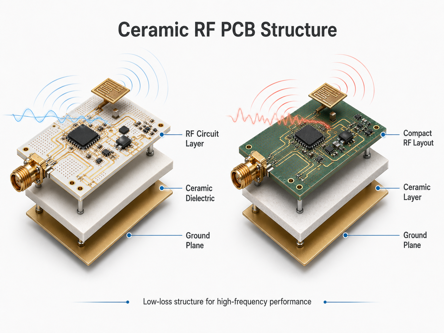
Conductor loss also matters. At high frequencies, current travels near the copper surface because of skin effect. Copper roughness, plating quality, trace width, and metallization thickness can all affect insertion loss.
| RF Design Goal | Why Low Loss Matters |
|---|---|
| Higher transmitter efficiency | More RF power reaches the output |
| Better receiver sensitivity | Weak signals lose less energy before amplification |
| Cleaner filter response | Resonant circuits maintain stronger selectivity |
| Lower operating temperature | Less signal energy becomes heat |
| Better high-frequency margin | Signal quality remains stronger as frequency increases |
| Stable module behavior | Less heat-related drift in compact circuits |
In production, low-loss performance depends on the full board structure. Material choice, copper surface, line width, solder mask, ground design, and via transitions all need review. For this reason, EBest Circuit (Best Technology) checks manufacturability details before ceramic RF PCB fabrication.
When Should You Choose Ceramic PCB Instead of FR4 for RF Applications?
Ceramic PCB should be considered instead of FR4 when the RF design requires low loss, stable dielectric behavior, better thermal conductivity, compact geometry, or high reliability in demanding environments.
FR4 remains suitable for many general electronic products. It is cost-effective, widely available, and easy to manufacture. Many low-cost wireless devices, control boards, and mixed-signal products use FR4 successfully.
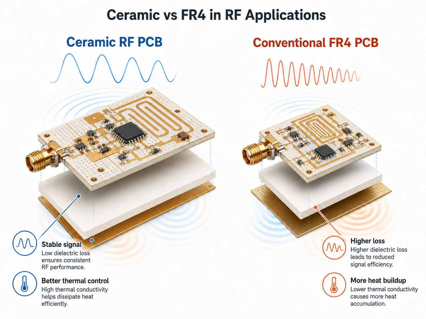
Ceramic becomes more suitable when frequency, power, temperature, or dimensional stability becomes more important. It is often used for microwave circuits, compact antennas, RF power modules, radar sensors, satellite communication circuits, and high-reliability electronics.
| Selection Factor | FR4 PCB | Ceramic PCB |
|---|---|---|
| Cost | Lower | Higher |
| Availability | Very broad | Specialized |
| High-frequency loss | Higher | Lower |
| Thermal conductivity | Low | Medium to very high |
| Dimensional stability | Moderate | High |
| Compact RF design | Limited | Stronger support |
| RF power use | Needs extra thermal design | Better natural heat path |
| Typical use | General electronics, low-cost wireless | Microwave, radar, antenna, RF power modules |
Choose ceramic when the project has one or more of these requirements:
- Operating frequency reaches microwave or millimeter-wave range
- Insertion loss must be tightly controlled
- RF power devices create concentrated heat
- Antenna or resonator size must be reduced
- The design needs stable performance across temperature changes
- The product is used in aerospace, automotive, medical, industrial, or communication equipment
In some products, a hybrid structure may be more practical. The RF section may use ceramic or another high frequency pcb substrate, while the control section uses FR4.
What RF Applications Use Ceramic PCBs?
Ceramic PCBs are used in RF applications where electrical stability, low loss, thermal control, and compact packaging are required. They are common in communication, radar, aerospace, automotive, medical, industrial, and sensing systems.
Common RF applications include:
- RF power amplifiers
- Microwave amplifier modules
- Radar sensors
- Antenna substrates
- RF filters and resonators
- Couplers and attenuators
- Satellite communication modules
- High-frequency medical equipment
- Industrial wireless sensors
- Millimeter-wave sensing modules
- High-reliability communication devices
Ceramic PCBs are also suitable for harsh-environment electronics. Aerospace and defense systems may need stable operation across wide temperature ranges. Automotive radar and industrial RF equipment often require durable substrates that support repeatable performance. Medical and communication products may need stable high-frequency behavior over long service life.
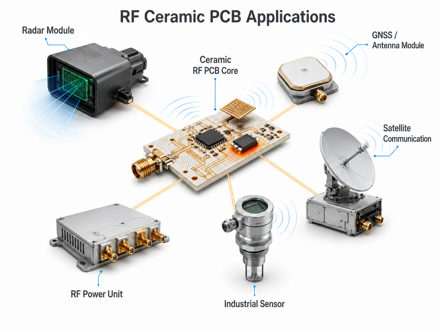
For these applications, the PCB manufacturer must control substrate quality, copper adhesion, line accuracy, hole processing, surface finish, and inspection. EBest Circuit (Best Technology) supports ceramic PCB manufacturing for RF, microwave, antenna, and power-related applications with engineering review before production.
Can Ceramic PCB Support High-Frequency Antenna Designs?
Ceramic PCB can support high-frequency antenna designs, especially when the antenna needs compact size, stable resonance, and controlled dielectric behavior. The substrate affects resonant frequency, bandwidth, impedance matching, radiation efficiency, and thermal stability.
High-Dk ceramic materials can reduce antenna size because they shorten the guided wavelength. This is useful for compact wireless modules, radar sensors, embedded antennas, and high-frequency communication devices. Ceramic substrates are often used for patch antennas, chip antennas, slot antennas, and integrated RF antenna modules.
| Design Item | Importance in Ceramic Antenna Design |
|---|---|
| Dielectric constant | Affects antenna size and resonant frequency |
| Substrate thickness | Influences impedance, bandwidth, and efficiency |
| Copper pattern accuracy | Helps keep resonance close to the target value |
| Ground structure | Affects radiation pattern and matching |
| Material loss | Influences antenna efficiency |
| Thermal performance | Supports nearby RF power components |
| Production tolerance | Improves batch-to-batch consistency |
A ceramic PCB for RF application provides a stable platform for high-frequency circuits that require low loss, controlled impedance, compact design, and better heat dissipation. It is widely used in RF modules, radar circuits, antenna substrates, microwave components, and high-power communication electronics. For projects that require reliable high frequency ceramic solutions, EBest Circuit (Best Technology) can support material review, ceramic PCB fabrication, DFM checking, inspection, and production support. Send your Gerber files, stackup, RF requirements, or project questions to sales@bestpcbs.com for an engineering review and quotation.
You may also like


Tags: ceramic PCB for RF application, high frequency circuit board, high frequency circuit materials, high frequency pcb materials, high frequency rf pcb