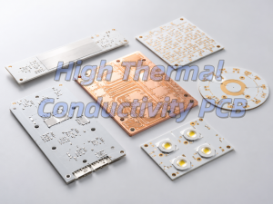
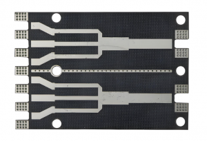
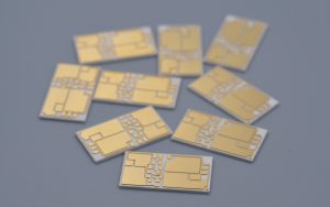
How many layers is a ceramic pcb? A ceramic PCB can have 1, 2, or multiple layers. Most designs use single-layer or double-layer structures, while complex RF, medical, or compact modules may use 4 layers, 6 layers, or more.
What Is a Ceramic PCB?
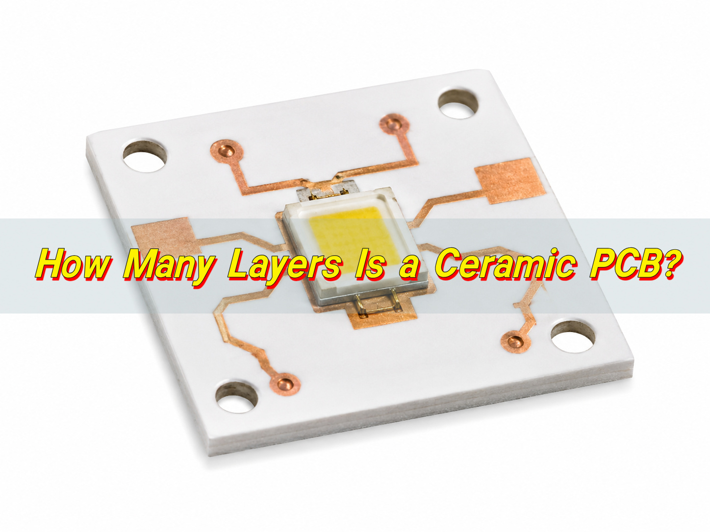
A ceramic PCB is a printed circuit board that uses a ceramic substrate as the insulating base material. Common ceramic substrates include aluminum oxide, aluminum nitride, and silicon nitride. These materials are used when the board must support heat dissipation, electrical insulation, mechanical stability, or operation at higher temperatures than standard FR4 boards can normally handle.
The substrate material affects thermal conductivity, dielectric strength, expansion behavior, copper bonding, and manufacturing process. For example, alumina is often used for general ceramic circuit boards because it offers stable insulation and reasonable cost. Aluminum nitride is selected for higher-power applications because it has much higher thermal conductivity. Silicon nitride is used in some applications that require stronger mechanical toughness and thermal cycling resistance.
Ceramic PCBs are used in LED modules, power electronics, laser devices, sensors, RF circuits, automotive modules, medical electronics, and industrial control products. These applications often require stable heat transfer from the component area to the mounting base, heat sink, or housing.
A ceramic PCB can be made as a single-layer, double-layer, or multilayer board. The layer count depends on the circuit layout, heat load, current level, signal requirements, and available board size. A simple LED carrier may only need one copper layer. A compact RF or sensor module may need several layers for signal routing, ground reference, shielding, and power distribution.
Ceramic PCB manufacturing can involve several processes, such as DPC, DBC, AMB, thick-film printing, thin-film metallization, LTCC, or HTCC. Each process has different limits for copper thickness, trace width, via structure, layer count, and cost. Because of these process differences, ceramic PCB design should be reviewed before production.
EBest Circuit (Best Technology) supports ceramic PCB projects through material selection, DFM review, PCB fabrication, component sourcing, PCBA assembly, and testing. For ceramic PCB projects, early review is important because substrate material, copper thickness, via design, surface finish, and assembly temperature all affect production feasibility.
How Many Layers Is a Ceramic PCB Usually?
A ceramic PCB usually has 1 to 6 layers in many custom manufacturing projects. Single-layer and double-layer ceramic PCBs are common in LED, power, and thermal management applications. Multilayer ceramic PCBs are used when the board requires higher routing density, ground planes, power separation, controlled impedance, or miniaturized structure.
The layer count is not decided by the ceramic material alone. It is decided by the circuit function. A circuit with only a few components and wide current paths may use one layer. A circuit with components on both sides, more routing connections, or a ground plane may use two layers. A circuit with dense ICs, RF traces, mixed signals, or compact mechanical limits may require four or more layers.
| Ceramic PCB Structure | Typical Layer Count | Common Applications | Main Design Purpose |
|---|---|---|---|
| Single-layer ceramic PCB | 1 layer | LED modules, power resistors, simple heating circuits | Direct routing and heat transfer |
| Double-layer ceramic PCB | 2 layers | Power modules, sensors, compact control boards | More routing space and backside copper options |
| Multilayer ceramic PCB | 3–8 layers | RF modules, medical electronics, industrial modules | Signal separation, power/ground layers, compact routing |
| LTCC/HTCC ceramic substrate | 6+ layers | Microwave modules, RF packages, advanced sensors | Integrated interconnects and miniaturized packaging |
For many projects, the practical layer range is limited by process, cost, and reliability requirements. Ceramic substrates are hard and dimensionally stable, but they are processed differently from FR4 laminates. More layers require tighter control of layer registration, metallization, via formation, and thermal stress.
A higher layer count can improve routing space and electrical organization, but it should have a clear design purpose. Extra layers are useful when they reduce board size, improve signal reference, support internal power distribution, or separate noisy and sensitive circuits. If the circuit is simple, extra layers may only increase cost and process risk.
Can a Ceramic PCB Be Single-Layer?
Yes, a ceramic PCB can be single-layer. This is one of the most common ceramic PCB structures. A single-layer ceramic PCB has copper traces on one side of the ceramic substrate. Components are usually mounted on the same side as the circuit pattern. Heat transfers from the component area through the ceramic substrate to the mounting base, heat sink, or system structure.
Single-layer ceramic PCBs are used when the circuit is not dense and the main requirement is heat transfer or stable insulation. Typical applications include high-power LED modules, laser diode carriers, power resistor boards, heating elements, thermal sensors, and simple power circuits. These products often require wide copper areas, stable pads, and a direct thermal path.
A single-layer design is suitable when the circuit has enough routing space on one side. It works well for layouts with fewer nets, larger components, and clear current paths. In high-current applications, trace width and copper thickness must be calculated carefully. In LED applications, the thermal pad position, solder area, and copper distribution affect heat spreading and temperature balance.
Main design points for single-layer ceramic PCBs include:
- Copper thickness: selected according to current level and thermal demand.
- Trace width and spacing: designed for current capacity, voltage clearance, and manufacturability.
- Pad design: matched to component package, soldering process, and heat transfer path.
- Substrate thickness: selected according to insulation, mechanical strength, and thermal resistance.
- Mounting method: reviewed because heat must move from the ceramic board into the final structure.
Single-layer ceramic PCBs are usually easier to inspect than multilayer designs because the circuit pattern is visible on one side. They also require fewer process steps than multilayer ceramic boards. This helps control cost when the circuit does not need additional routing layers.
For EBest Circuit (Best Technology), a typical single-layer ceramic PCB review includes substrate material, copper thickness, minimum trace/space, solder mask or protective coating, surface finish, panelization, and assembly conditions. These checks help confirm whether the single-layer structure can meet the product’s electrical and thermal requirements.
Can a Ceramic PCB Be Double-Layer?
Yes, a ceramic PCB can be double-layer. A double-layer ceramic PCB has copper circuits on both sides of the ceramic substrate. The two copper layers can be connected through vias or other ceramic-compatible interconnection methods. This structure gives more routing space than a single-layer board and allows the second side to be used for ground, power, thermal spreading, or additional signal routing.

For power electronics, backside copper can help spread heat and reduce local hot spots. For RF and sensor circuits, a continuous ground area can improve return path control and reduce coupling.
| Item | Single-Layer Ceramic PCB | Double-Layer Ceramic PCB |
|---|---|---|
| Copper layers | One side | Both sides |
| Routing space | Limited | Higher |
| Component density | Low to medium | Medium |
| Ground plane option | Limited | Easier to implement |
| Thermal spreading | Mainly through one copper side and ceramic substrate | Can use top and bottom copper areas |
| Via requirement | Usually not required | Often required |
| Manufacturing complexity | Lower | Higher |
| Typical use | LED boards, simple power circuits | Sensors, power modules, compact control boards |
Double-layer ceramic PCBs require careful via design. Via diameter, plating method, filling material, copper thickness, and ceramic thickness must match the manufacturing process. Unlike FR4, ceramic substrates are harder and more brittle, so drilling, metallization, and hole reliability require process control.
Can a Ceramic PCB Be Multilayer?
Yes, a ceramic PCB can be multilayer. A multilayer ceramic PCB has three or more conductive layers. These layers may be created through thick-film, thin-film, LTCC, HTCC, DPC-based structures, or other ceramic metallization processes. The process depends on trace resolution, layer count, via type, copper thickness, substrate material, and operating conditions.
Multilayer ceramic PCBs are used when the circuit needs compact routing, internal ground planes, power separation, shielding, or controlled signal paths. They are common in RF modules, microwave circuits, medical sensors, industrial control modules, aerospace electronics, and high-reliability compact assemblies.

A multilayer ceramic PCB is not designed in the same way as a standard multilayer FR4 PCB. Ceramic manufacturing involves different material behavior and process limits. In fired ceramic processes, shrinkage control and layer registration are important. In plated ceramic processes, via formation, copper adhesion, and thermal stress must be reviewed.
| Multilayer Ceramic PCB Type | Common Layer Range | Main Function | Typical Applications |
|---|---|---|---|
| 4-layer ceramic PCB | 4 layers | Signal, power, and ground separation | Sensors, compact control boards, RF circuits |
| 6-layer ceramic PCB | 6 layers | Higher routing density and better layer assignment | Medical electronics, RF modules, industrial modules |
| 8-layer ceramic PCB | 8 layers | More internal routing and reference planes | High-density control modules, compact power systems |
| LTCC/HTCC substrate | 6+ layers | Integrated ceramic interconnects | Microwave modules, RF packages, aerospace electronics |
A 4-layer ceramic PCB may use one or two signal layers, one ground layer, and one power or thermal layer. A 6-layer structure may provide additional routing channels or shielding layers. In RF designs, layer order and dielectric thickness affect impedance and signal behavior. In power designs, copper thickness and thermal path may be more important than the number of signal layers.
Multilayer ceramic PCBs are selected when layer function is clear. Examples include separating high-current paths from sensitive signals, adding ground reference close to RF traces, reducing board size, or integrating several functions into one ceramic module. If these functions are not needed, a single-layer or double-layer ceramic PCB may be more practical.
How Many Layers Is a PCB in Common Designs?
When engineers ask how many layers is a PCB, the answer depends on the product. Standard PCBs can be single-layer, double-layer, or multilayer. In many common electronic products, 2-layer and 4-layer FR4 boards are widely used. More complex products may use 6, 8, 10, 12, or more layers.
Simple products such as basic LED boards, low-density controllers, and low-cost consumer electronics may use one or two layers. Products with microcontrollers, connectors, power circuits, and several signal groups often use four layers. High-speed digital boards, telecom equipment, medical devices, aerospace electronics, and compact modules may require higher layer counts for routing density, impedance control, and stable power distribution.
| PCB Type | Common Layer Count | Typical Applications | Main Reason for Layer Count |
|---|---|---|---|
| Basic FR4 PCB | 1–2 layers | Simple controllers, low-density electronics | Low cost and simple routing |
| Mainstream FR4 PCB | 4 layers | Instruments, IoT devices, industrial control boards | Power/ground separation and better routing |
| Advanced FR4 PCB | 6–12 layers | Telecom, medical, industrial, high-speed systems | Dense routing and signal integrity |
| HDI PCB | 6+ layers | Compact digital products, fine-pitch IC boards | Microvias and high interconnect density |
| Ceramic PCB | 1–6 layers common | LED, power, RF, sensor, high-temperature modules | Thermal performance, insulation, material stability |
| Advanced ceramic multilayer substrate | 6+ layers | RF packages, microwave modules, compact sensors | Integrated ceramic interconnects |
A 4-layer FR4 board and a 4-layer ceramic board can have the same number of conductive layers, but their design targets are usually different. The FR4 board may be designed for general routing and cost control. The ceramic board may be designed for thermal transfer, insulation, high-frequency stability, or high-temperature operation.
What Factors Decide the Number of Ceramic PCB Layers?
The number of ceramic PCB layers is decided by circuit density, thermal demand, current level, voltage spacing, signal frequency, board size, manufacturing process, and cost target. These factors should be reviewed together because layer count affects both performance and manufacturability.
Circuit density is often the first consideration. A design with few components and simple connections may use one layer. A design with more ICs, connectors, sensors, and power nets may need two or more layers.
Thermal demand is also important. Ceramic PCBs are often selected for heat-related applications. High-power LEDs, MOSFETs, IGBTs, laser diodes, and power resistors require a planned thermal path. In these cases, copper thickness, copper area, ceramic material, and mounting method may affect performance more than layer count alone.
Current level affects copper design. High-current circuits need enough conductor width and copper thickness to control temperature rise and voltage drop. If the board area is limited, additional copper layers may help distribute current. For high-voltage circuits, creepage, clearance, substrate thickness, and insulation strength must be checked.
Signal frequency affects stack-up design. RF and microwave circuits may require controlled impedance, short return paths, continuous ground planes, and stable dielectric behavior. A multilayer ceramic PCB can provide a closer ground reference and better shielding than a single-layer board.

Board size can push the design toward more layers. If the product has enough area, a simpler layer count may work. If the board must fit into a compact housing, more layers can help maintain routing quality without increasing the footprint.
| Factor | Effect on Layer Count | Design Check |
|---|---|---|
| Component density | More components require more routing channels | Net count, package pitch, connector density |
| Heat load | Higher heat requires thermal path planning | Copper area, ceramic material, heat sink connection |
| Current level | Higher current requires more conductor capacity | Copper thickness, trace width, temperature rise |
| Voltage level | Higher voltage requires spacing control | Creepage, clearance, substrate thickness |
| Signal frequency | RF signals require controlled return paths | Stack-up, dielectric thickness, ground reference |
| Board size | Smaller boards reduce routing space | Layer assignment and component placement |
| Process capability | Manufacturing limits affect design rules | Line width, spacing, vias, registration |
| Cost target | More layers increase cost | Layer function and production value |
EBest Circuit (Best Technology) can review Gerber files, stack-up requirements, ceramic material, copper thickness, surface finish, via structure, and assembly needs before production. This review helps confirm whether the selected layer count matches the circuit and the manufacturing process.
How Does Layer Count Affect Ceramic PCB Design?
Layer count affects routing, thermal structure, electrical behavior, manufacturability, inspection, and cost. Each added layer should have a defined purpose. Common layer functions include signal routing, power distribution, ground reference, shielding, and thermal spreading.
A single-layer ceramic PCB has the most direct structure. It is suitable for circuits with low routing complexity and clear thermal requirements. The designer must place all traces on one side, so component placement and trace planning must be efficient. This structure is often used when the board carries power devices, LEDs, or heating elements with simple electrical connections.
A double-layer ceramic PCB adds routing flexibility. One side can carry components and signal traces, while the other side can support ground, power, or thermal spreading. This improves layout control and allows more compact board design. Vias become part of the reliability review because they connect both copper sides.
A multilayer ceramic PCB makes stack-up design more important. Internal layers can support ground planes, power planes, shielding, and additional routing. This is useful for RF circuits, mixed-signal modules, and compact electronics. However, multilayer ceramic designs require closer review of layer registration, via structure, copper adhesion, and thermal stress.
Layer count also affects heat movement. More layers do not automatically reduce temperature. Thermal performance depends on the ceramic material, copper thickness, copper coverage, thermal pad design, component placement, mounting surface, and heat sink connection. In some power designs, one thick copper layer on aluminum nitride may transfer heat more effectively than a multilayer stack-up with thin copper and poor mounting.
Electrical behavior changes with layer structure. A ground layer near a signal layer can improve return path control. Power and ground planes can reduce loop area and improve circuit stability. Shielding layers can help RF and mixed-signal circuits. These benefits require correct stack-up design, not only more layers.
Manufacturing cost rises with layer count. Multilayer ceramic PCBs require more processing steps, inspection, and design verification. This cost is justified when the added layers reduce board area, improve signal behavior, support power distribution, or meet mechanical constraints. If the same circuit can be built reliably with fewer layers, the simpler structure is usually preferred.
What Applications Need Multilayer Ceramic PCBs?
Multilayer ceramic PCBs are used when a product requires compact routing, stable signal behavior, high insulation, heat control, and reliable operation in a limited space. These requirements appear in RF, medical, industrial, automotive, aerospace, and advanced sensor applications.
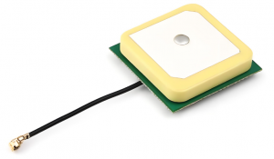
RF and microwave modules often use multilayer ceramic structures. These circuits may require controlled impedance, continuous ground reference, shielding, and stable dielectric behavior. Ceramic materials can support antenna modules, filters, radar circuits, communication modules, and microwave packages.
Medical electronics may use multilayer ceramic PCBs in compact sensor modules, diagnostic electronics, imaging-related circuits, and precision control boards. These products often require stable insulation, clean signal paths, small size, and controlled manufacturing documentation.
Industrial control products may need multilayer ceramic boards when power, sensing, and control circuits are integrated in one compact module. The stack-up can separate high-current paths from sensitive signals and provide better grounding structure.
Automotive electronics use ceramic PCB technology in LED lighting, power modules, sensors, radar systems, and control units. These products may face temperature cycling, vibration, and limited installation space. Multilayer ceramic structures are useful when routing density and electrical stability are required.
Aerospace and high-reliability electronics may use multilayer ceramic substrates for sensing, communication, radar, and control modules. These applications require stable materials, controlled process records, and reliable interconnect structures.
| Application Area | Reason for Multilayer Ceramic PCB | Design Focus |
|---|---|---|
| RF and microwave modules | Controlled impedance and compact grounding | Stack-up, dielectric control, shielding |
| Medical electronics | Small size and stable insulation | Signal quality, documentation, reliability |
| Industrial control | Integration of power, sensing, and control | Thermal path, grounding, layout separation |
| Automotive electronics | Heat resistance and compact module design | Temperature cycling, vibration, insulation |
| Aerospace electronics | Stable material behavior and process control | Traceability, reliability, registration |
| Sensor modules | Dense routing in small packages | Miniaturization, low-noise signal routing |
Multilayer ceramic PCBs are selected when single-layer or double-layer structures cannot provide enough routing space, signal control, or integration. The decision should be based on measurable design requirements, such as impedance target, board size limit, number of nets, thermal load, or grounding structure.
FAQs About Ceramic PCB Layer Count
Q1: How many layers is a ceramic PCB in most designs?
A ceramic PCB is often 1 or 2 layers in LED, power, and thermal applications. It may use 4, 6, or more layers in RF, medical, industrial, automotive, and high-reliability modules.
Q2: Can a ceramic PCB be single-layer?
Yes. A single-layer ceramic PCB has copper on one side of the ceramic substrate. It is used for high-power LED boards, laser diode carriers, heating circuits, power resistors, and other designs with simple routing and direct heat transfer requirements.
Q3: Can a ceramic PCB be double-layer?
Yes. A double-layer ceramic PCB has copper on both sides of the substrate. It is used when the design needs more routing space, backside copper, ground reference, power distribution, or a more compact layout.
Q4: Can a ceramic PCB be multilayer?
Yes. A multilayer ceramic PCB has three or more conductive layers. It may include signal layers, ground layers, power layers, shielding layers, or internal interconnect structures. It is used in RF modules, medical sensors, aerospace electronics, industrial modules, and compact control systems.
Q5: Does a higher layer count improve heat dissipation?
Not always. Heat dissipation depends on ceramic material, copper thickness, copper area, thermal pad design, board thickness, mounting method, and heat sink connection.
Q6: Can EBest Circuit help review ceramic PCB layer count?
Yes. EBest Circuit (Best Technology) can review ceramic PCB material selection, stack-up structure, copper thickness, via design, DFM requirements, fabrication process, assembly method, and testing plan. This helps confirm whether the selected layer count is suitable for production.
A ceramic PCB can be single-layer, double-layer, or multilayer. Many LED and power designs use 1 or 2 layers. RF, medical, industrial, automotive, aerospace, and compact sensor modules may use 4 layers, 6 layers, or more. The correct layer count is the one that satisfies routing, thermal, electrical, mechanical, and manufacturing requirements without adding unnecessary complexity. For ceramic PCB layer count review, stack-up support, or manufacturing consultation, contact sales@bestpcbs.com