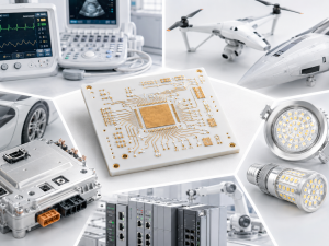
Ceramic base PCB is used when a circuit board must manage heat, electrical insulation, dimensional stability, or high-frequency performance better than a standard organic substrate. In many power, LED, RF, automotive, medical, and industrial products, the PCB is not only a carrier for components. It also becomes part of the thermal path and reliability design.
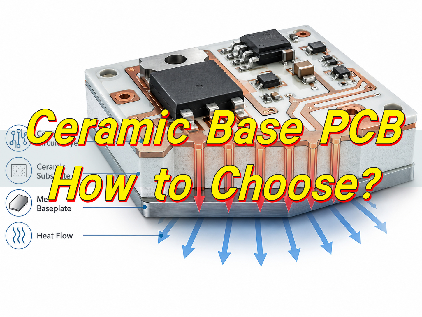
EBest Circuit (Best Technology) provides ceramic PCB fabrication, PCB manufacturing, component sourcing, PCBA assembly, DFM support, and testing for projects from prototypes to production.
What Is a Ceramic Base PCB?
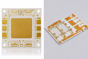
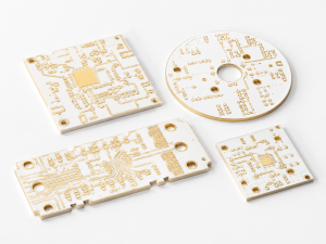
Ceramic base PCB is a printed circuit board that uses a ceramic substrate as the main insulating base. Instead of glass-reinforced epoxy, it uses materials such as alumina, aluminum nitride, silicon nitride, or other ceramic substrates. Copper circuits are formed on the ceramic surface through processes such as DPC, DBC, AMB, thick film, or thin film technology.
The ceramic base supports both mechanical and electrical functions. It carries copper traces and components, provides insulation between conductive paths, and helps transfer heat away from active devices. This is why ceramic PCB is often used in high-power and high-reliability products.
A ceramic PCB board may be single-sided, double-sided, or multilayer. Simple LED modules may only require a single-sided structure. Power modules may need thick copper and strong bonding. RF circuits may require stable dielectric properties and controlled impedance.
In sourcing, buyers may use several related terms, such as ceramic PCB board, ceramic base, or even ceramics base. The key is to confirm the actual material, copper thickness, surface finish, tolerance, operating temperature, and assembly requirements before quotation.
Ceramic base PCB is commonly used for high-power LEDs, MOSFETs, IGBTs, laser diodes, RF power amplifiers, sensors, and compact power modules. These devices often generate concentrated heat. A ceramic substrate helps move that heat from the component area to the external cooling structure.
How Is a Ceramic Base PCB Different from a Standard FR4 PCB?
Ceramic base PCB and an FR4 PCB can both carry components and copper circuits, but their substrate materials are different. FR4 uses glass fiber and epoxy resin. Ceramic PCB uses inorganic ceramic material. This difference affects thermal conductivity, temperature resistance, insulation, cost, and manufacturing method.
FR4 is suitable for many standard electronic products because it is economical, mature, and easy to process. It is widely used in consumer electronics, industrial control boards, communication products, and general PCBA projects.
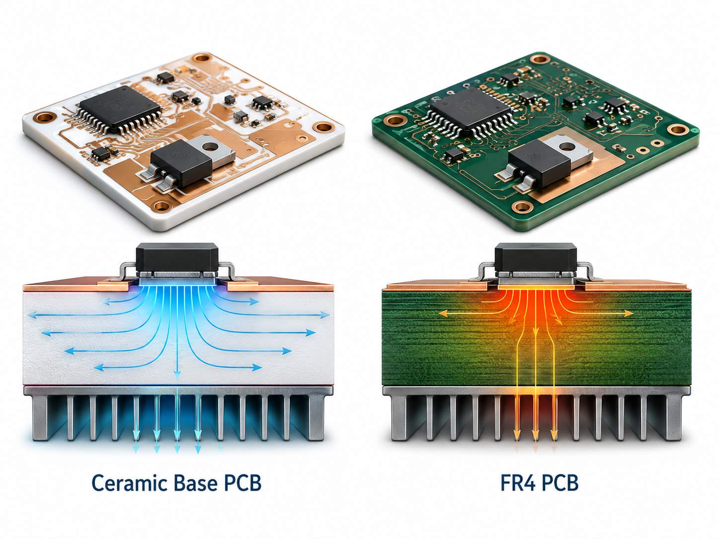
Ceramic PCB is selected when FR4 cannot meet the thermal, electrical, or environmental requirements. It is more common in power electronics, LED modules, RF circuits, semiconductor packaging, automotive electronics, and medical devices.
| Item | Ceramic Base PCB | Standard FR4 PCB |
|---|---|---|
| Base material | Alumina, aluminum nitride, silicon nitride, or other ceramic material | Glass fiber reinforced epoxy |
| Thermal conductivity | Commonly about 20–230 W/m·K, depending on material | Commonly about 0.3–0.5 W/m·K |
| Heat dissipation | Transfers heat through the ceramic substrate | Usually relies on thermal vias, copper planes, heat sinks, or metal core design |
| Temperature stability | Suitable for high-temperature environments | Suitable for general electronics |
| Electrical insulation | High dielectric strength | Good insulation for standard circuits |
| Dimensional stability | Stable under temperature change | More affected by thermal expansion and moisture |
| Processing cost | Higher | Lower |
| Typical use | Power modules, LEDs, RF circuits, sensors, automotive, medical | General electronics, control boards, digital circuits, consumer products |
The main difference is not only heat dissipation. Ceramic PCB also offers stable electrical behavior, low moisture absorption, and good mechanical stability. These features are useful when the product must work in a compact structure or demanding environment.
Manufacturing is also different. FR4 can be drilled, laminated, plated, routed, and assembled through mature PCB processes. Ceramic is harder and more brittle, so it needs controlled cutting, laser processing, metallization, copper bonding, and careful handling during assembly.
Why Are Ceramic Materials Used as a PCB Base?
Ceramic materials are used as a PCB base because they combine thermal conductivity and electrical insulation. This combination is important for circuits that must move heat away from components without creating electrical leakage or short-circuit risk.
In power electronics, heat usually comes from semiconductor devices, resistors, LEDs, or power ICs. If heat remains near the component, the product may lose efficiency, reduce output stability, or shorten service life. A ceramic base helps create a direct thermal path from the component to the substrate and then to the heat sink or housing.
Ceramic materials also maintain stable performance under high temperature. They have low moisture absorption, good chemical resistance, and reliable dimensional stability. These properties make them useful in industrial, automotive, energy, medical, and aerospace electronics.
For RF and microwave circuits, ceramic PCB materials can also provide stable dielectric properties. This helps engineers control impedance, signal loss, and phase behavior. In antennas, filters, radar modules, and RF power devices, substrate stability directly affects circuit performance.
Main reasons to use ceramic materials as a PCB base include:
- Better heat transfer than FR4
- High electrical insulation
- Stable dielectric properties
- Low moisture absorption
- Good dimensional stability
- Suitability for compact power designs
- Stable behavior under high temperature
Ceramic is not selected only because it is a premium material. It is selected when the design requires thermal, electrical, or mechanical performance that standard PCB materials cannot provide efficiently.
What Ceramic PCB Materials Are Commonly Used?
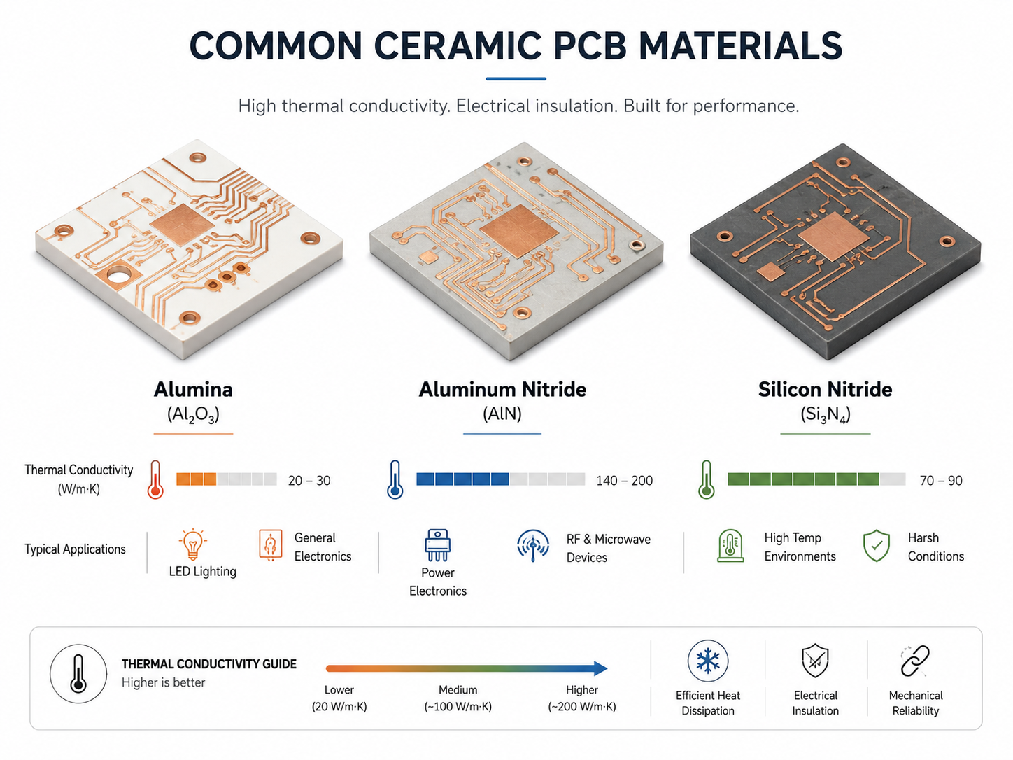
Common ceramic PCB materials include alumina, aluminum nitride, silicon nitride, and beryllium oxide. Each material has different thermal conductivity, mechanical behavior, process difficulty, and cost.
Alumina, also called Al₂O₃, is the most widely used ceramic PCB material. It offers good insulation, acceptable thermal conductivity, mature manufacturing support, and a practical ceramic board price. Common grades include 96% alumina and 99.6% alumina. For many LED, sensor, and industrial applications, alumina provides a balanced solution.
Aluminum nitride, also called AlN, is used when heat dissipation is a main requirement. It has much higher thermal conductivity than alumina and has a thermal expansion coefficient closer to silicon. This makes it suitable for high-power LEDs, laser modules, semiconductor packages, and compact power modules.
Silicon nitride, or Si₃N₄, is known for mechanical strength and thermal shock resistance. It is often used in automotive power modules and reliability-focused power electronics. It is useful when the design must handle temperature cycling, vibration, or mechanical stress.
Beryllium oxide, or BeO, has high thermal conductivity, but it requires strict safety control during processing. Because of handling concerns, many projects use aluminum nitride as an alternative when high thermal conductivity is required.
| Material | Typical Thermal Conductivity | Main Features | Common Applications |
|---|---|---|---|
| Alumina / Al₂O₃ | About 20–30 W/m·K | Mature process, good insulation, controlled cost | LEDs, sensors, industrial electronics, general ceramic PCB |
| Aluminum Nitride / AlN | About 170–230 W/m·K | High thermal conductivity, good semiconductor compatibility | High-power LEDs, laser modules, power modules |
| Silicon Nitride / Si₃N₄ | About 60–90 W/m·K depending on grade | High mechanical strength, thermal shock resistance | Automotive power electronics, high-reliability modules |
| Beryllium Oxide / BeO | About 200–300 W/m·K | High thermal conductivity, special handling requirements | Specialized RF and power applications |
Material selection should match the working conditions. Alumina is often suitable for cost-sensitive applications with moderate heat. Aluminum nitride is used when thermal conductivity is critical. Silicon nitride is useful when mechanical reliability is a priority.
A reliable ceramic base PCB manufacturer should not recommend material based only on performance data. It should also consider cost, manufacturability, lead time, copper structure, surface finish, and assembly method.
How Does a Ceramic Base PCB Help with Heat Dissipation?
A ceramic base PCB helps with heat dissipation by forming a shorter and more efficient thermal path between heat-generating components and the external cooling structure. Heat can move from the component pad into the copper layer, through the ceramic substrate, and then into the heat sink, metal housing, or thermal interface material.
In a standard FR4 PCB, heat transfer through the substrate is limited. Engineers often add thermal vias, large copper planes, heat sinks, or metal core structures to improve thermal performance. These methods can work well, but they may require more board space and more design control.
Ceramic substrates have higher thermal conductivity, so they can transfer heat more directly through the board. This is useful in compact power circuits where heat is concentrated in a small area.
| Substrate Type | Typical Thermal Conductivity | Design Meaning |
|---|---|---|
| FR4 | About 0.3–0.5 W/m·K | Suitable for general circuits; needs additional thermal design for higher power |
| Aluminum PCB dielectric layer | Often about 1–3 W/m·K | Useful for LED and power boards, but dielectric layer affects heat transfer |
| Alumina ceramic | About 20–30 W/m·K | Suitable for moderate to high thermal needs |
| Aluminum nitride ceramic | About 170–230 W/m·K | Suitable for high-power and compact thermal designs |
| Silicon nitride ceramic | About 60–90 W/m·K depending on grade | Suitable when heat transfer and mechanical strength are both important |
Copper thickness also affects thermal behavior. Thick copper helps spread heat across the surface. Ceramic helps conduct heat through the substrate. When these two functions are combined properly, the PCB can support higher power density.
Substrate thickness should also be reviewed. A thinner ceramic substrate can reduce thermal resistance, but it must still meet insulation and mechanical strength requirements. A thicker substrate may improve handling strength, but it can increase the thermal path length.
For LED modules, ceramic PCB helps control junction temperature. This supports stable brightness, color performance, and operating life. For power semiconductors, better heat transfer helps reduce thermal stress and improves operating stability.
What Are the Main Benefits of Ceramic Base PCBs?
Ceramic base PCBs provide thermal, electrical, and mechanical advantages for applications that require more than standard PCB performance. Their main value is the ability to conduct heat while maintaining insulation.
The first benefit is thermal conductivity. Ceramic substrates transfer heat more efficiently than FR4. This helps high-power components work within a more controlled temperature range.
The second benefit is electrical insulation. Ceramic materials can provide high dielectric strength while still allowing heat to pass through the substrate. This is useful for power modules, LED arrays, high-voltage circuits, and compact electronics.
The third benefit is dimensional stability. Ceramic substrates expand less than many organic materials under temperature change. This helps maintain circuit accuracy and solder joint stability.
The fourth benefit is environmental stability. Ceramic materials have low moisture absorption and good resistance to many chemicals. This is useful in industrial, automotive, medical, and outdoor applications.
Main benefits include:
- High thermal conductivity for power-dense designs
- Good electrical insulation for high-voltage circuits
- Stable size under temperature change
- Low moisture absorption
- Suitable for high-temperature environments
- Good compatibility with compact modules
- Stable dielectric behavior for RF designs
Ceramic base PCB is especially useful when thermal management, insulation, and reliability must be handled in the same structure. It can also reduce dependence on large external cooling designs when the product structure allows a direct thermal path.
What Applications Use Ceramic Base PCBs?
Ceramic base PCBs are used in products that require heat dissipation, insulation, compact size, stable signal behavior, or long-term reliability. They are common in LED lighting, power electronics, RF modules, automotive electronics, medical devices, aerospace systems, and sensor modules.
| Application Area | Common Use | Why Ceramic Is Used |
|---|---|---|
| LED lighting | High-power LED, UV LED, automotive lighting | Heat dissipation and compact structure |
| Power electronics | Inverters, converters, MOSFET and IGBT modules | Thermal transfer and insulation |
| RF and microwave | Antennas, filters, radar modules, amplifiers | Stable dielectric properties |
| Automotive | EV power units, lighting, sensors | Thermal cycling and reliability |
| Medical electronics | Sensors, imaging modules, compact power circuits | Stability and process control |
| Aerospace and UAV | RF modules, power control, sensors | Weight, heat, and reliability considerations |
EBest Circuit (Best Technology) supports ceramic PCB projects for customers in lighting, industrial control, communication, medical, automotive, and power electronics fields. For these projects, early review of material, copper thickness, thermal path, and assembly method helps improve manufacturability.
How Is a Ceramic Base PCB Manufactured?
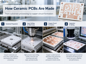
Ceramic base PCB manufacturing depends on the substrate material and copper formation process. The main production steps include ceramic substrate preparation, cleaning, metallization, copper formation, circuit patterning, surface finishing, inspection, and profiling.
The process starts with ceramic substrate selection. The factory checks material type, thickness, flatness, surface quality, and dimensional tolerance. A clean and stable surface is important because copper adhesion depends on the substrate condition.
The next step is copper formation or metallization. Different methods are used depending on the design requirement.
DPC, or Direct Plated Copper, uses sputtering and electroplating to form copper on ceramic. It is suitable for fine lines, compact layouts, and precise circuit structures.
DBC, or Direct Bonded Copper, bonds copper foil directly to ceramic at high temperature. It is often used for power electronics because it supports thick copper and higher current capacity.
AMB, or Active Metal Brazing, uses active brazing material to bond copper and ceramic. It is used for high-reliability power modules that require strong bonding.
Thick film technology prints conductive paste on ceramic and fires it at high temperature. It is often used in hybrid circuits and ceramic electronic modules.
Thin film technology forms very fine and accurate circuit patterns. It is suitable for precision applications where tight feature control is required.
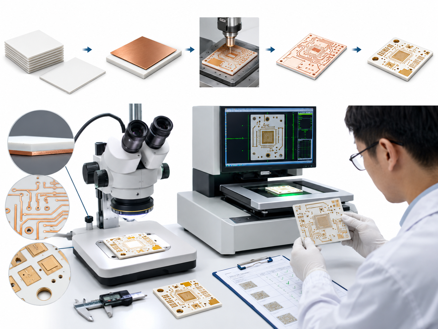
A typical process flow includes:
- Ceramic substrate inspection
- Surface cleaning and preparation
- Copper bonding or metallization
- Circuit imaging and etching
- Plating and surface finish
- Laser cutting, drilling, or profiling
- Electrical testing and visual inspection
- Dimensional and surface quality check
Design rules vary by process. DPC can support finer features, while DBC is better for thick copper and high-current designs. AMB is selected when bonding strength and reliability are important. The correct process should be chosen based on copper thickness, line width, current load, thermal requirement, and cost target.
What Affects Ceramic PCB Cost?
Ceramic PCB cost is affected by material type, substrate size, ceramic thickness, copper thickness, circuit complexity, surface finish, process type, tolerance, testing, quantity, and assembly requirements. When evaluating ceramic board price, the complete specification is more important than board size alone.
Material is a major factor. Alumina is usually more cost-effective and suitable for many standard ceramic PCB applications. Aluminum nitride costs more because it provides much higher thermal conductivity and requires more controlled processing. Silicon nitride may also cost more due to its mechanical properties and specialized applications.
Copper thickness affects both material usage and process difficulty. Thick copper supports higher current and better heat spreading, but it requires more process control during bonding, etching, and inspection.
Circuit complexity also affects cost. Fine lines, tight spacing, small holes, special shapes, and tight tolerances require more precise production. Surface finish can also change cost, especially when the design requires ENIG, silver, gold, or wire-bondable finishes.
| Cost Factor | Effect on Price | Practical Note |
|---|---|---|
| Ceramic material | AlN and Si₃N₄ usually cost more than alumina | Select material based on actual thermal and mechanical needs |
| Substrate thickness | Non-standard thickness may increase cost | Use standard thickness when possible |
| Copper thickness | Thick copper increases material and process cost | Match copper to current and heat requirements |
| Process type | DPC, DBC, AMB, thick film, and thin film have different cost levels | Choose process based on performance and manufacturability |
| Circuit complexity | Fine features and tight tolerances increase production difficulty | Keep layout practical for the selected process |
| Surface finish | Special finishes add cost | Define soldering or bonding requirements clearly |
| Quantity | Small batches have higher unit cost | Use prototypes for validation, then optimize batch production |
| Testing and documentation | Extra inspection increases cost but improves control | Specify only required test items |
To control ceramic PCB cost, avoid unnecessary over-specification. For example, aluminum nitride may not be required if alumina already meets the thermal target. Very thick copper may not be useful if the current load is moderate. A DFM review can help identify these issues before production.
EBest Circuit (Best Technology) can review ceramic PCB designs before manufacturing. This helps confirm material selection, copper structure, surface finish, panel use, and assembly feasibility. For ceramic PCB projects, early engineering review can improve cost control and production stability.
How Do You Choose a Reliable Ceramic Base PCB Factory?
To choose a reliable ceramic base PCB factory, evaluate its material knowledge, process capability, DFM support, inspection system, traceability, PCBA support, and communication quality. Ceramic PCB production is more specialized than standard FR4 PCB fabrication, so the supplier should understand the design purpose, not only the Gerber files.
First, check material capability. A qualified ceramic base PCB manufacturer should understand alumina, aluminum nitride, silicon nitride, copper thickness options, substrate thickness, thermal conductivity, dielectric properties, and surface finish choices. The supplier should help match the material to heat, voltage, mechanical stress, frequency, and budget.
Second, check process capability. Confirm whether the factory supports DPC, DBC, AMB, thick film, thin film, or the specific ceramic process required by your design. Also check minimum trace and spacing, copper thickness range, hole processing, outline tolerance, and available surface finishes.
Third, check engineering support. Ceramic PCB often needs DFM review before production. The factory should review copper-to-edge spacing, pad design, thermal path, substrate thickness, panelization, soldering method, and assembly handling.
Fourth, check quality control. Useful inspection items include electrical testing, visual inspection, dimensional measurement, copper thickness measurement, adhesion testing, surface finish inspection, and material traceability. For medical, automotive, industrial, or aerospace products, documentation control is also important.
| Selection Point | What to Check |
|---|---|
| Material knowledge | Alumina, AlN, Si₃N₄, substrate thickness, thermal conductivity |
| Process capability | DPC, DBC, AMB, thick film, thin film, copper thickness |
| DFM support | Layout review, thermal path review, pad design, manufacturability |
| Quality control | E-test, dimensional inspection, adhesion check, surface finish control |
| Traceability | Material batch, process records, inspection data |
| PCBA support | SMT assembly, component sourcing, testing, fixture support |
| Communication | Clear quotation, technical feedback, delivery updates |
EBest Circuit (Best Technology) supports ceramic PCB fabrication, PCB manufacturing, component sourcing, SMT assembly, testing, and one-stop PCBA production. This is useful when the ceramic PCB is part of a complete module and requires coordination between bare board fabrication and assembly.
Before requesting a quotation, prepare Gerber files, drill files, outline drawings, material requirements, substrate thickness, copper thickness, surface finish, quantity, operating temperature, voltage, current load, thermal target, and assembly notes. If the material has not been finalized, provide the application background so the factory can recommend a practical option.
To summarize, ceramic base PCB is suitable for designs that require better heat dissipation, electrical insulation, dimensional stability, and reliability than standard FR4 can provide. Alumina is often used for balanced cost and performance, aluminum nitride is used for high thermal conductivity, and silicon nitride is suitable for mechanically demanding applications. For ceramic base PCB fabrication, ceramic PCB board manufacturing, or PCBA project support, contact EBest Circuit (Best Technology) at sales@bestpcbs.com for quotation and engineering review.