PCB manufacturing PCB manufacturing
Home > Blog

PCB Bare Board Testing: Methods, Standards, Reports & Acceptance Criteria

July 20th, 2026

PCB bare board testing verifies opens and shorts before assembly. It compares the electrical networks of an unpopulated printed circuit board with approved connectivity data before defects become harder and more expensive to isolate. A meaningful result must also identify the tested revision, coverage, limits, exclusions, traceability, and disposition rules.

A “passed” label is meaningful only when the method, source netlist, limits, exclusions, and report content are defined. Electrical verification does not replace visual, dimensional, impedance, cleanliness, solderability, or reliability controls.

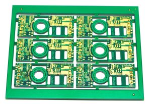
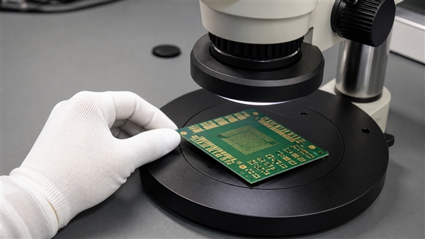
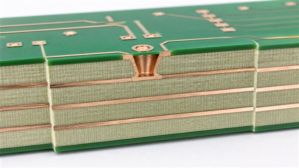
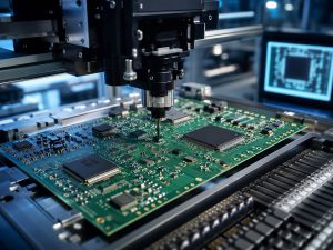
Flying probes performing PCB bare board testing on an unpopulated circuit board

What Is PCB Bare Board Testing?

PCB bare board testing verifies continuity and isolation. Continuity testing and isolation testing compare accessible conductive points with a reference derived from the released design. Net count, board density, via structures, access constraints, and special measurements determine test complexity.

The test is often called bare-board electrical test, E-test, continuity-and-isolation test, or netlist test. It can identify electrical opens and shorts, but it does not prove that every physical feature meets drawing requirements. It also does not guarantee that an assembled product will function. Visual workmanship, dimensions, copper and plating requirements, controlled impedance, solderability, cleanliness, and assembly performance remain separate verification activities.

Why Is Bare Board Testing Important Before PCB Assembly?

PCB bare board testing prevents known defects from entering assembly. Its value can be divided into four practical benefits:

  • Lower assembly loss: Detecting opens and shorts before component placement avoids wasting components, reflow capacity, inspection time, and troubleshooting labor.
  • Earlier defect containment: Testing close to PCB fabrication allows affected boards to be isolated before more value is added. This is especially useful for fine-pitch parts, buried connections, dense multilayers, and products that are difficult to probe after assembly.
  • Clear responsibility boundary: The PCB manufacturer can document the electrical condition at shipment, while the assembler controls handling, storage, assembly, and downstream testing.
  • Better purchase-order control: Defined coverage reduces disputes caused by vague language such as “electrically tested.” The order should identify the data revision, coverage level, acceptance basis, reporting needs, and special test conditions.

What Defects Can Bare Board Testing Detect?

PCB bare board testing finds electrical connectivity defects. The main results depend on test access, the approved program, and the specified measurement conditions:

  • Open circuits: PCB bare board testing detects interrupted nets caused by incomplete etching, cracked copper, failed via connections, annular-ring breakout, poor hole-wall metallization, or routing damage.
  • Short circuits: It detects unintended connections caused by copper bridges, conductive residue, imaging errors, plating anomalies, or incorrect fabrication data.
  • Intermittent connections: Unstable defects may require repeated measurements, thermal conditioning, resistance monitoring, microsectioning, or reliability testing.
  • Not covered by electrical testing: Visual defects, dimensional errors, impedance deviations, contamination, solder-mask registration, and material conditions require separate inspection or measurement.

Flying Probe vs Fixture Testing: Which Bare Board Testing Method Should You Choose?

For PCB bare board testing, use flying probe testing for flexibility. Use fixture testing for throughput. The final choice depends on volume, revision stability, access, setup cost, and required test time.

Decision Factor Flying Probe Fixture Testing
Operating principle Moving probes contact test points sequentially according to the test program A dedicated adapter contacts many test points in parallel
Typical fit Prototype, low volume, frequent revision Stable design, medium-to-high volume
Dedicated tooling Usually not required Required and revision-specific
Setup profile Program generation and validation Fixture plus program generation and validation
Throughput Sequential probing; often slower Parallel contact; often faster after setup
Upfront cost Lower because no dedicated fixture is normally needed Higher because the fixture must be designed, built, and validated
Cost per board Can remain higher as test time increases with point count Can decrease across stable production volumes after setup
Revision response Program changes may be sufficient Fixture rework or replacement may be needed
Access risk Probe reach, pad size, stability, and routing Probe density, fixture mechanics, alignment, and wear
Board support Requires stable positioning during probe movement Requires uniform support and controlled pressure across the fixture
Maintenance Probe condition, alignment, and program control Probe wear, fixture cleaning, storage, alignment, and revision control
Special measurements Flexible for selected points, low-resistance checks, or engineering investigation when equipment supports them Suitable for repeatable production measurements when designed into the fixture and switching system
Primary limitation Runtime increases with test-point count and measurement scope Tooling cost and lead time are difficult to justify for changing designs
Best selection rule Choose when flexibility and low setup commitment outweigh runtime Choose when stable volume and throughput justify dedicated tooling
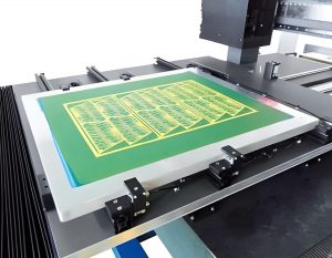
Bare PCB positioned on a dedicated bed-of-nails electrical test fixture

Which Board and Order Factors Affect Test-Method Selection?

Balance coverage risk, design stability, setup cost, and runtime. Review production quantity, expected repeat orders, board size, net and test-point count, pad geometry, layer count, via technology, panel format, and required measurements. A prototype likely to change favors flexible programming; a mature design produced repeatedly may justify a fixture whose preparation cost is distributed across more units.

Then examine what must be tested and what is physically accessible. Fine-pitch pads, solder-mask clearance, surface finish, board support, bow and twist, and probe force can affect contact reliability. Controlled-impedance verification, very low resistance, or elevated-voltage isolation may require methods beyond a basic continuity-and-isolation routine. The manufacturer should review unusual requirements before quotation so the chosen method, limits, tooling, report, and lead time are aligned.

How Does the PCB Bare Board Testing Process Work?

PCB bare board testing starts with controlled data. Confirm the released revision, reference netlist, accessible points, and approved limits before loading the board. The following eight steps create a traceable test and release process.

  1. Review the order and data package. Confirm part number, revision, quantity, panelization, applicable drawings, test coverage, special nets, reporting, and acceptance requirements.
  2. Create and compare the test reference. Generate connectivity from trusted design data and perform an independent comparison where required to reduce the risk of testing a fabrication error against the same erroneous source.
  3. Prepare the program and access plan. Map test points, choose probe paths or fixture contacts, apply agreed limits, and identify intentionally untested or inaccessible points.
  4. Validate setup. Check alignment, contact, board support, program revision, fixture identification, and known-reference behavior before production testing.
  5. Run continuity and isolation checks. Test the required networks and capture failures with sufficient location information for diagnosis.
  6. Confirm suspect results. Clean or inspect contact surfaces, repeat the measurement under controlled rules, and distinguish contact instability from a repeatable board defect.
  7. Control nonconforming boards. Segregate failures, record disposition, control any repair or retest authorization, and preserve traceability.
  8. Release records. Link the test status and report to the correct lot, date, equipment or program, and approved product revision.

Which Standards Apply to PCB Bare Board Testing?

PCB bare board testing standards must be named by revision. IPC-9252B addresses test data, parameters, equipment, and fixturing for unpopulated boards. IPC’s current revision table marks IPC-9252 as no longer maintained. The purchase order should therefore identify the accepted revision or an agreed alternative. Its scope is conductive-network verification, not every physical, material, dimensional, or assembly requirement.

IPC-A-600 addresses externally and internally observable acceptability conditions; IPC’s revision table listed IPC-A-600M in May 2025. The applicable IPC-6010-series performance specification and procurement documentation define requirements for the relevant board type and class. Drawings, purchase orders, approved deviations, and sector-specific requirements may add controls, so the contract should state document revisions and order of precedence.

High-voltage, aerospace, medical, automotive, or other high-reliability applications may demand additional validation, records, or process controls. Those requirements should be specified by the responsible design authority. A supplier should not infer a hipot voltage, insulation criterion, test class, or sampling permission from the product description alone.

What Files Are Needed for PCB Bare Board Testing?

The test package must identify the product and test reference. Provide the following controlled files and instructions:

  • Fabrication data: Supply the released Gerber or ODB++ package with clear layer identification.
  • Drill data: Include plated and non-plated drill files plus any required drill drawing or tool information.
  • Product identification: State the part number, fabrication revision, board or panel drawing, quantity, and panelization requirements.
  • Reference netlist: Provide IPC-D-356 or trusted CAD-derived connectivity data when an independent electrical reference is required. If the netlist is extracted from fabrication files, define how it is generated and compared.
  • Test requirements: Define coverage, continuity and isolation limits, inaccessible points, no-probe areas, and any special measurement conditions.
  • Special structures: Identify net ties, intentionally connected planes, embedded components, isolated copper, edge contacts, castellations, coupons, and controlled-impedance requirements.
  • Reporting instructions: Specify lot- or serial-level reporting and whether the deliverable must include a certificate, summary, raw measurements, or failure map.
  • Data-control rules: Define secure transfer, authorized access, retention, and deletion requirements for commercially sensitive design files.

100% Netlist Testing vs Optimized Testing vs Sampling

These three coverage models are not interchangeable. The order must define the tested units, program scope, exclusions, and approval basis rather than relying on a short coverage label.

Coverage Model Meaning to Confirm Procurement Control
100% netlist test Every production board runs the defined electrical program; this does not mean every physical feature is measured Define accessible nodes, program scope, exclusions, and lot traceability
Optimized test The program reduces redundant contacts or sequences while preserving the agreed network verification Approve the optimization basis, retained coverage, and excluded points
Sampling Only units selected by the approved sampling plan are tested; other boards remain untested State the sample size, selection method, acceptance rule, risk basis, and authorization

Sampling must not replace contracted every-board testing. Any change requires written authorization under the applicable specification and risk assessment.

What Are the Acceptance Criteria for Bare PCB Testing?

Acceptance criteria must turn “pass” into measurable rules. Define the following items before program approval and production testing:

  • Continuity limit: State the maximum permitted resistance for an intended net, using values appropriate to trace length, conductor geometry, connectors, planes, and low-resistance paths.
  • Isolation limit: Define the minimum resistance or maximum leakage allowed between separate nets. High-voltage products may require different limits and test conditions from routine circuitry.
  • Coverage: Specify whether every board, an optimized net set, or an approved sample is tested. Identify inaccessible points, excluded features, and permitted optimization.
  • Special measurements: For hipot, four-wire resistance, or other special checks, define voltage, current, dwell time, temperature, measurement method, test location, and guarding requirements.
  • Data identity: Link acceptance to the correct part number, fabrication revision, controlled netlist or checksum, test-program revision, and approved change record.
  • Failure confirmation: Define how contact instability is distinguished from a repeatable board defect and which controlled measurements may be repeated.
  • Repair and retest: State whether repair is permitted, who can authorize it, which workmanship rules apply, and whether the affected net or complete program must be rerun.
  • Required evidence: Define the certificate, test summary, failure map, raw results, traceability fields, and record-retention period required for acceptance.

Do not apply one generic limit to every design. Electrical limits must follow the product’s design intent, governing specification, and confirmed test feasibility.

What Should a Bare Board Test Report Include?

A useful report must link results to the delivered boards. Specify the required report level in the purchase order:

  • Product identity: Customer part number, fabrication revision, lot or work order, and panel or serial identification when required.
  • Test quantity: Quantity received, tested, passed, failed, repaired, retested, and finally released.
  • Coverage: Every-board, optimized, or sampling status plus inaccessible points and approved exclusions.
  • Test method: Flying probe, fixture, or other approved method, including program and fixture identification.
  • Acceptance settings: Continuity and isolation limits plus voltage, current, dwell time, or other special conditions when applicable.
  • Equipment control: Tester identification and calibration-status reference when contractually required.
  • Failure history: First-pass failures, confirmed defects, retest results, repair status, and final disposition.
  • Authorization: Test date, operator or approval record, applicable specification, and acceptance basis.
  • Record control: Report format, lot or serial linkage, retention period, and retrieval requirements.

A certificate is not the same as a detailed test report. Name the exact deliverable required before production begins.

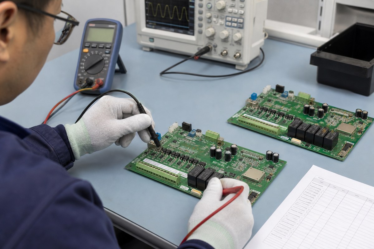
Quality engineer reviewing a bare PCB and electrical test results

What Causes False Failures in Bare Board Testing?

False failures usually come from contact, setup, or data errors. False failures in flying probe testing and fixture testing should be checked before a board is classified as defective:

  • Contaminated contact surfaces: Oxidation, residue, debris, or surface-finish variation can increase or destabilize contact resistance.
  • Restricted probe access: Small pads, solder-mask encroachment, or unsuitable no-probe geometry can prevent reliable contact.
  • Probe condition: Worn, dirty, damaged, or incorrectly selected probes can produce unstable readings.
  • Force and alignment: Incorrect probe force, fixture alignment, fiducial recognition, or board positioning can move contact away from the target.
  • Board support: Bow, twist, movement, or inadequate support can prevent uniform fixture contact or allow a thin board to flex.
  • Incorrect test data: A Gerber and netlist revision mismatch, wrong layer polarity, misunderstood net tie, isolated-copper definition, or incorrect drill file can create systematic false failures.
  • Fixture or program control: Worn fixture contacts, an unvalidated program change, or mismatched fixture identification can affect repeated production tests.

Preserve the original result before retesting. Correct only a verified contact or setup issue, rerun the defined scope, and record both outcomes.

How Should Failed Boards and Retests Be Controlled?

Confirmed failures must be segregated and traceable. The record should retain board or panel identity, failed net or point information, failure type, test program, date, and investigation status. This prevents accidental mixing and gives process engineering enough evidence to search for recurring patterns across panel position, layer, drill tool, plating batch, or routing operation.

Retest rules should distinguish contact confirmation from a disposition-changing retest. Cleaning a pad and repeating an unstable contact may be legitimate when the original result is retained. A repeatable open or short requires nonconformance control. Permitted repairs need authorization, workmanship criteria, inspection, retesting of the complete affected scope, and traceability. Authorized personnel must approve scrap, use-as-is, or deviation decisions.

What Affects PCB Bare Board Testing Cost and Lead Time?

Cost and lead time depend on setup, runtime, and reporting. The main drivers are:

  • Order quantity: Low volumes often favor flying probe; stable repeated volumes may justify dedicated fixture cost.
  • Net and point count: More nodes, dense access, and complex connectivity increase programming and test time.
  • Board and panel format: Large panels, thin boards, unusual outlines, and difficult support conditions can require additional handling or tooling.
  • Test method: Flying probe reduces dedicated tooling but may increase runtime; fixture testing adds preparation cost but improves throughput after validation.
  • Revision stability: Design or panel changes may require program revalidation, fixture modification, or replacement.
  • Special measurements: Hipot, four-wire resistance, controlled-impedance reporting, or custom limits may require engineering review and additional setup.
  • Traceability and reports: Serial-level records, raw measurements, failure maps, or customized reports add data-handling and review time.
  • Input completeness: Missing files, conflicting revisions, undefined limits, or late requirement changes delay program approval and quotation.

Release a complete, stable test package at quotation. This is the most effective way to reduce avoidable setup cost and schedule delay.

PCB Bare Board Testing Checklist

Resolve coverage and reporting decisions before order release. This PCB bare board testing checklist captures the requirements that materially change risk, documentation, or delivery. Not every item applies to every PCB, but each omission should be a deliberate engineering or procurement decision rather than an assumption.

  • Product identity: Confirm the customer part number, fabrication revision, and approved data set.
  • Coverage model: State whether every board, an optimized net set, or a defined sample is tested.
  • Test method: Identify the required method or allow the manufacturer to propose flying probe or fixture testing.
  • Electrical limits: Define continuity, isolation, and any special measurement conditions.
  • Reference netlist: Provide an independent netlist when required and define how data comparison is controlled.
  • Special structures: Identify net ties, embedded parts, isolated copper, coupons, edge contacts, and no-probe areas.
  • Physical access: Confirm test access, solder-mask clearance, surface finish, support, and warp expectations.
  • Applicable documents: Name the governing standards, revisions, performance class, drawings, and order of precedence.
  • Failure control: Define failure confirmation, repair authorization, retest scope, and nonconformance reporting.
  • Traceability: Specify lot, panel, or serial traceability and record-retention period.
  • Deliverables: List the required certificate, summary report, failure map, or raw results.
  • Data security: Agree secure file-transfer and design-data retention requirements.
  • Fixture control: Confirm ownership, storage, maintenance, and revision compatibility when applicable.
  • Separate inspections: Define visual, dimensional, impedance, cleanliness, solderability, and reliability requirements independently.

FAQs About PCB Bare Board Testing

Q1: Can bare board electrical testing verify controlled impedance?

A1: No. Standard continuity and isolation do not measure impedance. Impedance verification normally uses designated test coupons or an agreed trace-measurement method with separate limits and records. A board can pass the electrical net test while an impedance structure is outside tolerance, so the drawing and purchase order should state both requirements independently.

Q2: When is four-wire or Kelvin resistance measurement needed?

A2: Use it when probe and lead resistance could distort results. It may be relevant to heavy-current paths, low-resistance structures, or other critical nets, but it is not automatically included in a standard opens-and-shorts program. Define the target locations, limits, current, method, and reporting conditions before quotation.

Q3: Why can a PCB pass bare-board testing but fail after assembly?

A3: Bare-board testing verifies connectivity, not assembled function. Reflow can expose marginal vias, handling can damage the board, and assembly can introduce soldering or component defects. A clean bare-board result therefore does not replace AOI, X-ray where applicable, ICT, functional testing, or investigation of defects that appear only after thermal or mechanical stress.

Q4: Are flying-probe contact marks acceptable on finished pads?

A4: Controlled probe marks are not automatically damage. Acceptability depends on pad geometry, finish, probe type, force, location, and the applicable product requirements. Gold fingers, wire-bond pads, press-fit areas, or cosmetically controlled contacts may require no-probe zones or an approved contact method.

Q5: Should I supply a netlist or let the fabricator generate one from Gerber data?

A5: Supply an independent netlist when design-intent comparison matters. A fabricator can extract connectivity from Gerber and drill data, but that reference may reproduce the same output error. An IPC-D-356 or trusted CAD-derived netlist allows comparison between design intent and fabrication data. State the approved revision and how mismatches must be resolved.

Q6: Does “electrically tested” mean every accessible node was checked?

A6: Not unless the contracted coverage says so. Some programs verify only selected or optimized points, while an independent netlist may support broader node-level comparison. Ask whether every board was tested, which nodes were accessible, what optimization was used, and which points or structures were excluded. The report should use the same coverage definition as the purchase order.

Q7: Should test points remain on a PCB after the prototype stage?

A7: Keep the access needed for production test and diagnosis. Removing prototype test points can make fixture testing, troubleshooting, and failure confirmation harder. Retain accessible points for critical nets when space permits, and coordinate pad size, spacing, side, keepout, finish, and probe restrictions with the intended test method before the layout is released.

Q8: What makes a PCB test point reliable for probe or fixture contact?

A8: Reliable access needs suitable geometry and mechanical support. Pad size, center spacing, solder-mask clearance, surface condition, probe-tip selection, board alignment, and support all affect contact stability. Dense layouts may require a fabricator or fixture review because a test point that is electrically valid can still be difficult to contact repeatedly.

Q9: Can PCB bare board testing find intermittent microvia defects?

A9: A standard test can miss a temporarily stable connection. Repeated probing, controlled flexing, thermal conditioning, resistance monitoring, microsectioning, or reliability testing may be needed when the failure mechanism warrants it. The investigation method should follow the defect evidence and product requirements rather than an automatic retest routine.

Q10: How should a failed board be identified within a production panel?

A10: Use an agreed mark linked to the panel test record. A failed unit may be physically marked, mapped by panel position, or tracked electronically, depending on the assembly and depanelization process. The method must prevent an X-out or failed position from entering assembly and must preserve the original failure, retest, repair, and disposition history.

Request your PCB bare board testing quotation from BestPCBs. Send the released fabrication data, approved netlist, quantity, revision, coverage, acceptance criteria, and report format to sales@bestpcbs.com. Our engineering team will review the test requirements and provide a manufacturing quotation for prototypes, volume production, OEM, ODM, or custom PCB projects.

You may also like

Flexible PCB Board: Materials, Types, Design Rules and Cost Factors

July 20th, 2026

A flexible pcb board is a printed circuit built on a bendable dielectric film, usually polyimide, instead of a rigid laminate. It can replace wires and connectors, route signals through tight three-dimensional spaces, and move with a product. Reliable results depend on treating the bend requirement, material stack, copper construction, thickness and component locations as one system.

Flexible PCB board bending in a smooth curve on an engineering workbench

The first design question is not simply whether the circuit can bend. The team must define whether it bends only during installation or moves throughout the product’s service life. That distinction changes the stackup, copper choice, trace routing, bend radius, reinforcement and qualification plan.

What Is a Flexible PCB Board and When Should You Use One?

A flexible printed circuit board (PCB), also called an FPC or flex circuit, carries etched conductors on a thin flexible substrate. Use one when a conventional rigid board plus cable assembly creates too much volume, weight, assembly work or interconnection risk.

A flex circuit is especially useful when it must:

  • fit around a housing, hinge, camera module, battery or other mechanical feature;
  • replace point-to-point wiring with a repeatable conductor pattern;
  • connect rigid sections without a separate cable and connector pair;
  • reduce package thickness or weight; or
  • survive controlled motion when the stackup is designed for dynamic flexing.

Pure flex is not automatically the best choice for every compact assembly. If components need a mechanically stable mounting area and the flexible interconnect must be permanently integrated with that area, a rigid-flex PCB may reduce connectors and assembly steps. If the circuit only needs to bridge two existing boards, a cable or flex jumper may be simpler to service.

Which Flexible PCB Board Materials Shape Performance?

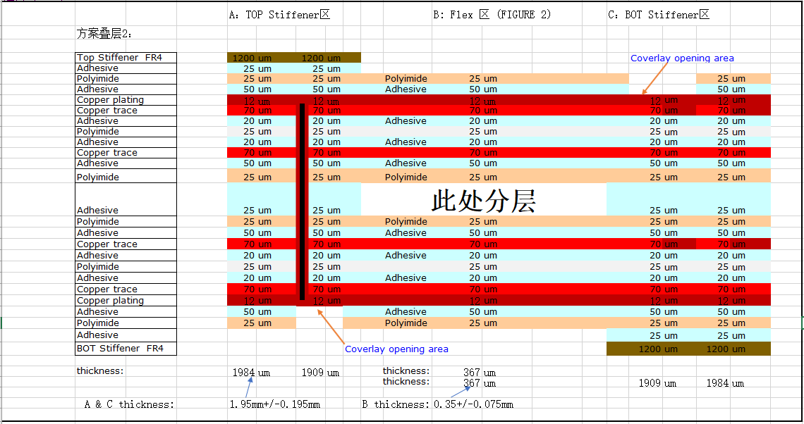
The flexible pcb board material system controls electrical insulation, bend behavior, temperature exposure, dimensional stability and manufacturing yield. A useful material review looks beyond the base film and includes the conductor, bonding system, coverlay, stiffeners, shielding and exposed-pad finish.

Exploded flexible PCB material stack with polyimide, copper, coverlay and connector stiffener
Material element What it does Selection question
Polyimide film Provides the flexible dielectric foundation and electrical insulation. What temperature, dimensional stability and bend-life conditions must the circuit withstand?
Rolled-annealed or electrodeposited copper Forms the conductors; copper grain structure and thickness influence flex fatigue and etching behavior. Is the application static, installation-flex or dynamic-flex, and what current and fine-line needs apply?
Adhesive or adhesiveless construction Bonds copper and dielectric layers or removes a separate adhesive layer from the core construction. Is lower thickness, tighter bending or repeated movement more important than the economics of a conventional construction?
Coverlay Protects conductors while leaving pads and contact areas exposed. Can the coverlay opening and adhesive flow be controlled around fine-pitch pads and bend transitions?
Stiffener Reinforces a connector, component or contact area without making the entire circuit rigid. Where must insertion force, component support or finished thickness be controlled?
Shielding layer Supports EMI control and reference continuity but adds thickness and can reduce flexibility. Does the electrical need justify the mechanical and cost trade-off?

Material names alone do not define performance. The copper weight, adhesive thickness, coverlay construction, plated features and local reinforcement all change the finished stack. For a deeper material review, see the BestPCBs guide to flexible PCB materials.

Which Flexible PCB Types Fit Different Layer and Bend Needs?

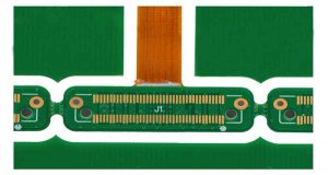
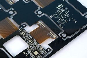
The main flexible pcb types are single-sided, double-sided and multilayer flex circuits, plus rigid-flex constructions that combine rigid and flexible sections. Choose the simplest structure that meets routing, shielding, current, connector and mechanical needs because every added layer increases thickness and makes the bend region harder to manage.

Type Best fit Main design watchpoint
Single-sided flex Simple jumpers, sensors, membrane interfaces and low-density interconnects. Limited routing and no plated connection between conductor sides.
Double-sided flex More routing density, plated-through connections and circuits needing conductors on both sides. Added copper and plating make the stack less compliant than a single-sided circuit.
Multilayer flex Dense signal routing, shielding, controlled references or complex interconnection. Layer count, bonded areas and via placement must be coordinated with the intended bend zones.
Rigid-flex PCB Assemblies that need component-bearing rigid areas connected by integrated flexible sections. The rigid-to-flex transition, layer construction and fabrication sequence require early supplier review.

Do not select a layer count from routing density alone. First identify the active bend area, then check whether reference planes, shielding, plated holes or bonded multilayer sections can stay outside it. A thinner, simpler flex tail connected to a rigid component area may be more reliable than forcing every electrical feature through a moving zone.

Flexible PCB Design Rules for Reliable Bending

Reliable flexible pcb design keeps mechanical strain low and avoids local stress concentrations. The bend region should be treated as a controlled mechanical feature, not as leftover routing space after the electrical layout is complete.

Static folded flex circuit and dynamic flex circuit moving through a smooth hinge bend
  • Define the motion: record whether the bend occurs once during assembly, occasionally during service or continuously through many cycles.
  • Route traces through the bend: use smooth, consistent paths and avoid abrupt width changes, sharp corners and unnecessary jogs in high-strain areas.
  • Keep discontinuities away: move vias, plated holes, component pads and stiffener edges out of the active bend wherever the design permits.
  • Stagger features: avoid creating a straight line of vias or pad edges that concentrates strain across the circuit width.
  • Manage copper direction: align conductor paths with the intended bending action and review plane or hatch patterns for both electrical and mechanical behavior.
  • Use gradual transitions: add suitable fillets, teardrops or other strain-relief geometry where conductors enter pads, subject to fabricator DFM rules.
  • Control the installed shape: prevent folds, pinching, torsion and contact with sharp housing edges.

Static and dynamic flex should not share an unexamined rule set. A circuit bent once and retained in a housing can often use a different stack and routing approach from a circuit moving in a hinge. Review bend direction, bend angle, available envelope, motion cycles and environmental conditions with the manufacturer before freezing the mechanical design.

How Do Flexible PCB Thickness, Bend Radius and Stiffeners Work Together?

Flexible pcb thickness and bend radius are linked: a thicker, more heavily bonded stack generally develops more strain for the same bend geometry. Stiffeners solve local support problems, but their edges also create transitions that must be kept away from active bending.

There is no single bend-radius multiplier that is safe for every flex circuit. The required radius depends on:

  • single-sided, double-sided or multilayer construction;
  • finished thickness and local thickness changes;
  • copper type, copper thickness and plating;
  • adhesive-based or adhesiveless materials;
  • static installation versus repeated dynamic movement;
  • trace orientation and density inside the bend;
  • coverlay, shielding and reinforcement; and
  • temperature, assembly constraints and expected service life.

Use IPC-2223 as a design reference, then obtain a stack-specific DFM review instead of treating one online ratio as a universal guarantee. The BestPCBs overview of IPC-2223 and flex PCB bend radius explains why construction and use conditions must accompany any bend recommendation.

What Are the Advantages and Disadvantages of a Flexible PCB?

A flex circuit can reduce interconnect volume, weight and assembly complexity, but it demands closer coordination between electrical, mechanical and manufacturing decisions. Its value should be judged at the assembly level, not by bare-board price alone.

Potential advantage Corresponding limitation
Routes through compact three-dimensional spaces. The installed bend and housing clearances must be controlled.
Can replace wires and connector interfaces. Design changes may require a new artwork, tooling or mechanical review.
Supports low-profile, lightweight assemblies. Thin circuits need suitable handling, fixtures and support during assembly.
Provides repeatable conductor routing. Poor bend-zone layout can create concentrated copper fatigue.
Can move with hinges or mechanisms when designed for dynamic use. Dynamic life depends on the complete material stack, geometry and motion profile.
May simplify final assembly and reduce interconnection count. Bare flex fabrication can cost more than a comparable simple rigid board.

A design that saves two connectors, a cable and manual routing time may reduce total installed cost even when the flex circuit itself has a higher unit price. Conversely, a simple stationary product with generous space may gain little from flexible construction.

What Drives Flexible PCB Board Price and Supplier Selection?

Flexible pcb board price is driven by the stackup, panel utilization, feature density, reinforcement, surface finish, testing and production volume. A useful quote therefore needs more than Gerber files and a layer count.

Common cost and manufacturability drivers include:

  • board outline, nesting efficiency and array or panel requirements;
  • material family, adhesiveless construction, copper type and copper thickness;
  • layer count, finished thickness and selective bonding requirements;
  • minimum trace, spacing, annular ring and hole features;
  • coverlay openings, fine-pitch pads and adhesive-flow control;
  • stiffeners, shielding films, pressure-sensitive adhesive and local reinforcement;
  • surface finish, impedance requirements and electrical testing;
  • prototype versus production quantity and repeat-order expectations; and
  • assembly fixtures, component loading and final functional tests when PCBA is included.
Engineer inspecting flexible PCB bend zones, traces and reinforced connector area

When comparing flexible pcb board manufacturers, ask each supplier to review the same controlled data package. Include fabrication files, drawing, stackup, material requirements, finished thickness, stiffener details, bend location, bend direction, minimum installed radius, expected motion cycles, surface finish, test requirements, quantities and assembly scope. This makes quotations more comparable and exposes DFM assumptions before they become production changes.

For a manufacturing-focused evaluation path, review BestPCBs’ flex PCB manufacturer page, then request written confirmation for the exact stackup and mechanical use case rather than relying on a generic capability statement.

Flexible PCB Board RFQ Checklist

A complete RFQ should define the mechanical life of the circuit as clearly as its electrical construction. The following inputs reduce avoidable assumptions during DFM and quotation.

  1. Gerber or ODB++ fabrication data, drill files, netlist and a controlled drawing.
  2. Layer stack, copper requirements, base film, coverlay and any adhesive restrictions.
  3. Finished thickness, thickness tolerance and local stiffener thickness.
  4. Bend-zone drawing with bend direction, angle, available radius and installed envelope.
  5. Static, installation-flex or dynamic-flex classification, including expected cycles for moving designs.
  6. Connector, contact-finger, component and assembly requirements.
  7. Surface finish, impedance, shielding, pressure-sensitive adhesive and marking requirements.
  8. Electrical test, dimensional inspection, reliability or functional-test requirements.
  9. Prototype quantity, production volumes, panel preferences and delivery destination.

Mark critical dimensions and bend restrictions on the drawing rather than leaving them in an email thread. If the supplier proposes a material or stack change, request an updated stackup and confirm its effect on thickness, impedance, bending and assembly interfaces before approval.

Frequently Asked Questions

Is a flex board the same as an FPC?

In most PCB manufacturing contexts, flex board, flexible circuit and FPC refer to the same product family: patterned conductors supported by a flexible dielectric. Individual suppliers may use the terms differently for product categories, so the fabrication drawing and stackup should define the construction instead of relying on the label alone.

Can a flexible PCB be bent repeatedly?

Yes, but only when it is designed for dynamic flexing. Repeated motion requires a compatible material stack, suitable copper, controlled thickness, smooth trace routing, an adequate bend radius and a defined motion path. A circuit designed only for installation flex should not be assumed to survive continuous hinge movement.

How many layers can a flexible PCB have?

Flexible circuits can be single-sided, double-sided or multilayer. The practical layer count depends on the fabricator, material set, routing density and whether the area must bend. More layers increase thickness and strain, so designers often keep active bend zones simpler than component or termination areas.

Why can a flexible PCB cost more than a rigid PCB?

Flex fabrication uses specialized films, coverlay processing, handling, reinforcement and inspection. Complex outlines and low panel utilization can also affect price. The relevant comparison is total assembly cost: a flex circuit may remove cables, connectors and manual wiring even when its bare-board price is higher.

Can components be mounted directly on a flexible PCB?

Yes. Component areas normally need suitable support, land patterns, assembly fixtures and strain control. Stiffeners are often used beneath connectors or component regions, while active bending is kept away from solder joints and abrupt stiffener edges.

Which surface finishes can be used on flexible PCB pads?

Several common PCB finishes can be applied, but the correct choice depends on pad function, soldering, contact wear, storage, assembly process and supplier capability. Connector fingers and solderable component pads may have different requirements, so define each finish area on the fabrication drawing.

Can controlled impedance be designed on a flex circuit?

Yes. Impedance control requires defined dielectric thickness, copper geometry, reference structure and material properties. Bending and stack transitions can affect geometry, so controlled-impedance regions and moving zones should be reviewed together with the fabricator.

Should vias be placed in a bend area?

Vias are stress discontinuities and should generally be kept outside an active bend when the layout allows. If packaging makes that impossible, the via construction, reinforcement, bend direction and use condition need an explicit DFM and reliability review.

Can a damaged flexible PCB be repaired?

Some pad, trace or component-area defects may be repairable under a controlled procedure, but damage in a repeatedly flexing region is difficult to restore reliably. Repair feasibility depends on access, conductor geometry, insulation restoration and the product’s reliability requirements.

What files are needed for a flexible PCB quote?

Provide fabrication data, drill files, a controlled drawing, stackup, material and thickness requirements, stiffener details, bend-zone geometry, motion classification, finish, testing needs and quantities. For assembly, also include the BOM, centroid data, assembly drawings and any programming or functional-test instructions.

Plan the Stackup Around the Bend Requirement

A dependable flex circuit starts with a defined mechanical use case. Establish the bend zone and motion profile first, then select materials, copper, layer count, thickness, stiffeners and routing that support that requirement. Complete drawings and early DFM review are more valuable than applying a generic bend rule after layout.

If you need a flex PCB fabrication or assembly review, send the BestPCBs engineering team your files, stackup, quantities, bend radius and motion-cycle requirements at sales@bestpcbs.com. The team can review manufacturability and prepare a project-specific quotation.
You may also like

Solders and Flux in PCB Assembly | Materials & Quality Guide

July 20th, 2026

Solders and flux are basic materials in electronics soldering, but they directly affect PCB assembly quality, solder joint reliability, cleanliness, inspection results, and long-term product performance. Solder creates the metal connection. Flux prepares the metal surfaces so solder can wet the pads and component leads properly.

For PCB and PCBA projects, solders and flux are not just workshop supplies. They are part of the manufacturing process. The wrong solder alloy, flux type, solder paste condition, cleaning method, or residue control plan can lead to poor wetting, solder balls, bridges, corrosion risk, electrical leakage, weak joints, or failed inspection. EBest Circuit (Best Technology) supports PCB fabrication, component sourcing, SMT assembly, through-hole assembly, inspection, testing, cleaning, and packing for custom PCBA projects. If you are preparing a PCB assembly project, send your Gerber files, BOM, assembly drawing, soldering notes, or quality requirements to sales@bestpcbs.com for engineering review before production.

solders and flux

What Are Solders and Flux in PCB Assembly?

In PCB assembly, solder is the metal alloy used to join electronic components to PCB pads. Flux is the chemical material that removes surface oxides, improves wetting, and helps solder flow onto the metal surfaces.

They work together, but they are not the same.

MaterialMain Role
SolderForms the metal joint
FluxPrepares surfaces for soldering
Solder pasteSolder powder mixed with flux
Flux residueMaterial left after soldering

In manual soldering, solder may come as solder wire, often with a flux core. In SMT assembly, solder is commonly applied as solder paste through a stencil. The paste already contains solder powder and flux, so storage, printing, reflow profile, and inspection all matter.

For PCB manufacturers and PCBA suppliers, the goal is not simply to “use solder and flux.” The goal is to choose and control them correctly for the board, components, assembly process, cleanliness requirement, and reliability target.

solders and flux

How Solders and Flux Work Together in Soldering

Solder does not bond well to oxidized metal. PCB pads, component leads, copper, tin, nickel, and other solderable surfaces can develop oxide layers before or during heating. Flux helps remove or reduce these oxides so molten solder can spread and form a stronger joint.

A good soldering result depends on three things working together:

  • Clean solderable surfaces
  • Correct heat transfer
  • Suitable solder and flux chemistry

When flux activates under heat, it helps solder wet the pad and component termination. Good wetting usually creates a smooth, shiny, well-formed joint, depending on the solder alloy and process. Poor wetting may create dull, rough, incomplete, or weak solder joints.

In PCBA production, this is why soldering is controlled as a process, not treated as a manual habit. Solder paste condition, stencil printing, reflow curve, component finish, pad finish, flux activity, and cleaning requirements all affect final quality.

Soldering Wire and Flux for PCB Hand Soldering

Soldering wire and flux are commonly used for hand soldering, repair, connector assembly, through-hole components, rework, and small production steps that cannot be completed only by SMT.

Solder wire may be:

  • Lead-free solder wire
  • Tin-lead solder wire where allowed
  • Flux-core solder wire
  • No-clean solder wire
  • Rosin-core solder wire

For PCB assembly, hand soldering is often used for:

  • Connectors
  • Wires and cables
  • Switches
  • Large through-hole components
  • Post-SMT repair
  • Prototype modification

The key is process control. Too little flux can cause poor wetting. Too much flux can leave excessive residue. Too much heat can damage pads, components, or laminate. Too little heat can create cold solder joints.

At EBest Circuit, hand soldering is treated as part of the SMT PCB assembly process. It should follow assembly notes, component sensitivity, soldering temperature requirements, cleanliness requirements, and inspection standards.

Soldering Paste vs Flux in SMT Assembly

Soldering paste vs flux is a common question because both are used in electronics soldering, but they have different roles.

Solder paste is a mixture of solder powder and flux. Flux alone does not create a metal joint. It only supports the soldering process.

ItemWhat It ContainsMain Use
FluxChemical activatorsHelps solder wet surfaces
Solder wireSolder alloy, often flux coreHand soldering
Solder pasteSolder powder + fluxSMT reflow assembly

In SMT assembly, solder paste is printed onto PCB pads through a stencil. Components are placed onto the paste, then the board passes through reflow soldering. During reflow, the flux activates, the solder powder melts, and solder joints form.

This is why solder paste handling is important. Paste storage, thawing time, stencil thickness, printing pressure, SPI inspection, placement accuracy, and reflow profile all affect PCBA quality.

So, is soldering paste and flux the same? No. Solder paste contains flux, but flux is only one part of solder paste.

solders and flux

Types of Soldering Flux for Electronics Manufacturing

There are several types of soldering flux used in electronics. The right choice depends on the assembly process, components, board finish, cleaning requirement, and reliability level.

Flux TypeTypical Use
Rosin fluxGeneral electronics soldering
No-clean fluxLow-residue PCBA processes
Water-soluble fluxStronger activity, requires cleaning
Organic acid fluxSelected electronics applications
Inorganic acid fluxNot suitable for normal PCB assembly

For PCB assembly, aggressive acid fluxes used for plumbing or metalwork should not be used on electronic circuit boards. They may cause corrosion or reliability problems.

No-clean flux is common in electronics manufacturing, but “no-clean” does not always mean residue can be ignored. If the board has fine-pitch ICs, high impedance circuits, RF areas, conformal coating, connector areas, or customer cleanliness requirements, residue should still be reviewed.

For reliable PCBA, flux selection should match the product’s use environment and inspection requirements, not only the soldering convenience.

solders and flux

Flux Core Solder, Liquid Flux, and Paste Flux Selection

Flux core solder, liquid flux, and paste flux are different delivery forms. They are chosen based on how the soldering process is performed.

FormBest Fit
Flux core solderManual soldering
Liquid fluxSelective use or rework
Paste fluxRework and localized soldering
Solder pasteSMT production

Flux core solder is convenient for hand soldering because the flux is inside the wire. Liquid flux can be applied to improve solderability in specific areas. Paste flux is often used in rework or localized repair. SMT solder paste is used for stencil printing and reflow assembly.

For production, selection should consider:

  • Component type
  • Pad finish
  • Solder alloy
  • Cleaning method
  • Residue tolerance
  • Inspection requirement
  • Reflow or hand soldering process
  • Customer quality standard

In a PCBA factory, these materials should be controlled by process notes, not selected casually by operator preference.

solders and flux

PCB Flux and Circuit Board Flux Residue Risks

PCB flux and circuit board flux are useful during soldering, but flux residue can become a quality risk if it is not controlled.

Possible residue-related issues include:

  • Sticky or visible contamination
  • Poor appearance after assembly
  • Connector contact concerns
  • Difficulty with conformal coating
  • Ionic contamination risk
  • Electrical leakage in sensitive circuits
  • Corrosion under certain conditions
  • Customer inspection rejection

Not every residue causes failure, and many no-clean residues are acceptable under the right process. However, the decision depends on board application, cleanliness requirement, circuit sensitivity, and operating environment.

For example, a simple consumer board may tolerate more residue than a medical device, automotive module, sensor board, RF module, high-impedance circuit, or product used in humid environments.

This is where manufacturing review matters. The supplier should understand whether the board requires visual cleanliness, ionic cleanliness, conformal coating compatibility, or special post-assembly cleaning.

How to Clean Flux from PCB After Assembly

How to clean flux from PCB depends on the flux type, board design, components, and customer requirement. Some boards are cleaned after soldering, while some no-clean assemblies may not require full washing.

Common cleaning considerations include:

CheckpointWhy It Matters
Flux typeDetermines cleaning method
Component sensitivitySome parts cannot be washed
Connector areasResidue can affect contact
Dense SMT zonesResidue can hide under parts
Coating requirementSurface must be compatible
Customer standardDefines acceptance level

Cleaning may involve approved solvents, aqueous cleaning, manual cleaning, or controlled process cleaning. The cleaning method should not damage labels, components, connectors, switches, displays, sensors, or unsealed parts.

For PCBA projects, cleaning should be confirmed before production, especially when the customer says the board must have no solder balls, no residue, no visible contamination, or needs conformal coating after SMT.

A clean board is not only about appearance. It can affect inspection, reliability, packing, and customer confidence in the finished assembly.

How EBest Circuit Controls Solders and Flux in PCBA Quality

At EBest Circuit, solders and flux are controlled as part of the full PCB assembly process. The goal is to make the board manufacturable, solderable, inspectable, and reliable for the customer’s real application.

Our PCBA support may include:

  • PCB fabrication and surface finish review
  • BOM and component package review
  • SMT assembly process planning
  • Solder paste printing and SPI
  • Reflow soldering control
  • AOI inspection
  • X-Ray inspection for BGA when required
  • Through-hole and connector soldering
  • Cleaning and visual inspection
  • Functional testing coordination
  • Packing based on customer requirements

For prototype and small-batch projects, EBest Circuit can also help engineers review assembly risks before production. This is especially useful when the board includes fine-pitch components, connectors, BGA, impedance-controlled circuits, high-power areas, or cleanliness requirements.

Solders and flux may look like small production materials, but in PCBA manufacturing they affect the final result. A good supplier should understand how material choice, soldering process, inspection, cleaning, and documentation work together.

FAQs about Solders and Flux in PCB Assembly

1. Are solders and flux the same?
No. Solder is the metal alloy that forms the joint. Flux is the chemical material that helps remove oxides and improve solder wetting.

2. Is soldering paste and flux the same thing?
No. Soldering paste contains solder powder and flux. Flux is one part of solder paste, but flux alone cannot create a solder joint.

3. What types of soldering flux are used in electronics?
Common electronics flux types include rosin flux, no-clean flux, water-soluble flux, and selected organic acid fluxes. Aggressive acid flux for plumbing is not suitable for normal PCB assembly.

4. Does no-clean flux need to be cleaned from PCB assemblies?
Not always. No-clean flux is designed to leave acceptable residue under the right process. However, cleaning may still be needed for fine-pitch boards, coating, high-reliability products, or customer cleanliness requirements.

5. How does flux residue affect PCB assembly quality?
Flux residue may affect appearance, connector contact, coating adhesion, electrical leakage, corrosion risk, or customer inspection. The real risk depends on flux type, residue amount, circuit sensitivity, and operating environment.

6. Can EBest Circuit help review solders and flux requirements for PCBA projects?
Yes. EBest Circuit can review PCB files, BOM, assembly notes, soldering requirements, cleaning requirements, and testing needs before production. For custom PCB and PCBA projects, you can send your files or questions to sales@bestpcbs.com.
If your PCB assembly project involves soldering, flux residue, PCB cleaning, SMT, through-hole assembly, BGA, connectors, or quality inspection requirements, please feel free to contact us at sales@bestpcbs.com. If you are still comparing soldering flux vs soldering paste for your assembly process, EBest Circuit’s engineering team can help review your manufacturing files and process notes before production, so your PCBA project can move from files to finished boards with fewer avoidable risks.
You may also like

Standard PCB Via Sizes Guide with Size Chart and Design Rules

July 20th, 2026

Are standard PCB via sizes limiting routing space or leaving too little fabrication margin? Define the finished hole, pad diameter, annular ring, board thickness, and connection depth together. Start with the largest geometry that fits the routing field and passes the selected fabrication process.

The chart below compares standard PCB via sizes in millimeters and mils, then shows how plating, drilling tolerance, current, signal speed, and via type change the final choice. Use it to build early layout rules, but release fabrication data only after checking the stackup and drill table together.

Standard PCB via sizes shown on a circuit board at an optical inspection bench

What Are Standard PCB Via Sizes?

A via library must pair the finished hole with its copper pad. Common starting geometries include a 0.30/0.60 mm finished-hole/pad pair for ordinary multilayer routing and 0.20/0.45 mm for tighter layouts. Release either combination only after checking board thickness, copper weight, product class, and the confirmed drill table.

A library rule should store at least the finished hole, pad diameter, plane anti-pad, solder-mask opening, and permitted connection depth. Naming a via only as “0.30 mm” is incomplete because that value could describe the hole, drill tool, or pad.

Standard PCB Via Sizes Chart in mm and Mils

These values are illustrative, not universal IPC limits. These standard PCB via sizes show practical mechanically drilled plated-through-via combinations. Values are rounded because one mil equals 0.0254 mm. The hole column is a finished-hole target; the production drill is normally larger to allow for deposited copper.

Finished Hole (mm) Finished Hole (mil) Pad Diameter (mm) Pad Diameter (mil) Ideal Ring Based on Finished Hole
0.20 mm 7.9 mil 0.45 mm 17.7 mil 0.125 mm / 4.9 mil
0.25 mm 9.8 mil 0.55 mm 21.7 mil 0.150 mm / 5.9 mil
0.30 mm 11.8 mil 0.60 mm 23.6 mil 0.150 mm / 5.9 mil
0.40 mm 15.7 mil 0.80 mm 31.5 mil 0.200 mm / 7.9 mil
0.50 mm 19.7 mil 1.00 mm 39.4 mil 0.250 mm / 9.8 mil

These combinations are not acceptance limits. Compare them with the latest capability data, including minimum finished hole, annular ring, drill-to-copper clearance, board thickness, and any special registration allowance.

How Are Standard PCB Via Sizes Measured?

Define the hole and pad separately. The drawing must identify whether a stated via size means the hole or the complete copper pad. The finished hole is the open diameter after plating, while the production drill is normally larger because deposited copper reduces the opening. The pad diameter is the outside copper diameter, while the annular ring is the radial copper width between the finished hole and pad edge.

  • Finished hole: The plated opening used in the finished board.
  • Tool diameter: The drill chosen before hole-wall copper is deposited.
  • Pad diameter: The total copper land surrounding the hole.
  • Annular ring: The radial copper width around the hole after registration effects.

For standard PCB via sizes, distinguish an ideal centered ring from the minimum remaining ring after drill offset. The ideal value supports library calculations; the minimum value determines whether the finished feature meets the selected acceptance criteria.

Label every PCB via drill size chart with units, plated status, finished-hole tolerance, and whether each dimension is a nominal tool or finished opening. Apply the same definitions in CAD, NC drill, fabrication drawings, and CAM review.

How Do Standard PCB Via Sizes Compare by Via Type?

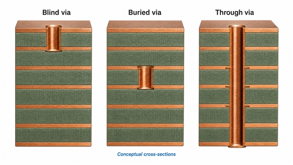
Connection depth and drilling method define the via family. A through via crosses the entire board, a blind via connects an outer layer to selected inner layers, and a buried via remains between inner layers. A microvia is a shallow HDI interconnect generally formed by laser processing, historically defined in IPC material as no more than 150 μm in diameter.

Via Type Typical Connection Common Size Direction Main Control
Through via Top to bottom Largest mechanical range Full board aspect ratio
Blind via Outer to inner Often smaller; stackup-dependent Controlled depth and registration
Buried via Inner to inner Stackup-dependent Sequential lamination plan
Microvia Usually adjacent layers Up to 0.15 mm under the historical definition Laser geometry and target-pad interface

Size alone does not identify the construction. A 0.15 mm feature may be a laser microvia in a thin dielectric or an advanced mechanical hole in a different stackup, and those processes have different aspect-ratio and target-pad controls.

Choose the via family before assigning standard PCB via sizes. Through vias usually offer the simplest fabrication path, while blind, buried, and stacked microvia structures add layer-pair documentation, lamination planning, and interface-reliability checks.

For a deeper classification, review PCB Via Types before choosing a drill method.

What Factors Control Standard PCB Via Sizes?

Choose the largest via that preserves required clearances. Start with stackup depth and available escape space. Then compare standard PCB via sizes against plating, annular ring, drill-to-copper clearance, current path, and signal transition. Also check solder-mask treatment and whether the via will be filled or placed in a component pad.

  • Stackup depth: Deeper holes raise the drilling and plating challenge.
  • Routing field: Fine-pitch packages may force smaller pads or blind structures.
  • Electrical role: Signal, return, power, and thermal paths impose different priorities.
  • Fabrication margin: Registration and drill tolerance can reduce the remaining ring.
  • Assembly interface: Via-in-pad, exposed holes, and solder wicking may require filling or capping.

Apply these checks to standard PCB via sizes in sequence: confirm the stackup and connection depth, reserve routing space, assign the electrical or thermal role, and then verify fabrication margin. This order prevents a convenient CAD default from becoming an unsupported manufacturing requirement.

How to Calculate Standard PCB Via Sizes and Annular Ring Width?

Calculate the ideal ring first, then add process margin. The basic geometry is simple, but the released pad must also cover drill compensation, positional error, and layer registration.

  1. Define the hole reference. Confirm whether the drawing specifies a plated finished hole or a production drill-tool diameter. Do not mix the two in one calculation.
  2. Calculate the centered nominal ring. Use AR = (Pad Diameter − Hole Diameter) ÷ 2. A 0.60 mm pad around a 0.30 mm finished hole gives a 0.15 mm ideal ring.
  3. Estimate the production drill. The tool is normally larger than the finished opening because barrel copper reduces the hole. The exact compensation belongs to the confirmed fabrication process.
  4. Check the fabrication ring. Recalculate against the production drill where the CAM rule uses tool size. If a 0.30 mm tool is used with a 0.45 mm pad, the geometric ring before positional allowances is only 0.075 mm.
  5. Apply tolerance and registration allowances. Subtract drill wander and layer-to-layer misregistration from the ideal condition. Check internal and external lands separately because their acceptance rules may differ.
  6. Round up to a supported pad. Select the next manufacturable library value when the calculated minimum falls between available rules. Recheck drill-to-copper clearance and routing escape after increasing the pad.

For reverse calculation, use Pad Diameter = Hole Diameter + 2 × Required Ring, then add any supplier-defined fabrication allowance. A PCB via pad size calculator verifies geometry; the drill table and capability review determine whether the result can be released.

How Does Board Thickness Affect Via Size and Aspect Ratio?

Board thickness directly affects via aspect ratio. A thicker connection depth generally requires a larger hole because copper must plate uniformly along a longer barrel. Via aspect ratio is commonly expressed as connection depth divided by hole or drill diameter, using the fabricator’s stated convention. For a 1.60 mm through connection and a 0.30 mm hole, the simple ratio is about 5.3:1.

The same 0.30 mm hole becomes more demanding on a 2.40 mm board at about 8:1. Blind vias use the actual layer-to-layer depth rather than full board thickness. Confirm whether the capability limit uses drilled or finished diameter before comparing values.

Aspect ratio influences desmear access, activation, and copper distribution along the barrel. For standard PCB via sizes near a process limit, increasing the hole, reducing connection depth, or changing the via structure usually provides more robust margin than relying on a nominal maximum.

Match every PCB via aspect ratio chart to the supplier’s drilled- or finished-diameter convention. Record that convention beside the limit so reviewers calculate the same ratio.

Modern metallographic inspection of an unfilled plated through-hole via cross-section

What Is the Minimum Practical Via Size for PCB Manufacturing?

A 0.25 or 0.30 mm hole often provides better process margin. A 0.20 mm finished mechanical hole may be available, but its suitability depends on stackup depth, drilling, plating, and registration capability. Smaller geometry also affects tool life, panel loading, and inspection controls.

Do not select a minimum hole from a generic chart alone. Check the finished-hole range, tool increment, annular ring, aspect ratio, copper thickness, and the distinction between prototype and volume capability. The related PCB drill sizes guide explains why tool and finished dimensions differ.

For volume production, standard PCB via sizes must remain repeatable across the intended quantity, material system, panel format, and inspection plan. A prototype capability may be technically possible but unsuitable as the default production rule.

If routing allows, moving from a 0.20 mm hole to 0.25 or 0.30 mm can improve drill life, plating access, and registration margin. Use the smaller option where it solves a specific density problem rather than as an automatic board-wide choice.

How to Choose Via Sizes for Signal, Power and Thermal Vias?

Via function determines the sizing priority. Signal transitions emphasize geometry and return paths, while power and thermal structures emphasize parallel copper area, temperature rise, and heat spreading.

  • Ordinary signal vias: Start with a repeatable mechanical size that preserves annular ring and routing clearance. Keep the library uniform unless escape routing or electrical performance justifies another family.
  • Power vias: Evaluate the finished barrel diameter, plated copper thickness, allowable temperature rise, connected plane area, and the number of vias in parallel. Do not assign current capacity from drill diameter alone.
  • Thermal vias: Use an array to connect the heat source to useful copper on other layers. Balance hole size, pitch, copper spreading area, board thickness, solder-mask treatment, and assembly behavior.
  • Return-path vias: Place ground transitions close to signal layer changes so return current does not take a wide detour. The spacing should follow the interface frequency and field-solver or layout review.
  • Via-in-pad structures: Confirm filling, planarization, and copper capping when the via sits inside a solderable land. An open via can wick solder and reduce joint consistency.

Use several vias when parallel paths improve current distribution or thermal transfer, but preserve enough copper between holes. Final quantity should come from electrical and thermal analysis plus the fabricator’s minimum hole spacing.

How to Select Via Sizes for High-Speed PCBs?

Treat a high-speed via as a complete transition. Hole and pad size affect the result, but barrel length, unused stub, anti-pad, reference planes, and nearby return vias usually matter just as much.

  • Start with the real stackup: Use actual dielectric thicknesses, copper layers, finished board thickness, and the layers connected by the via. A generic 2D rule cannot represent the transition correctly.
  • Control pad capacitance: A smaller pad can reduce local capacitance, but it also reduces registration margin. Adjust the pad and plane anti-pad together rather than shrinking one feature in isolation.
  • Limit unused barrel: A long open stub can create resonant behavior. Consider blind vias or backdrilling when simulation shows that the stub affects the required data rate or insertion-loss budget.
  • Preserve the return path: Add nearby ground vias when a signal changes reference planes. Keep them close enough to limit the return-loop area without violating spacing or anti-pad rules.
  • Review differential symmetry: Match via count, pad geometry, anti-pads, reference transitions, and breakout routing for both members of a differential pair.
  • Validate the launch: Model the package or connector breakout with the via transition. Confirm impedance, reflection, crosstalk, and loss before freezing the drill library.

Do 2-Layer, 4-Layer and Multilayer PCBs Require Different Via Sizes?

Layer count alone does not set via diameter. Board thickness, plane arrangement, routing density, and connection depth often change the result. A 2-layer and 4-layer board can share the same 0.30/0.60 mm rule when thickness and clearances match. A dense multilayer board may require smaller pads, blind vias, or backdrilling even when the finished through-hole remains unchanged.

  • Two-layer boards: Thickness and copper clearance usually control the rule because there are no internal plane anti-pads or buried connections.
  • Four-layer boards: The same hole may remain practical, but internal plane clearances and return-path transitions require review.
  • Higher-layer-count boards: Increased thickness, dense escape routing, multiple reference planes, and sequential structures can justify smaller pads, backdrilling, or blind vias.

Do not shrink the through-hole merely because the board has more layers. First determine whether the real constraint is aspect ratio, anti-pad congestion, BGA escape, unused stub length, or a local connection that does not require the full board depth.

What Do IPC Standards Say About PCB Via Sizes?

IPC does not mandate one universal via diameter. Its documents define design principles, product classes, qualification, performance, and acceptance criteria. Standard PCB via sizes must still match the selected construction. IPC-2221 supports generic board design, the IPC-6012 family addresses rigid-board performance, and HDI structures require applicable sectional guidance and purchasing specifications.

State the required product class and acceptance criteria on the fabrication documentation. Also verify the revision, amendments, and contractual hierarchy in force for the order. A preferred library value does not replace the finished-board acceptance requirements.

Use IPC documents for design principles and acceptance language, then apply approved supplier limits for drills, pads, and aspect ratios. Do not specify an “IPC standard PCB via size” without the stackup, product class, and manufacturing process.

For HDI structures, document the layer pair, dielectric depth, target pad, stacking or staggering method, fill requirement, and qualification evidence. These details carry more engineering value than quoting a microvia diameter by itself.

How Do Drilling and Plating Tolerances Affect Finished Via Size?

Plating makes the finished opening smaller than the drilled hole. The drill tool creates the initial opening before copper is deposited on the barrel. Tool wear, spindle position, material movement, layer registration, desmear, and copper distribution influence the final geometry. Consequently, the fabrication drawing should distinguish plated finished holes from drill-tool data and identify tolerances clearly.

Pad size must preserve acceptable copper after these variations. A nominal 0.15 mm geometric ring can become smaller at the finished board when the hole shifts toward one pad edge, so production allowance cannot be removed from the calculation.

Build the tolerance chain for standard PCB via sizes from the production drill, expected plating reduction, finished-hole tolerance, drill position, and layer registration. The worst-case condition is not the centered nominal ring shown in a CAD library.

Specify the required finished opening where component fit or pin insertion matters. For ordinary vias, confirm the supplier’s standard finished-hole tolerance and avoid imposing a tighter tolerance unless the function supports it.

What Via Size Problems Can Reduce PCB Reliability?

Small holes in thick boards increase plating and thermal risk. Geometry outside proven drilling, cleaning, plating, registration, or thermal-cycling limits can cause ring loss, partial breakout, uneven barrel copper, resin smear, voids, barrel cracks, pad lifting, and weak microvia target interfaces.

  • Ring loss: Drill offset leaves too little copper around the finished hole.
  • Barrel weakness: Poor hole preparation or plating distribution raises crack and open-circuit risk.
  • Thermal stress: Z-axis expansion loads the copper barrel during assembly and service cycles.
  • Microvia interface failure: Stacked structures require controlled construction and suitable performance evidence.

Match each risk to evidence. Cross-sections can reveal barrel copper, voids, smear removal, and internal connections; electrical testing verifies net continuity; thermal-stress coupons can expose latent interconnect weakness under the specified acceptance plan.

Do not treat a visually centered surface pad as proof that every internal layer has adequate copper. Internal registration and pad breakout require the applicable inspection method and acceptance criteria.

Optical inspection workstation used to verify PCB via holes and annular rings

PCB Via Size Selection Example for a Multilayer Board

Begin with a manufacturable baseline. Consider a 1.60 mm, six-layer control board with ordinary signal routing, power planes, and one fine-pitch device. Start the general through-via library at a 0.30 mm finished hole with a 0.60 mm pad.

The centered nominal ring is 0.15 mm, and the simple finished-hole aspect ratio is about 5.3:1. These figures are screening values. CAM must still check the production drill, internal lands, registration allowance, copper weight, and plane anti-pads.

Use the baseline via for unrestricted signal transitions and suitable ground returns. Review power and thermal locations separately because their via count, connected copper, temperature rise, and assembly conditions differ from ordinary signal routing.

If the 0.60 mm pad blocks escape channels under the fine-pitch device, do not shrink every via on the board. Evaluate a local 0.20/0.45 mm mechanical rule only after capability confirmation, or use an HDI PCB fabrication structure where the stackup supports laser microvias.

Release the design only after the drill table identifies finished versus tool diameters and every via family passes annular-ring, aspect-ratio, clearance, electrical, thermal, and filling checks.

How Can We Optimize Via Sizes Before PCB Manufacturing?

Optimize vias before releasing fabrication data. Remove duplicate drill families, recover routing space where required, and keep every critical via inside the confirmed process window.

  1. Freeze the stackup: Record finished thickness, copper weights, dielectric depths, sequential laminations, and the actual connection depth of each blind or buried structure.
  2. Classify via functions: Separate ordinary signal, return, power, thermal, high-speed, blind, buried, microvia, backdrilled, and via-in-pad requirements.
  3. Normalize the drill library: Reuse practical hole-and-pad pairs where their electrical and physical roles match. Remove duplicate sizes that create tooling complexity without adding value.
  4. Run geometric checks: Calculate ideal ring, production-drill ring, aspect ratio, drill-to-copper clearance, hole spacing, anti-pad clearance, and board-edge distance.
  5. Review special treatments: Confirm tenting, plugging, resin filling, planarization, copper capping, and backdrilling before they become quotation or assembly surprises.
  6. Validate electrical and thermal roles: Check current sharing, temperature rise, heat spreading, return continuity, differential symmetry, stub length, and modeled transition performance where applicable.
  7. Complete fabrication DFM: Compare the drill table and stackup with confirmed tolerances, registration capability, plating process, inspection method, and acceptance class.

Send Gerber or ODB++, NC drill data, stackup, copper requirements, hole tolerances, impedance information, and special-via notes as one controlled package. Cross-check the drawing, drill file, netlist, and quotation notes so they describe the same geometry and treatment.

FAQs About Standard PCB Via Sizes

Q1: Why can a filled via develop a surface dimple?

A1: Resin shrinkage or incomplete planarization can leave a depression. Specify fill, cure, planarization, and copper-cap acceptance when surface flatness affects an assembly pad.

Q2: Should nonfunctional internal pads be removed?

A2: Removal can improve clearance, but it changes mechanical and electrical behavior. Decide by stackup, reliability class, signal performance, and the fabricator’s approved practice.

Q3: When are teardrops useful at via connections?

A3: Teardrops add copper where a narrow trace enters a pad. They can improve tolerance to registration or etching variation when permitted by the layout and acceptance rules.

Q4: How close can a via be placed to a routed board edge?

A4: The limit depends on finished edge tolerance and required copper clearance. Measure from the relevant copper or drilled feature and include routing movement, plating exposure, and any edge-metal requirement.

Q5: Can solder mask cover only one side of a via?

A5: Yes, asymmetric mask treatment is possible when clearly documented. Confirm whether the intent is tenting, partial plugging, test access, or solder-flow control.

Q6: Why do thermal-pad vias sometimes wick solder?

A6: An open barrel provides a path for molten solder. Hole size, stencil design, mask treatment, fill method, and reflow conditions determine whether wicking becomes significant.

Q7: Can a plated via be placed in a flex bend area?

A7: Avoid it unless the rigid-flex construction specifically supports it. A plated barrel concentrates strain and may crack during repeated bending, so keep vias in supported rigid regions where possible.

Q8: How should blind and buried vias appear in fabrication data?

A8: Separate drill files should identify each layer pair or controlled depth. The stackup drawing must agree with those files and show the required lamination sequence.

Q9: Are vias included in bare-board electrical testing?

A9: Vias are normally part of the tested net connectivity. Confirm the test method, coverage, and special coupon requirements when intermittent barrel or microvia reliability is a concern.

Q10: What causes copper-cap cracking over a filled via?

A10: Fill voids, material mismatch, or thermal stress can damage the cap. Control hole preparation, fill quality, cure, planarization, cap plating, and thermal acceptance criteria.

Conclusion

Match the full via geometry to the stackup and process. Verify standard PCB via sizes by checking the hole, pad, annular ring, connection depth, and fabrication tolerance for each signal, power, thermal, blind, buried, or microvia structure.

EBest provides custom PCB production support for prototypes and volume orders. Send Gerber/ODB++, NC drill files, stackup, copper requirements, quantity, and special via notes to sales@bestpcbs.com for a manufacturability review and quotation.

You may also like

Circuit Card vs Circuit Board | Circuit Card Assembly Guide

July 20th, 2026

A circuit card vs circuit board comparison can be confusing because engineers, buyers, assemblers, and different industries may use these terms in different ways. In many cases, a circuit board means the bare printed circuit board, while a circuit card may refer to a board used as a plug-in card, or an assembled board with components.

For manufacturing projects, the more important question is not only the name. It is whether the project needs bare PCB fabrication, circuit card assembly, component sourcing, SMT assembly, testing, conformal coating, or final packing. EBest Circuit (Best Technology) supports custom PCB manufacturing and PCBA assembly for engineers who need a practical manufacturing partner. If you are preparing Gerber files, BOM, assembly drawings, stackup notes, or test requirements, you can send them to sales@bestpcbs.com for engineering review before production.

Circuit card vs circuit board

Circuit Card vs Circuit Board: What Is the Real Difference?

A circuit board usually refers to the physical printed circuit board that carries copper traces, pads, vias, solder mask, and surface finish. Before components are assembled, it is often called a bare PCB.

A circuit card can mean different things depending on the industry. In some documents, it simply means a PCB card. In other cases, especially in purchasing, assembly, industrial electronics, aerospace electronics, and equipment documentation, circuit card often means an assembled electronic card.

The practical difference is this:

TermCommon Meaning
Circuit boardBare PCB or general board
Circuit cardPCB card or assembled card
Circuit card assemblyPCB assembled with components
PCBAPrinted circuit board assembly
PWBPrinted wiring board, often bare board

So when a customer asks for a circuit card, the manufacturer should not assume the scope immediately. The right question is whether the customer needs only PCB fabrication, or a completed circuit card assembly services.

Circuit card vs circuit board

What Is a Circuit Card Assembly?

A circuit card assembly, often shortened as CCA, is a printed circuit board after electronic components have been mounted and soldered onto it.

A bare PCB may include:

  • FR4, polyimide, ceramic, metal core, or other base material
  • Copper traces and planes
  • Plated through holes, blind vias, buried vias, or microvias
  • Solder mask and silkscreen
  • Surface finish such as HASL, ENIG, immersion silver, or OSP

A circuit card assembly may include all of the above, plus:

  • ICs, connectors, resistors, capacitors, sensors, and modules
  • SMT and through-hole soldering
  • AOI, X-Ray, electrical testing, or functional testing
  • Cleaning, conformal coating, programming, and packing when required

This is why CCA and PCBA are closely related terms. For many practical manufacturing projects, circuit card assembly and PCBA refer to the same production stage: the board is no longer just a bare PCB; it has become an assembled electronic unit.

Circuit Board Card, PCB Card, and Printed Circuit Card Terms

Many buyers search terms such as circuit board card, PCB card, or printed circuit card because they are trying to describe a board that works like a removable or functional electronic card.

These terms may appear in:

  • Industrial control systems
  • Test equipment
  • Communication equipment
  • Power control modules
  • Medical electronics
  • Automotive electronics
  • Aerospace electronics
  • Embedded computing systems

For example, a plug-in control board inside industrial equipment may be called a circuit card by the equipment manufacturer. A PCB supplier may call the same item a PCB assembly or PCBA. A procurement document may call it a card assembly.

The wording is different, but the manufacturing information still needs to be clear:

Required FileWhy It Matters
Gerber or ODB++Defines PCB fabrication
Stackup drawingDefines layers and thickness
BOMDefines components
Pick-and-place fileDefines placement
Assembly drawingDefines orientation and notes
Test requirementsDefines final inspection

If the files are complete, the manufacturer can identify whether the order is a bare PCB project, a circuit card assembly project, or a turnkey PCBA project.

Printed Wiring Board vs Circuit Card Assembly

Printed wiring board vs circuit card assembly is another common terminology issue.

A printed wiring board, or PWB, is usually another name for a bare PCB. It emphasizes the copper wiring pattern on the board. A circuit card assembly is a later stage, after components are installed.

The difference is simple:

ItemBare Board?Components?
PWBYesNo
PCBUsually yesNo
PCBANoYes
CCANoYes

This distinction matters in RFQs, drawings, and purchase orders. If a buyer sends only Gerber files and asks for circuit cards, the supplier may need to confirm whether the order includes components and assembly. If the buyer sends Gerber, BOM, placement files, and test notes, the project is more likely a circuit card assembly or PCBA order.

For EBest Circuit, this confirmation step is important because PCB fabrication and PCBA assembly require different engineering checks, production planning, lead time, and quality control.

CCA vs PCBA: When Does a PCB Become an Assembly?

A PCB becomes an assembly when components are mounted and soldered onto the board. That is the main difference in CCA vs PCBA discussions.

In many industries, CCA and PCBA are used almost interchangeably. The difference is often based on customer terminology rather than manufacturing reality.

CCA is common in:

  • Industrial electronics
  • Aerospace electronics
  • Equipment maintenance documents
  • Contract manufacturing documentation
  • System-level assembly projects

PCBA is common in:

  • PCB manufacturing
  • SMT assembly
  • Consumer electronics
  • IoT products
  • Medical devices
  • Automotive modules

From a manufacturing point of view, the key is not which term is used. The key is whether the supplier understands the full build requirement: bare board fabrication, component sourcing, SMT, through-hole assembly, inspection, testing, programming, coating, packing, and documentation.

Circuit card vs circuit board

Circuit Card Assembly Manufacturing Process at EBest Circuit

At EBest Circuit, a circuit card assembly project usually starts with engineering file review. The goal is to find manufacturing and assembly risks before the board enters production.

A typical process includes:

  • File review
    Gerber, ODB++, BOM, pick-and-place file, assembly drawing, stackup, and special notes are checked before production.
  • PCB fabrication
    The board is manufactured according to material, layer count, copper thickness, surface finish, solder mask, impedance, and tolerance requirements.
  • Component sourcing
    Components can be sourced based on the approved BOM. If there are lifecycle, shortage, or packaging risks, the team can help review alternatives with customer approval.
  • SMT assembly
    Solder paste printing, SPI, component placement, reflow soldering, AOI, and inspection are arranged based on the assembly requirement.
  • Through-hole or secondary assembly
    Connectors, terminals, large components, or special parts can be assembled through manual soldering or selective processes when needed.
  • Testing and inspection
    Electrical testing, AOI, X-Ray for BGA areas, functional testing coordination, programming, or inspection reports can be arranged according to project needs.
  • Cleaning and packing
    Boards are cleaned, inspected, separated, labeled, and packed according to customer requirements.

This process helps reduce the handoff risk between PCB fabrication and assembly. For customers, the value is that one team can keep the PCB notes, BOM notes, assembly notes, and packing notes visible through the full build.

When Should You Use Circuit Card Assemblies for Prototypes?

Circuit card assemblies are useful when the customer needs more than a bare PCB sample. If the project must be powered on, tested, programmed, or installed into a product enclosure, a bare PCB alone is not enough.

A prototype CCA is often needed when:

  • The engineer wants to verify product function
  • The board includes fine-pitch ICs or BGA components
  • The project needs impedance-controlled signals
  • The assembly includes connectors, sensors, or modules
  • The product requires firmware programming
  • The customer needs several ready-to-test units
  • The next step may be small-batch production

For prototype and small-batch projects, EBest Circuit can support PCB fabrication, BOM sourcing, SMT assembly, testing coordination, and packing in one workflow. This is especially useful when engineers want to find DFM, BOM, soldering, or test issues before committing to larger production.

How EBest Circuit Supports CCA Electronics from PCB to PCBA

For CCA electronics, manufacturing support should not stop at bare PCB production. Many circuit card projects fail or slow down because different suppliers handle fabrication, component sourcing, assembly, and testing separately.

EBest Circuit supports customers through one-stop PCB and PCBA production:

Support AreaWhat We Help With
PCB fabricationFR4, HDI, rigid-flex, FPC, ceramic, MCPCB
Engineering reviewStackup, DFM, impedance, panelization
Component sourcingBOM review and purchasing support
AssemblySMT, through-hole, connectors, modules
TestingAOI, X-Ray, electrical and functional checks
DocumentationReports, production notes, packing requirements

This is valuable for engineers who already have design files and need reliable manufacturing execution. EBest Circuit does not need to take over the customer’s product design. Instead, our team helps turn approved files into manufacturable, assembled, and testable boards.

Circuit Card vs Circuit Board Case Study

A Canadian customer used the term “card” in a mini PCIe embedded module project, but the real manufacturing scope was more than a bare circuit board.

The project started as a 4-layer FR4 circuit board with 1oz copper, 1.0mm finished thickness, ENIG surface finish, controlled impedance, plugged vias, and hard gold on the gold finger area. Because the board would be used as a plug-in electronic card, EBest Circuit reviewed the stackup, board thickness, gold finger requirement, warpage control, and IPC Class 3 manufacturing notes before production.

After the bare PCB stage, the project became a circuit card assembly. The customer needed SMT assembly, lead-free production, component sourcing by EBest Circuit, anti-static packing, single-unit delivery, and photo confirmation before shipment.

This case shows why the difference between circuit card and circuit board matters:

  • Circuit board: the manufactured PCB, including material, copper, impedance, vias, gold fingers, and surface finish.
  • Circuit card assembly: the finished assembled unit, including components, SMT process, inspection, packing, and delivery control.
  • Project value: one team kept the PCB fabrication notes and assembly notes connected, so the customer did not have to manage separate suppliers for board manufacturing and SMT assembly.

For the customer, the result was not just a PCB. It was a ready-to-use circuit card assembly built around the real product requirements: controlled impedance, gold finger reliability, IPC Class 3 quality expectations, clean assembly, and protected delivery.

Circuit card vs circuit board

FAQs about Circuit Card vs Circuit Board

1. Is a circuit card the same as a circuit board?
Not always. A circuit board often means the bare PCB, while a circuit card may refer to a board used as a card or an assembled board. The exact meaning depends on the customer’s documentation and industry context.

2. What is a circuit card assembly?
A circuit card assembly is a PCB with electronic components assembled onto it. It may include SMT components, through-hole parts, connectors, ICs, testing, cleaning, and packing.

3. Is CCA the same as PCBA?
In many manufacturing projects, CCA and PCBA refer to the same practical stage: an assembled printed circuit board. CCA is often used in equipment, industrial, and aerospace documentation, while PCBA is more common in PCB manufacturing.

4. What files are needed for circuit card assembly?
Common files include Gerber or ODB++, BOM, pick-and-place file, assembly drawing, stackup, special process notes, test requirements, and packing requirements.

5. Can EBest Circuit make both circuit boards and circuit card assemblies?
Yes. EBest Circuit supports bare printed circuit board fabrication, component sourcing, SMT assembly, through-hole assembly, testing coordination, and packing for custom PCB and PCBA projects.

If your team is comparing circuit card vs circuit board for a real project, the best next step is to confirm the manufacturing scope before production. Send your Gerber files, BOM, stackup, assembly notes, test requirements, or purchasing questions to sales@bestpcbs.com. EBest Circuit’s engineering team can help review whether your project needs bare PCB fabrication, circuit card assembly, or full turnkey PCBA support.

You may also like

Aluminum PCB Manufacturing for Thermal LED and Power Boards

July 20th, 2026
Aluminum PCB manufacturing for LED and thermal power electronics

Aluminum PCB manufacturing builds printed circuit boards on a metal core so heat can move away from components more effectively than on a standard FR-4 board. It is commonly used for LED lighting, power electronics, automotive lighting, industrial controls and other assemblies where thermal path, dielectric layer and mechanical design affect reliability.

The buyer’s main job is to define thermal requirements, board shape, copper pattern, surface finish, assembly scope and test expectations before the quote is finalized.

Aluminum PCB projects fail when thermal design is treated as a material choice instead of a full manufacturing plan.

  • The quote names an aluminum board but does not confirm thermal path, dielectric needs or component heat zones.
  • LED pads, screw holes, board outline or metal-core routing constraints are reviewed too late.
  • The buyer compares only bare-board price and misses surface finish, assembly, inspection and packaging scope.
  • PCBA planning is separated from the metal-core design, creating soldering or mechanical fit risk.
  • Repeat orders are delayed because files, drawings and acceptance notes were not controlled from the first build.

EBest Circuit supports aluminum PCB manufacturing with thermal design review, DFM feedback, PCBA coordination and RFQ planning.

  • We review Gerber, ODB++, drill, drawings, material notes, copper, surface finish, quantity and target delivery before quoting.
  • For LED and power electronics, we help buyers connect the thermal path, board outline, assembly scope and inspection plan.
  • We support bare aluminum PCB fabrication and PCBA planning when components, soldering and test expectations are included.
  • We focus on build clarity, cost control and repeat-order stability rather than quoting a simplified board only.

Aluminum PCB Manufacturing in One Practical Answer

Aluminum PCB manufacturing uses a metal base, insulation layer and copper circuit layer to support electronics that need better heat spreading. The build should be reviewed as a thermal and mechanical product, not just a different PCB material.

When Aluminum PCB Manufacturing Is the Right Fit

Use aluminum PCBs when heat dissipation, mechanical stiffness and component temperature control are important to the design. Common applications include LED lighting modules, power converters, motor drivers, automotive lamps, industrial power boards and high-brightness lighting products.

Aluminum PCB Stackup and Thermal Path

The stackup determines how heat moves from the component through the copper and dielectric layer into the aluminum base. Buyers should clarify whether the design needs single-sided metal core, special shape routing, heat-spreading zones, screw mounting or assembly-side thermal constraints.

Design Area Buyer Should Confirm Why It Matters
Thermal path Heat source, pad layout and mounting method Controls practical heat spreading
Metal core Base material and mechanical shape Affects rigidity, routing and assembly fit
Copper circuit Trace width, pad size and current path Supports electrical and thermal performance
Assembly scope LEDs, connectors, polarity and test needs Prevents PCBA surprises

Material and Dielectric Review

Material review should focus on the thermal and electrical role of the insulation layer as well as the aluminum base. Do not approve a quote until the supplier understands the board use, power level, mechanical mounting and assembly conditions.

Circuit Fabrication and Board Outline Checks

Aluminum PCB fabrication needs careful review of copper pattern, holes, slots, outline, solder mask, silkscreen and edge quality. Metal-core boards can have different mechanical handling concerns from standard FR-4 boards. For fabrication scope, see EBest Circuit’s PCB manufacturing capabilities.

Surface Finish, Solder Mask and LED Pad Planning

Surface finish and pad design affect solderability, LED placement and assembly yield. Buyers should send component drawings, polarity notes, assembly expectations and any visual appearance requirements before supplier review.

PCBA Planning for Aluminum PCBs

Aluminum PCB projects often include assembly, especially for LED and power boards. PCBA planning should cover BOM, CPL, polarity, LED binning requirements when applicable, soldering method, inspection and functional test expectations. EBest Circuit’s PCBA services can align assembly scope with the board design.

Aluminum PCB manufacturing flow from thermal design review to metal core stackup circuit fabrication inspection and PCBA planning

Inspection and Testing for Aluminum PCB Builds

Inspection should match the product risk and assembly scope. Bare boards may need visual and electrical checks. Assembled boards may need AOI, polarity review, functional testing or application-specific acceptance checks. See the AOI in PCB manufacturing guide for inspection planning.

Cost Drivers in Aluminum PCB Manufacturing

Cost is affected by board size, metal core, dielectric needs, copper pattern, surface finish, routing complexity, assembly scope, inspection and quantity. A quote that excludes PCBA, test or packaging may not reflect the real project cost.

How Aluminum PCB Manufacturing Differs from FR-4 PCB Manufacturing

The biggest difference is the thermal and mechanical role of the metal base. FR-4 boards are usually selected for broad electronics use. Aluminum PCBs are selected when heat spreading and mechanical mounting are central to the product.

What to Send for an Aluminum PCB Quote

A complete RFQ should include Gerber or ODB++, drill, drawing, material notes, copper, surface finish, quantity, application, thermal requirements and delivery target. For assembly, add BOM, CPL, assembly drawing, polarity notes and test requirements. For supplier-selection context, see the aluminum PCB manufacturer guide.

Aluminum PCB Manufacturing FAQ

What is aluminum PCB manufacturing?
It is the fabrication of printed circuit boards using an aluminum metal base to support heat spreading and mechanical stability.

What applications use aluminum PCBs?
Common uses include LED lighting, power electronics, automotive lighting, industrial controls and electronics where heat movement matters.

Can aluminum PCBs be assembled as PCBA?
Yes. Many aluminum PCB projects include LEDs, connectors or power components and should be reviewed with BOM, CPL and assembly notes.

Can EBest Circuit support aluminum PCB manufacturing?
Yes. EBest Circuit can review aluminum PCB files, thermal requirements, DFM questions, assembly scope and RFQ inputs for prototype, low-volume and repeat builds.

Final RFQ Recommendation

Choose aluminum PCB manufacturing support that reviews thermal design, board fabrication and assembly scope together. That gives buyers a clearer cost, quality and delivery path before production starts.

Send your Gerber or ODB++, drill, drawings, material notes, copper, surface finish, BOM, CPL, quantity, testing requirements and target delivery plan to sales@bestpcbs.com. EBest Circuit can review your aluminum PCB manufacturing project and provide a practical quotation path for PCB fabrication, PCBA and thermal build planning.

You may also like

PCB Assembly Manufacturer for Build-Ready PCBA Projects

July 20th, 2026
PCB assembly manufacturer SMT production and PCBA inspection

A PCB assembly manufacturer turns bare circuit boards, components and assembly data into working PCBA units. The right partner reviews BOM, CPL, Gerber, assembly drawings, test needs and delivery expectations before production, so buyers know what is included in the quote.

For buyers, PCB assembly is not just component placement. It includes file review, component checking, soldering process planning, inspection, test coordination, packaging and repeat-order control.

PCB assembly projects become expensive when the supplier only quotes placement and ignores the full build package.

  • BOM alternates, obsolete parts or unclear manufacturer part numbers are found after the order is approved.
  • CPL data does not match the board revision, causing placement delay or polarity risk.
  • The quote excludes stencil, inspection, programming, test fixture, packaging or engineering review.
  • Fine-pitch parts, connectors, BGAs or mixed SMT/PTH parts need more planning than a simple assembly quote shows.
  • The supplier can build the first batch but does not help stabilize repeat orders.

EBest Circuit supports PCB assembly with DFM review, BOM/CPL checking, PCBA build planning and inspection coordination.

  • We review Gerber, BOM, CPL, assembly drawings, polarity notes, quantity and test requirements before quote confirmation.
  • We help buyers align PCB fabrication and PCBA scope instead of treating assembly as a late add-on.
  • We identify file gaps, component questions and inspection needs early to reduce avoidable schedule changes.
  • We support prototype, low-volume and repeat PCBA production planning for industrial, telecom, LED, medical electronics and consumer electronics projects.

PCB Assembly Manufacturer in One Practical Answer

A PCB assembly manufacturer provides SMT, through-hole or mixed-technology assembly services for printed circuit boards. The supplier should convert your PCB files, BOM and placement data into assembled boards with clear inspection and test expectations.

What a PCB Assembly Manufacturer Should Review First

The first review should cover the complete build package, not only the bare PCB. Send Gerber or ODB++, BOM, CPL, assembly drawing, polarity notes, quantity, test requirements and target delivery plan together.

SMT, Through-Hole and Mixed Assembly Options

Most PCBA projects use SMT, through-hole or a mix of both. SMT fits compact electronics and automated placement. Through-hole is common for connectors, terminals and mechanically stressed parts. Mixed assembly requires sequence planning.

Assembly Type Best Fit Buyer Check
SMT Dense electronic assemblies BOM/CPL accuracy and package orientation
Through-hole Connectors and stronger mechanical joints Hole size, clearance and soldering method
Mixed assembly Boards with SMT plus connectors or terminals Process order, inspection and test access

BOM and CPL Checks Before Assembly

BOM and CPL review prevents many assembly delays before they reach the production line. Check reference designators, manufacturer part numbers, polarity, package size, rotation, coordinates, substitutions and no-fit parts.

DFM and DFTA Before PCBA Production

Assembly DFM checks whether the design can be built, inspected and tested reliably. Review component spacing, fiducials, tooling rails, stencil needs, thermal pads, connector clearance and test access. For layout readiness, see the PCB design for manufacturability guide.

Component Sourcing and Alternate Parts

Component sourcing should be discussed before approval because availability can change assembly cost and lead time. Buyers should define approved alternates, no-substitute parts, consigned parts and sourcing responsibility.

Inspection Methods for PCBA Builds

Inspection should match the component mix and risk level. AOI can check visible solder and placement issues. X-ray may be useful for hidden joints. Functional testing confirms whether the assembly performs the intended task. See the AOI in PCB manufacturing guide for inspection planning.

PCB assembly manufacturing flow from BOM CPL review to SMT AOI X-ray functional test and packing

Prototype, Low-Volume and Repeat PCBA Builds

A good PCB assembly manufacturer should explain how the build stage changes the assembly plan. Prototype assembly focuses on learning and correction. Low-volume builds need repeatability. Production orders need stable files, controlled sourcing and inspection planning.

For small-batch planning, review the low volume PCB manufacturing guide.

Cost Drivers in PCB Assembly

PCBA cost depends on component count, package type, sourcing, stencil, assembly process, inspection, testing, programming, packaging and quantity. A low placement quote may not include the work needed to deliver reliable assembled boards.

How to Compare PCB Assembly Manufacturers

Compare suppliers by engineering review quality, component handling, assembly process fit, inspection scope and quote clarity. Ask what is included, what is excluded, and what files are needed before the quote becomes final.

What to Send for a PCB Assembly Quote

A complete assembly RFQ should include Gerber or ODB++, BOM, CPL, assembly drawings, polarity notes, quantity, test requirements, programming needs and delivery targets. For bare board support, use EBest Circuit’s PCB manufacturing capabilities and PCBA services.

PCB Assembly Manufacturer FAQ

What does a PCB assembly manufacturer do?
It assembles components onto printed circuit boards and may also support BOM review, sourcing, inspection, testing and packaging.

What files are needed for PCB assembly?
Send Gerber or ODB++, BOM, CPL, assembly drawings, polarity notes, quantity and test requirements.

Should PCB fabrication and assembly be quoted together?
Often yes. Quoting together helps align board design, BOM, placement, inspection and test needs earlier.

Can EBest Circuit support PCB assembly projects?
Yes. EBest Circuit can review PCB files, BOM/CPL, assembly scope, inspection needs and RFQ requirements for PCBA builds.

Final RFQ Recommendation

Choose a PCB assembly manufacturer that reviews the whole build package before production starts. That gives you clearer cost, schedule, inspection and repeat-order expectations.

Send your Gerber or ODB++, BOM, CPL, assembly drawings, quantity, component sourcing notes, testing requirements and target delivery plan to sales@bestpcbs.com. EBest Circuit can review your PCB assembly manufacturer requirements and provide a practical quotation path for PCBA production.

You may also like

AOI in PCB Manufacturing: Inspection Role and RFQ Checks

July 20th, 2026
AOI in PCB manufacturing automated optical inspection of circuit boards

AOI in PCB manufacturing means automated optical inspection of visible board and assembly features using cameras, lighting and comparison software. It helps identify defects such as missing solder, bridging, insufficient solder, wrong component position, polarity concerns, tombstoning, scratches, contamination and other visible process issues before boards move to the next stage.

AOI is useful, but it is not a complete quality system by itself. Buyers should understand what AOI can see, what it cannot confirm, and when electrical test, X-ray, functional test or manual engineering review should be added.

AOI becomes valuable when the buyer knows what defects the inspection is expected to catch.

PCB and PCBA buyers often run into quality disputes when inspection scope is vague.

  • The supplier says AOI is included, but the buyer does not know whether it covers bare board, SMT assembly or both.
  • Hidden solder joints, BGA connections or internal electrical problems are expected from AOI even though optical inspection cannot see them directly.
  • Design features create false calls, repeated review work or unclear acceptance decisions.
  • Inspection findings are not connected back to DFM feedback, so the same defect repeats in later builds.
  • The RFQ does not define test needs, sample approval, defect categories or required documentation.

EBest Circuit uses inspection planning to connect AOI findings with DFM, PCBA and production feedback.

  • We review PCB and PCBA files before quoting so inspection expectations match the build scope.
  • For assembly projects, we check BOM, CPL, polarity, placement risk and visible soldering concerns before production release.
  • When AOI is not enough for the risk level, we help buyers define additional checks instead of relying on one inspection method.
  • We use inspection feedback to support repeat production stability, not only one-time defect sorting.

AOI in PCB Manufacturing in One Practical Answer

AOI is a camera-based inspection step used to detect visible PCB and PCBA defects during manufacturing. It compares board images against programmed rules, CAD data, golden samples or inspection criteria so operators can review suspected defects before the product moves forward.

Where AOI Fits in the PCB Production Flow

AOI can be used after fabrication steps and after SMT assembly, depending on the process scope. In bare-board manufacturing, it can help review visible copper, solder mask or surface issues. In PCBA, it is commonly used after solder paste, placement or reflow stages.

What AOI Can Detect on PCB Assemblies

AOI is strongest at finding visible assembly problems. Typical review items include missing parts, wrong orientation, offset placement, tombstoned components, solder bridges, insufficient solder, excess solder, lifted leads, damaged parts, contamination and polarity concerns.

AOI Check Typical Finding Buyer Value
Solder joint review Bridge, insufficient solder or excess solder Reduces visible assembly escapes
Component check Missing, shifted or rotated part Supports BOM/CPL accuracy
Polarity review Diode, IC or capacitor orientation concern Prevents functional risk before power-up
Surface review Scratch, stain or contamination Supports visual acceptance decisions

What AOI Cannot Confirm Alone

AOI cannot replace every electrical or hidden-joint test. It cannot directly prove internal connectivity, BGA solder quality under the package, intermittent electrical behavior, firmware function or long-term reliability. For hidden solder joints, X-ray or other process checks may be needed.

AOI for Bare PCB Fabrication

In bare PCB manufacturing, optical inspection helps catch visible manufacturing issues before assembly. Depending on the process and supplier setup, inspection may review surface defects, copper patterns, solder mask, silkscreen, pads, contamination or mechanical damage. For fabrication planning, see EBest Circuit’s PCB manufacturing capabilities.

AOI for SMT and PCBA Builds

For PCBA, AOI should be aligned with the component package mix and soldering process. Fine-pitch ICs, polarized components, connectors, dense SMT areas and mixed-technology assemblies need clear inspection criteria. EBest Circuit’s PCBA and SMT assembly support helps buyers connect BOM/CPL data with inspection planning.

AOI inspection workflow in PCB manufacturing from image capture to defect review and production feedback

How AOI Results Should Feed Back Into DFM

AOI is most useful when repeated findings are turned into design or process feedback. If the same solder bridge, shifted component or polarity issue repeats, the next step may be pad adjustment, stencil review, placement correction, panel support or clearer assembly notes.

For file readiness before production, see the PCB design for manufacturability guide.

AOI vs X-Ray vs Functional Test

AOI checks visible defects, X-ray helps with hidden solder joints, and functional test checks whether the assembly performs its intended task. These methods answer different questions, so buyers should not treat one as a substitute for all others.

AOI Requirements Buyers Should Put in the RFQ

The RFQ should define inspection expectations before the supplier quotes the build. Include board type, quantity, assembly scope, package types, acceptance concerns, test requirements, defect priorities and whether inspection records or first-article review are needed.

Common AOI Sourcing Mistakes

The biggest mistake is asking whether the supplier has AOI without asking how inspection is used for the specific board. A useful supplier explains the inspection stage, known limits, review process and when other tests are needed.

AOI in PCB Manufacturing FAQ

What is AOI in PCB manufacturing?
AOI is automated optical inspection, a camera-based method for checking visible PCB or assembly defects during production.

Does AOI replace electrical testing?
No. AOI checks visible features. Electrical and functional tests check different risks and may still be required.

Is AOI used for bare PCB or PCBA?
It can be used in both contexts, but the inspection criteria differ. Bare PCB review focuses on visible board features, while PCBA AOI focuses on component and soldering conditions.

Can EBest Circuit support AOI planning for PCBA projects?
Yes. EBest Circuit can review Gerber, BOM, CPL, assembly drawings and test expectations to help define a practical inspection path.

Final RFQ Recommendation

Ask for AOI as part of a complete inspection plan, not as a one-word quality claim. The right supplier should explain where AOI is used, what it can detect, what needs another test and how findings feed back into production control.

Send your Gerber or ODB++, BOM, CPL, assembly drawing, quantity, inspection requirements, test expectations and target delivery plan to sales@bestpcbs.com. EBest Circuit can review AOI in PCB manufacturing requirements and provide a practical quotation path for PCB fabrication, PCBA and inspection planning.

You may also like

Telecom PCB Manufacturing Services for RFQ Planning

July 20th, 2026
Telecom PCB manufacturing services for RF PCB and PCBA projects

Telecom PCB manufacturing services help buyers turn RF, high-speed and network hardware designs into manufacturable PCB or PCBA builds. The supplier should review stackup, material choice, impedance targets, RF routing constraints, component placement, inspection needs, packaging and delivery planning before the quotation is treated as final.

For telecom buyers, the useful question is not only who can fabricate the board. It is whether the supplier can connect engineering review, PCB fabrication, optional PCBA, testing expectations and repeat-order planning in one clear RFQ path.

Telecom PCB projects often fail late when RF, assembly and delivery assumptions are separated.

Before choosing a telecom PCB supplier, check whether the quotation covers the real build conditions.

  • RF stackup, dielectric thickness or impedance notes are unclear, causing re-quote or layout adjustment after file review.
  • The bare-board quote does not include PCBA risk such as connectors, shields, BGAs, polarity, test access or component availability.
  • The supplier can build samples but cannot explain how the design will move into low-volume or repeat production.
  • Inspection and functional test expectations are discussed after production scheduling instead of during RFQ review.
  • The buyer compares prices without seeing which quote includes DFM, BOM/CPL checking and delivery planning.

EBest Circuit supports telecom PCB manufacturing with DFM, PCBA coordination and RFQ planning together.

  • We review Gerber, ODB++, stackup, fabrication drawings, material notes, quantity and target delivery needs before quoting.
  • For assembled telecom boards, we check BOM, CPL, connector placement, polarity notes, inspection needs and test expectations with the PCB scope.
  • We help buyers compare cost, manufacturability, assembly risk and schedule before production approval.
  • We support prototype, low-volume and repeat production planning for telecom equipment, network hardware and communication electronics.

Telecom PCB Manufacturing Services in One Practical Answer

Telecom PCB manufacturing services combine RF-aware PCB fabrication, assembly support and production planning for communication electronics. Typical projects include routers, switches, wireless modules, base-station equipment, RF control boards, optical transport hardware and industrial communication devices.

What Makes Telecom PCB Builds Different?

Telecom boards usually have tighter signal, material and test expectations than simple control boards. The RFQ should clarify layer count, stackup, material family, impedance targets, copper weight, surface finish, connector requirements, shield areas, assembly scope and inspection needs.

RF Stackup and Material Review

Stackup review is the first decision point because RF behavior depends on the relationship between material, copper, dielectric thickness and routing geometry. If the design includes controlled impedance, high-speed interfaces or RF traces, send stackup notes early instead of waiting for the supplier to infer them from Gerber files.

Impedance, HDI and Layout Risk Checks

Telecom PCB DFM should check whether traces, vias, pads, spacing and return paths fit the intended performance and manufacturing route. The review should flag unclear impedance notes, tight via structures, dense connector areas, copper-to-edge concerns and assembly keep-outs before production release.

Review Area Buyer Should Confirm Why It Matters
Stackup Layer order, material notes and thickness Controls impedance and quote accuracy
RF routing Trace geometry, reference plane and spacing Reduces late signal and layout risk
PCBA BOM, CPL, connectors, shields and polarity Prevents assembly surprises
Testing Electrical, visual, functional or RF checks Aligns acceptance criteria with production

PCB Fabrication Scope for Telecom Boards

The fabrication quote should match the actual board complexity, not a simplified bare-board request. Buyers should define layer count, material, finish, copper, drill files, slots, controlled impedance needs and any special handling notes. For fabrication scope, review EBest Circuit’s PCB manufacturing capabilities.

PCBA Support for Telecom Electronics

Telecom PCB manufacturing often becomes a PCBA decision once connectors, shields, RF modules and test access are included. Use PCBA and SMT assembly support when the project needs BOM/CPL review, placement checks, soldering process review, inspection planning or functional test coordination.

Testing and Inspection Planning

Testing should be specified before quoting because telecom boards can require more than a visual pass. Depending on the design, buyers may need electrical test, AOI, X-ray for hidden joints, functional checks, RF-related inspection notes or packaging controls. Avoid assuming every supplier includes the same test scope.

Telecom PCB manufacturing flow from RF stackup review to PCBA inspection and delivery planning

Cost Drivers in Telecom PCB Manufacturing

Telecom PCB cost is shaped by stackup, material choice, impedance requirements, via structure, assembly scope, component sourcing, inspection and delivery planning. A quote that looks low can become expensive if it excludes DFM review, BOM/CPL checking, PCBA risk or test scope.

What to Send for a Telecom PCB Quote

A complete RFQ package lets the supplier quote the real telecom build. Send Gerber or ODB++, NC drill, stackup, fabrication drawing, material notes, quantity, surface finish, impedance notes, test expectations and delivery target. For PCBA, also send BOM, CPL, assembly drawing, polarity notes and component sourcing preferences.

How to Compare Telecom PCB Suppliers

Compare suppliers by engineering response, file review depth, PCBA support, quote clarity and delivery planning, not only unit price. If two quotes differ widely, ask what each one includes: DFM, test scope, assembly files, component checks, packaging and repeat-order support.

EBest Circuit RFQ Support for Telecom Projects

EBest Circuit is worth adding to your telecom PCB RFQ list when engineering response, cost control, PCBA support and production planning matter. We directly serve global telecom and communication electronics buyers with PCB manufacturing, assembly coordination and practical quotation review.

Telecom PCB Manufacturing FAQ

What are telecom PCB manufacturing services?
They are PCB fabrication, optional PCBA, DFM review and production support for communication and network electronics.

What files are needed for a telecom PCB RFQ?
Send Gerber or ODB++, drill files, stackup, fabrication notes, quantity, material, surface finish and test requirements. For assembly, add BOM, CPL and assembly drawings.

Should telecom PCB assembly be quoted with fabrication?
Yes, when the project includes components, connectors, shields or test needs. Quoting PCBA together helps catch BOM/CPL and assembly risks earlier.

Can EBest Circuit support telecom PCB and PCBA projects?
Yes. EBest Circuit can review telecom PCB files, DFM questions, BOM/CPL data, assembly scope and quote readiness for prototype, low-volume and production planning.

Final RFQ Recommendation

Choose a telecom PCB manufacturing partner that can review engineering files and production scope before the quote is finalized. That gives you clearer cost, delivery and quality expectations before the build starts.

Send your Gerber or ODB++, stackup, drill files, fabrication drawing, BOM, CPL, quantity, material notes, surface finish, testing requirements and target delivery plan to sales@bestpcbs.com. EBest Circuit can review your telecom PCB manufacturing services request and provide a practical quotation path for PCB fabrication, PCBA and production planning.
You may also like

PCB Design for Manufacturability Before PCB Production

July 20th, 2026
PCB design for manufacturability DFM review before PCB production

PCB design for manufacturability means checking whether a board can be fabricated, assembled, inspected and repeated before production files are released. A useful DFM review does not only look for design-rule errors. It checks whether the stackup, trace spacing, drill sizes, annular rings, copper balance, solder mask, component clearance, panelization and test access all fit the intended PCB manufacturing and PCBA process.

For buyers, DFM is a cost and schedule control step. It helps prevent a design from moving into prototype or production with hidden fabrication risk, missing files, assembly clearance problems or quote assumptions that later change the delivery plan.

Before releasing PCB files, make sure the design is ready for the way it will actually be built.

Engineering and purchasing teams often run into avoidable delays when a design is quoted before the manufacturing package is complete.

  • The Gerber set looks complete, but drill files, stackup notes, controlled impedance or fabrication drawings are missing.
  • Trace width, spacing, via drill, annular ring or copper-to-edge clearance fit the CAD rules but not the selected supplier’s process window.
  • Assembly files arrive after the bare-board quote, so BOM/CPL errors and component clearance issues are found late.
  • Panelization, fiducials, tooling rails or test access are not considered until the build is already scheduled.
  • A prototype passes once, but the same files are not stable enough for low volume or repeat production.

EBest Circuit reviews PCB design files with fabrication, assembly and quotation readiness in one workflow.

  • We review Gerber, ODB++, NC drill, stackup, fabrication drawings, material notes, surface finish and quantity before quote confirmation.
  • For assembled boards, we check BOM, CPL, polarity notes, assembly drawings, placement risk and test expectations with the PCB manufacturing scope.
  • We help buyers identify manufacturability issues early so the quotation reflects the real build, not a simplified version of the project.
  • We support prototype, low-volume and repeat production planning when the same design must move beyond first samples.

PCB Design for Manufacturability in One Practical Answer

PCB design for manufacturability is the review process that turns a PCB layout into a buildable production package. It checks whether the board geometry, stackup, material, drill map, copper features, solder mask, silkscreen, panelization and assembly data can move through manufacturing without avoidable holds.

Why DFM Matters Before PCB Manufacturing

DFM matters because most PCB delays are cheaper to fix before files enter production. A small clearance adjustment, stackup clarification or BOM correction can prevent re-quotes, production holds, late component surprises and repeat sample builds.

If your design is moving from layout to build planning, the PCB design and manufacturing DFM workflow is a useful companion for organizing files before supplier review.

File Package Buyers Should Prepare

A DFM-ready RFQ package should include the files needed to quote, fabricate, assemble and inspect the board. For bare boards, send Gerber or ODB++, NC drill, stackup, fabrication drawing, material, copper weight, surface finish, board thickness, quantity and acceptance notes.

For PCBA, also send the BOM, CPL, assembly drawing, polarity notes, test instructions, programming needs and any packaging or labeling requirements. For fabrication scope review, see EBest Circuit’s PCB manufacturing capabilities.

Trace, Space, Hole and Annular Ring Checks

The first technical DFM check is whether copper features fit the intended process window. Review minimum trace width, trace spacing, via drill, annular ring, hole-to-copper clearance, copper-to-board-edge clearance, solder mask dams and copper balance.

DFM Area What to Check Why It Matters
Trace and spacing Minimum copper width, gap and high-density areas Prevents etching, shorting and yield risk
Drill and via Drill size, aspect ratio, annular ring and tolerance Controls plating reliability and registration risk
Board edge Copper, slots, castellations and routing clearance Prevents exposed copper and mechanical damage
Solder mask Mask bridge, expansion and exposed pads Supports solderability and assembly yield

Stackup, Copper and Material Checks

Stackup review confirms whether layer count, dielectric thickness, copper weight and material selection match the electrical and manufacturing goal. Controlled impedance, high-speed routing, thermal behavior and high-current areas all depend on stackup clarity before the quote is approved.

Solder Mask, Silkscreen and Board Outline Checks

Mask, marking and outline details should be checked because they affect assembly, inspection and mechanical fit. Review solder mask expansion, mask slivers, exposed copper, component polarity marks, silkscreen over pads, board slots, cutouts, V-cut lines and routed edges.

Assembly Clearance and PCBA DFM Checks

PCBA DFM checks make sure the board can be assembled, inspected and tested after fabrication. Review component spacing, connector overhang, tall components, fiducials, tooling rails, stencil needs, polarity, thermal relief, keep-out areas and access for AOI, X-ray or functional test.

For turnkey builds, EBest Circuit’s PCBA and SMT assembly support can align BOM/CPL review with PCB manufacturing instead of treating assembly as a separate late-stage problem.

PCB DFM review workflow for Gerber drill stackup trace space assembly clearance and production release

Testing, Panelization and Production Release

DFM is not complete until the supplier knows how the board will be panelized, inspected and released. Check electrical test, impedance test when required, AOI, X-ray for hidden solder joints, functional test access, fiducials, tooling holes, rails, breakaway tabs and packaging needs.

EBest Circuit DFM Review Workflow

EBest Circuit uses DFM review to connect engineering files with manufacturing cost, lead time and quality planning. The review starts with file completeness, then moves through stackup, copper features, material, finish, assembly data, inspection needs and quotation scope.

For early builds, the prototype PCB manufacturing RFQ guide explains how to package files before first samples. For small batch planning, use the low volume PCB manufacturing guide to plan repeatability after the prototype stage.

DFM Checklist Before You Request a Quote

Use a DFM checklist before RFQ so the first supplier response is based on complete, buildable information.

  • Gerber or ODB++ files match the intended revision.
  • NC drill, stackup and fabrication drawing are included.
  • Material, board thickness, copper weight and surface finish are clear.
  • Minimum trace, spacing, via, slot and annular ring values are known.
  • Controlled impedance, high-current or thermal requirements are marked.
  • BOM, CPL and assembly notes are ready if PCBA is included.
  • Testing, packaging, labeling and target delivery needs are defined.

Common PCB DFM Mistakes

The most common DFM mistake is assuming that passing CAD rules means the board is ready for production. CAD rules may not reflect the selected supplier, material, assembly process, inspection method or quantity plan.

Mistake Production Risk Better Action
Missing stackup notes Wrong thickness, impedance or material assumption Confirm stackup before quote approval
Late BOM/CPL files Assembly risk found after board quote Send PCBA files with the RFQ
No panelization plan Assembly handling and cost changes later Ask supplier to review rails and fiducials
Only comparing price Cheap quote may exclude review, testing or repeatability Compare DFM scope and build support

PCB Design for Manufacturability FAQ

What does PCB design for manufacturability mean?
It means reviewing a PCB layout and file package against real fabrication, assembly, testing and production requirements before the board is released for manufacture.

What files are needed for a PCB DFM review?
Send Gerber or ODB++, NC drill, stackup, fabrication drawing, material notes, surface finish, quantity and test requirements. For assembly, also send BOM, CPL and assembly drawings.

Is DFM only needed for complex PCBs?
No. Simple two-layer boards can still have drill, spacing, solder mask, silkscreen, panelization or assembly issues. DFM is most useful before the first build and before repeat production.

Can EBest Circuit review PCB and PCBA files together?
Yes. EBest Circuit can review PCB fabrication files together with BOM, CPL, assembly notes and test expectations when the project includes PCBA.

Final RFQ Recommendation

Do the DFM review before the quote is treated as final. A complete review gives the buyer a clearer cost, lead time, manufacturing path and assembly risk picture before production starts.

Send your Gerber or ODB++, NC drill, stackup, fabrication drawing, BOM, CPL, quantity, material, surface finish, testing requirements and target delivery plan to sales@bestpcbs.com. EBest Circuit can review your PCB design for manufacturability and provide a practical quotation path for PCB fabrication, PCBA and production planning.

You may also like