PCB manufacturing PCB manufacturing
Home > Blog

HDI PCB Manufacturing

Precision ELIC PCB Manufacturer for Any-Layer HDI Boards
Wednesday, June 3rd, 2026

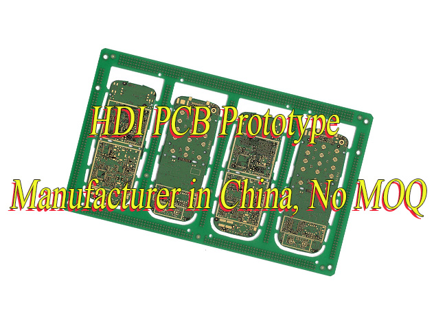
ELIC PCB means Every Layer Interconnect PCB. It is an advanced HDI PCB structure that uses laser microvias, copper-filled vias, and layer-to-layer interconnection to support compact, high-density electronic products. Compared with standard multilayer PCB or basic HDI PCB, ELIC PCB gives engineers more routing space in a smaller board area.

EBest Circuit (Best Technology) supports ELIC PCB and advanced HDI PCB projects through DFM review, manufacturability review, PCB layout support based on customer-provided inputs, PCB fabrication, PCBA assembly, component sourcing, testing coordination, and production traceability. We do not provide full circuit design, RF design, or product design services. Our role is to help customers turn approved design inputs into manufacturable and production-ready PCB/PCBA projects. For engineering review or quotation support, please send your Gerber files, stack-up, BOM, drawings, and project requirements to sales@bestpcbs.com.

ELIC PCB

What Is ELIC PCB?

ELIC PCB is a high-end HDI board where different layers can be connected through laser-drilled and copper-filled microvias. It is also commonly called any-layer HDI PCB.

In simple terms:

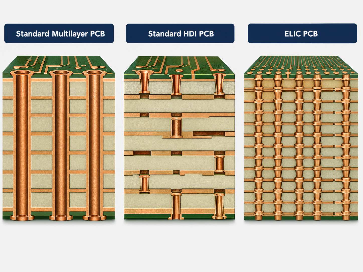
  • Standard multilayer PCB mainly uses through holes.
  • Standard HDI PCB uses blind vias, buried vias, and microvias in selected layers.
  • ELIC PCB allows high-density interconnection across layers with filled microvias.
ELIC PCB

The real value of ELIC PCB is not just β€œmore layers.”
It is more routing freedom in less space.

ELIC PCB is usually used when a product needs:

  • compact board size;
  • high component density;
  • fine-pitch BGA fanout;
  • short signal paths;
  • thinner PCB structure;
  • stable high-speed signal routing;
  • high-reliability interconnection;
  • more functions in limited space.

A typical ELIC PCB may include:

  • laser microvias;
  • stacked microvias;
  • copper-filled microvias;
  • via-in-pad structures;
  • fine line and spacing;
  • multiple lamination cycles;
  • high-density routing between layers.

For customers, the key question is not only β€œWhat is ELIC PCB?”
The more practical question is:

Can the manufacturer control microvia quality, copper filling, lamination, registration, testing, and assembly readiness?

That is where a precision ELIC PCB manufacturer becomes important.

What Is the ELIC PCB Process?

The ELIC PCB process is more demanding than standard multilayer PCB manufacturing. It requires accurate laser drilling, copper filling, sequential lamination, and strict process control.

A simplified process includes:

  • Inner Layer Fabrication
    Inner copper layers are imaged, etched, inspected, and prepared for lamination.
  • Lamination
    Core materials and prepregs are pressed together under controlled temperature and pressure.
  • Laser Microvia Drilling
    Small microvias are drilled by laser between adjacent layers.
  • Microvia Metallization
    The laser-drilled holes are cleaned and prepared for copper deposition.
  • Copper-Filled Microvias
    Microvias are filled with copper to support stacked or any-layer interconnection.
  • Sequential Build-Up
    Additional layers are built step by step. Each cycle needs alignment, lamination, drilling, plating, and inspection.
  • Outer Layer Imaging and Etching
    Final outer circuits are formed after the internal structures are completed.
  • Surface Finish
    ENIG, ENEPIG, OSP, immersion silver, or other finishes may be selected based on assembly and reliability needs.
  • Inspection and Testing
    AOI, electrical testing, X-ray, impedance testing, and microsection inspection may be required.

For ELIC PCB, the main manufacturing risks often come from:

  • microvia reliability;
  • copper filling quality;
  • stacked via alignment;
  • layer-to-layer registration;
  • multiple lamination control;
  • fine line and spacing control;
  • board thickness control;
  • impedance consistency;
  • warpage control;
  • SMT assembly yield.

EBest Circuit (Best Technology) can review customer files before production and check manufacturability risks related to microvias, stack-up, pad structure, surface finish, and assembly requirements.

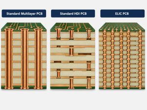
ELIC PCB vs Standard HDI PCB: What Is the Difference?

ELIC PCB belongs to the HDI PCB family, but it is more advanced than many standard HDI structures.

PCB TypeMain StructureTypical Use
Standard Multilayer PCBMainly through holesGeneral electronics
Standard HDI PCBBlind vias, buried vias, selected microviasCompact electronics
ELIC PCBAny-layer interconnect with filled microviasHigh-density advanced electronics

The main difference is interconnection freedom.

Standard HDI PCB may use structures such as:

  • 1+N+1 HDI;
  • 2+N+2 HDI;
  • blind vias;
  • buried vias;
  • local microvias.

ELIC PCB goes further. It allows dense interconnection between layers through filled microvias, helping the board achieve a more compact layout.

This structure can help:

  • reduce PCB size;
  • shorten signal paths;
  • support fine-pitch BGA components;
  • improve routing efficiency;
  • reduce through-hole occupation;
  • allow more functions in a smaller board area.

However, ELIC PCB also increases manufacturing difficulty. Compared with standard HDI PCB, it needs stronger control over:

  • laser drilling;
  • microvia copper filling;
  • lamination cycles;
  • layer registration;
  • stacked via reliability;
  • inspection and testing.

ELIC PCB should be selected when the design truly needs high-density routing, miniaturization, or any-layer interconnection. If a standard HDI PCB can meet the product requirement, ELIC may not be necessary.

Where Is ELIC PCB Used?

ELIC PCB is used when products need high density, small size, short interconnect paths, and reliable performance.

Common applications include:

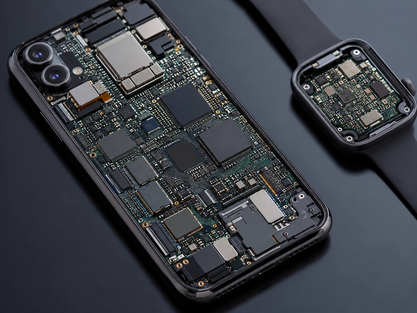
  • Smartphones and Wearable Devices
    These products need very small PCBs with high component density. ELIC helps save board space while supporting complex routing.
  • Camera Modules
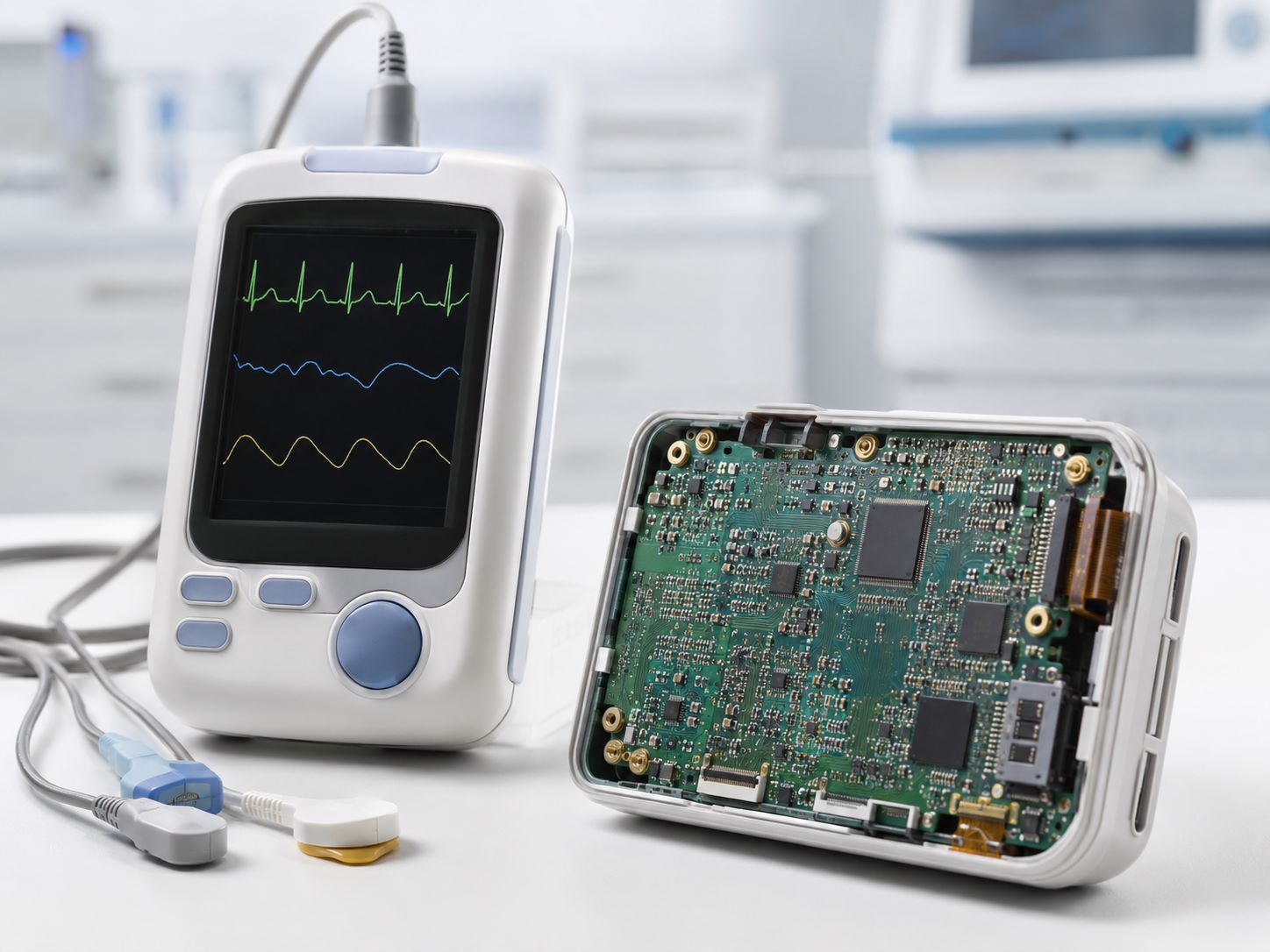
    Camera modules often use fine-pitch components and compact interconnection structures.
  • Medical Electronics
    Portable monitors, diagnostic modules, and compact medical devices may use advanced HDI structures to save space and improve assembly density.
  • Communication Modules
    High-density communication boards may need short signal paths, controlled routing, and stable interconnection.
  • High-Density Sensor Modules
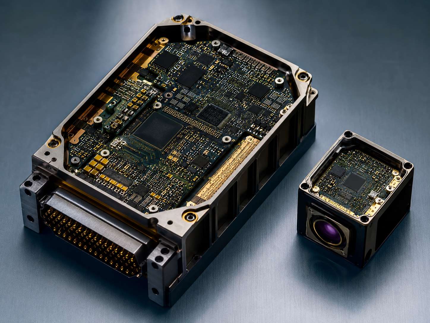
    Sensor products often combine small packages, limited board space, and strict connection reliability.
  • Aerospace Electronics
    Some aerospace modules need compact structure, weight reduction, and high-reliability interconnection.
  • Miniaturized Industrial Electronics
    Industrial modules are becoming smaller while still requiring stable performance and long service life.
  • Advanced Consumer Electronics
    Thin, compact devices with fine-pitch ICs and dense assembly may require ELIC PCB or advanced HDI PCB.

ELIC PCB is not used for every product. It is most valuable when ordinary multilayer PCB or standard HDI PCB cannot provide enough routing space or interconnection flexibility.

Case Study: ELIC PCB Manufacturing from EBest Circuit (Best Technology)

This case is based on a representative ELIC PCB manufacturing scenario from EBest Circuit (Best Technology). Customer details and product information are generalized to protect confidentiality, while the board specifications are presented in a practical format for engineers and buyers.

Project Overview

The project required an 8-layer ELIC FR4 PCB for a compact high-density electronic module. The board needed any-layer interconnection, laser microvias, copper-filled vias, BGA via-in-pad, controlled impedance, and SMT-ready panel delivery.

This was not a standard HDI board. The key requirement was to create reliable interconnection between adjacent layers while keeping the PCB thin, dense, and suitable for fine-pitch component assembly.

Customer Requirements

The customer needed a compact PCB with:

  • 8-layer any-layer HDI structure;
  • laser microvias between adjacent layers;
  • copper-filled microvias;
  • BGA via-in-pad with resin filling and planarization;
  • controlled impedance with impedance report;
  • black solder mask and white silkscreen;
  • ENIG 1u” surface finish;
  • panel delivery with 3 Mark points for SMT assembly.

The project required close control of microvia reliability, layer registration, copper filling, impedance, pad flatness, and SMT assembly readiness.

EBest Circuit (Best Technology)’s Support

EBest Circuit (Best Technology) reviewed the customer-provided files from a manufacturability perspective before production.

Our support focused on:

  • DFM review;
  • ELIC stack-up manufacturability review;
  • laser microvia and copper filling process review;
  • via-in-pad resin filling and planarization control;
  • controlled impedance manufacturing;
  • SMT panel optimization;
  • electrical testing and impedance report;
  • PCBA assembly readiness review.

Where layout adjustment was needed, EBest Circuit (Best Technology) supported PCB layout work based on the customer’s approved design inputs. This was layout support, not full circuit design, RF design, or product design.

Project Result

The project was completed as an 8-layer ELIC PCB with any-layer interconnect structure. The board supported fine-pitch BGA assembly, controlled impedance, and SMT-ready panel delivery.

This case shows why ELIC PCB manufacturing depends on more than layer count. Microvia structure, copper filling, lamination control, impedance, surface finish, and assembly preparation must be reviewed together before production.

Case Board Specifications

ItemSpecification
PCB Type8L ELIC FR4 PCB / Any-Layer HDI PCB
MaterialHigh-Tg FR4, Tg 170Β°C
Finished Thickness0.97mm
Copper Weight0.5oz
Interconnect StructureEvery Layer Interconnect
Microvia StructureAdjacent-layer laser microvias from L1-L2 to L7-L8
Via ProcessCopper-filled laser microvias
Minimum Microvia Size0.1mm
BGA AreaVia-in-pad with resin filling and planarization
Surface FinishENIG 1u”
Solder Mask / SilkscreenBlack solder mask, white silkscreen
Impedance Control50Ξ© single-ended, 90Ξ© / 100Ξ© differential impedance
SMT Delivery RequirementPanel delivery with 3 Mark points on the panel edge
Testing RequirementElectrical test and impedance report

Top 10 ELIC PCB Manufacturer Supplier Reference in China

The following list is not an official ranking. It is a supplier reference for customers comparing ELIC PCB, any-layer HDI PCB, and advanced HDI PCB manufacturing options in China. Before selecting a supplier, customers should still confirm the real project details, including microvia structure, copper filling, layer count, line width and spacing, stack-up, testing requirements, assembly needs, and production volume.

CompanyCompany Positioning
EBest Circuit (Best Technology)Engineer-oriented one-stop PCB and PCBA service provider
Avary HoldingLarge-scale HDI PCB manufacturer
DSBJ / MultekHigh-end interconnect PCB manufacturer
WUS Printed CircuitHigh-speed and HDI PCB manufacturer
KinwongAutomotive and HDI PCB manufacturer
Shengyi ElectronicsHigh-reliability HDI PCB manufacturer
Suntak TechnologyMultilayer and HDI PCB supplier
MADPCBPrototype-to-production HDI PCB supplier
WellPCBOnline HDI PCB manufacturing service provider
PCBWayOnline prototype and small-batch PCB platform

This supplier reference can help customers build an initial shortlist. However, ELIC PCB projects should not be sourced only by company size or website claims. A better way is to ask whether the supplier can support the exact ELIC structure in your files, including laser microvias, stacked vias, copper filling, sequential lamination, impedance control, inspection, and PCBA assembly if required.

For customers who need both advanced PCB manufacturing and assembly support, EBest Circuit (Best Technology) can provide DFM review, PCB layout support based on customer inputs, ELIC/HDI PCB fabrication, PCBA assembly, component sourcing, testing coordination, and MES-based production traceability. This makes the project easier to manage from prototype validation to batch production.

Why Choose EBest Circuit (Best Technology) as Your ELIC PCB Manufacturer?

Choosing an ELIC PCB manufacturer is not only about finding a PCB factory. It is about finding a team that understands the manufacturing risks behind advanced HDI structures.

EBest Circuit (Best Technology) supports customers in several practical areas.

ELIC and HDI PCB Manufacturing Support

We can support advanced PCB projects involving:

  • ELIC PCB;
  • any-layer HDI PCB;
  • multilayer HDI PCB;
  • blind and buried vias;
  • laser microvias;
  • copper-filled microvias;
  • via-in-pad structures;
  • fine line and spacing;
  • high-density BGA breakout.

DFM Review

Before production, EBest Circuit (Best Technology) can review:

  • Gerber files;
  • stack-up;
  • via structure;
  • annular ring;
  • line width and spacing;
  • solder mask clearance;
  • copper balance;
  • surface finish;
  • panelization;
  • testing requirements.

This helps reduce avoidable manufacturing risks before the board enters production.

PCB Layout Support Based on Customer Inputs

EBest Circuit (Best Technology) can support PCB layout work when the customer provides the required inputs, such as:

  • schematic;
  • netlist;
  • component placement requirements;
  • mechanical outline;
  • connector locations;
  • impedance requirements;
  • routing rules;
  • keep-out areas;
  • assembly requirements.

Our role is to prepare or adjust manufacturable PCB layout files based on customer-provided design inputs. We do not position this as full PCB design, circuit design, RF design, or product design.

PCB Fabrication and PCBA Assembly

Many ELIC PCB projects also require assembly support. EBest Circuit (Best Technology) can support:

  • PCB fabrication;
  • component sourcing;
  • SMT assembly;
  • through-hole assembly;
  • assembly process review;
  • AOI inspection;
  • X-ray inspection when needed;
  • electrical testing;
  • functional testing coordination.

Quality and Traceability

For high-reliability projects, documentation and traceability matter.

EBest Circuit (Best Technology) can support:

  • production quality records;
  • incoming material control;
  • process tracking;
  • MES-based traceability;
  • inspection records;
  • testing coordination;
  • prototype to batch production support.

Industry Support

Our PCB and PCBA services are suitable for projects in:

  • medical electronics;
  • industrial control;
  • communication equipment;
  • automotive electronics;
  • aerospace electronics;
  • sensor modules;
  • compact electronic devices;
  • high-density electronic assemblies.

If your project needs ELIC PCB manufacturing, HDI PCB fabrication, or PCBA assembly support, send Gerber files, stack-up, BOM, drawings, and requirements to sales@bestpcbs.com. As an advanced HDI PCB manufacturer, EBest Circuit (Best Technology) can review manufacturability, production feasibility, assembly needs, and quotation details.

FAQs About ELIC PCB

1. What does ELIC PCB mean?
ELIC PCB means Every Layer Interconnect PCB. It is an advanced HDI PCB structure that allows high-density interconnection across layers through laser microvias, usually with copper filling.

2. Is ELIC PCB the same as HDI PCB?
ELIC PCB belongs to the HDI PCB family, but it is more advanced than many standard HDI structures. It is often understood as any-layer HDI PCB.

3. What is the main advantage of ELIC PCB?
The main advantage is high-density interconnection in a compact board area. It helps reduce board size, improve routing freedom, and support fine-pitch components.

4. Does ELIC PCB use laser microvias?
Yes. ELIC PCB usually uses laser-drilled microvias, and these microvias are often copper-filled to support stacked interconnect structures.

5. Is ELIC PCB more expensive than standard HDI PCB?
Usually yes. ELIC PCB requires more complex processes, such as laser drilling, copper filling, sequential lamination, tighter registration control, and more inspection.

6. What products use ELIC PCB?
ELIC PCB is used in compact and high-density electronics, such as smartphones, wearable devices, camera modules, medical electronics, communication modules, sensor modules, aerospace electronics, and advanced consumer electronics.

7. What files are needed for an ELIC PCB quotation?
Customers should provide Gerber files, stack-up, drill files, fabrication drawing, BOM if assembly is needed, impedance requirements, board thickness, copper thickness, surface finish, testing requirements, and application notes if available.

8. Can EBest Circuit (Best Technology) provide PCB design for ELIC PCB projects?
EBest Circuit (Best Technology) does not provide full PCB design, circuit design, RF design, or product design services. We can support PCB layout work when the customer provides complete design inputs, and we can provide DFM review for PCB fabrication and assembly.

9. Can EBest Circuit (Best Technology) support ELIC PCB fabrication and assembly?
Yes. EBest Circuit (Best Technology) can support ELIC/HDI PCB manufacturability review, PCB fabrication, PCBA assembly, component sourcing, testing coordination, and production traceability.

10. How can I get an ELIC PCB quotation?
Send your Gerber files, stack-up, BOM, drawings, and project requirements to sales@bestpcbs.com. EBest Circuit (Best Technology) will review manufacturability, assembly needs, testing requirements, and quotation details.

ELIC PCB is a manufacturing-intensive structure that requires strong process control. Microvia reliability, copper filling, layer registration, lamination control, testing, and assembly support all affect the final result. EBest Circuit (Best Technology) supports ELIC PCB and advanced HDI PCB projects from DFM review to PCB fabrication, PCBA assembly, testing, and production traceability. For engineering review or quotation support, please send your Gerber files, stack-up, BOM, drawings, and project requirements to sales@bestpcbs.com.

You may also like

Rigorous Quality RF HDI Circuit Board Manufacturer from Prototypes to Assembly
Tuesday, March 31st, 2026

RF HDI circuit board is the critical foundation for high-frequency, high-speed electronics, merging the signal integrity of radio frequency designs with the dense interconnects of HDI technology. This article provides a comprehensive guide to RF HDI boards, addressing key design challenges and showcasing how a manufacturer with full turnkey capabilities ensures success from prototype to final assembly.

Engineers and procurement specialists often face significant hurdles when sourcing advanced RF HDI circuit boards. Common pain points include:

  • Struggling to find a manufacturer capable of handling ultra-fine features like 3.3-mil flip-chip pitch.
  • Experiencing inconsistent quality or outright rejection from suppliers lacking advanced HDI processes.
  • Facing long lead times and poor communication, especially with offshore suppliers that can’t support rapid iteration.
  • Dealing with the complexity of managing separate vendors for RF PCB fabrication and assembly.
  • Receiving inadequate DFM feedback, resulting in designs that are difficult or costly to manufacture.

At EBest Circuit (Best Technology), we resolve these challenges through our integrated, expert-driven approach. Our solutions are built on:

  • Proven Advanced Process Capability:​ Expertise in HDI PCB manufacturing​ with 3/3 mil line/space and 4 mil laser micro-drilling.
  • Full In-House Control:​ A true one-stop service encompassing design, advanced packaging substrate manufacturing, fabrication, and assembly under rigorous quality systems.
  • Rapid and Reliable Execution:​ Dedicated engineering support and a 24-hour rapid prototyping service to accelerate your development cycle.
  • Turnkey Simplification:​ A seamless supply chain from component sourcing to final box build, managed by a single point of contact.
  • Collaborative Engineering Partnership:​ Proactive Design for Manufacturability (DFM)​ analysis to optimize your fine-pitch flip-chip assembly​ and RF performance before production begins.

Founded in 2006, EBest Circuit (Best Technology) is a certified, full-service PCB and PCBA manufacturer with two decades of specialization in high-technology circuit boards. We operate a 28,900 sq. meter facility equipped with state-of-the-art machinery, from CNC laser drills for high-density via PCB​ creation to advanced SMT lines for precision assembly. Holding certifications like ISO 9001:2015, IATF 16949, and ISO 13485:2016, we serve over 1,700 clients across 40+ countries with a 97% on-time delivery rate. Our core strength lies in transforming complex RF and HDI designs into reliable, high-performance products. For a consultation on your next project, pls feel free to contact us at sales@bestpcbs.com.

RF HDI Circuit Board

What Is An RF HDI Circuit Board?

An RF HDI circuit board is a sophisticated printed circuit board designed to operate at high frequencies (typically from hundreds of MHz to several GHz) while incorporating High-Density Interconnect (HDI) technology. It combines the need for controlled impedance, low signal loss, and minimal electromagnetic interference of RF design with the space-saving, high-performance interconnects of HDI, which uses micro-vias, fine lines, and multiple via-in-pad structures. This convergence is essential for modern compact, high-speed devices like 5G infrastructure, advanced radar systems, and high-frequency test equipment.

Key characteristics include:

  • Advanced Materials:​ Use of low-loss, stable dielectric substrates like Rogers RO4350B or Taconic, rather than standard FR4.
  • Micro-Via Technology:​ Extensive use of blind, buried, and stacked micro-vias (as small as 4 mils in diameter) to facilitate dense routing.
  • Fine Features:​ Trace/space widths down to 3/3 mils to accommodate fine-pitch ICs and complex routing.
  • Impedance Control:​ Tightly controlled dielectric thickness and trace geometry to maintain specific impedance values (e.g., 50Ξ©, 100Ξ© differential).
  • Thermal Management:​ Strategic placement of thermal vias and use of materials with appropriate thermal conductivity to dissipate heat from active components.

In summary, an RF HDI board is the enabling platform for electronics where signal speed, integrity, and component density are all paramount, requiring a manufacturer with precise process control and material expertise.

RF HDI Circuit Board

What Is the Difference Between RF and HDI Circuit Boards?

While both RF and HDI PCBs represent advanced circuit board technologies, they prioritize different design and performance goals. Understanding their distinctions is crucial for selecting the right board for your application and the right manufacturer for your project.

FeatureRF Circuit BoardHDI Circuit BoardRF HDI Circuit Board
Primary FocusHigh-frequency signal performanceHigh wiring densityHigh-frequency performance + high density
Typical MaterialLow-loss laminatesFR4 / high-performance FR4Low-loss laminates
Main ChallengeImpedance and dielectric loss controlMicrovia and fine-line reliabilityImpedance control + microvia reliability
Common FeaturesControlled impedance, ground isolationBlind/buried vias, via-in-padFine-pitch layout, via-in-pad
Process FocusMaterial consistencyLaser drilling, sequential laminationCombined RF + HDI process control

RF Boards​ focus on the “quality” of the signal path, minimizing loss and distortion. HDI Boards​ focus on the “quantity” and efficiency of connections, packing more functionality into less space. An RF HDI Board, the subject of this article, demands expertise in both domains, making the choice of manufacturerβ€”one like EBest Circuit with proven capability in both RF PCB manufacturing​ and HDI PCB manufacturingβ€”critical to success.

How Many Ground Vias Can Fit Under a Component?

Maximizing ground vias under a component, especially an RF die or a BGA, is vital for providing a low-inductance path to ground, improving thermal dissipation, and shielding. The quantity is determined by a combination of your design rules and the manufacturer’s fabrication limits.

The number is primarily constrained by:

  • Via Diameter and Pitch:​ Our standard micro-drilling capabilities​ allow for laser-drilled micro-vias as small as 4 mils (0.1mm) in diameter. The minimum via-to-via spacing (pitch) is typically 8-10 mils for these micro-vias. A smaller diameter and tighter pitch allow for more vias.
  • Pad Size:​ The component pad size sets the available real estate. Using a via-in-pad design is most effective.
  • Aspect Ratio:​ For thicker boards, the aspect ratio (board thickness to hole diameter) of mechanically drilled vias becomes a limiting factor. Our advanced capability allows an aspect ratio of up to 10:1 for reliable plating.

Illustrative Example:

Under a 1mm x 1mm (40 mil x 40 mil) flip-chip bump pad, assuming a 4 mil via diameter and a 10 mil via pitch (center-to-center), you could theoretically fit a 3×3 array of vias, totaling 9 ground vias. Our engineers can work with you to model the optimal via pattern and quantity to meet both electrical and thermal goals without compromising pad integrity.

What Are the Micro-Drilling Capabilities for RF HDI Boards?

Our micro-drilling capabilities​ are foundational to producing reliable high-density via PCBs​ and are a key differentiator for RF HDI work. We employ both mechanical and laser drilling technologies to achieve the precise, small-diameter holes required.

Our key specifications include:

Drilling TypeMinimum DiameterPrimary ApplicationNotes
Mechanical Drilling​8 mils (0.2mm)Through-holes, larger viasStandard process for most PTH.
Advanced Mechanical Drilling​6 mils (0.15mm)High-density through-holesUsed for more demanding designs.
Laser Drilling​4 mils (0.1mm)HDI micro-vias​ (blind/buried)Essential for fine-pitch flip-chip assembly​ and via-in-pad.

Supporting Infrastructure:

  • Equipment:​ We utilize advanced CNC laser drill machines to ensure clean, consistent micro-via formation.
  • Plating:​ Our automated plating lines (PTH & PPL) are calibrated to achieve excellent copper deposition in these high-aspect-ratio micro-vias, with a PTH wall thickness of 0.48 mils (12 Β΅m) for HDI designs.
  • Inspection:​ Micro-section analysis is routinely used to verify the quality and plating integrity of micro-vias, ensuring reliability.

Copper Fill vs. Resin Fill: Which Is Better for Vias?

Choosing between copper-filled and resin-filled vias depends on the primary design objective: electrical/thermal performance or surface planarization.

CriteriaCopper-Filled ViasResin-Filled Vias
Main PurposeHeat transfer and conductivitySurface leveling
Thermal PerformanceExcellentLow
Electrical ConductivityConductiveNon-conductive
Surface FlatnessGood, may need extra planarizationExcellent
Typical UsePower and RF thermal areasFine-pitch BGAs
CostHigherLower

Our Recommendation:

For RF HDI designs​ where thermal management under the die is a priorityβ€”exactly as highlighted in the client’s requestβ€”copper-filled vias are typically the better choice. We can efficiently fill laser micro-vias with copper to create effective thermal conduits. For designs where absolute surface flatness is the overriding concern for solder joint reliability, resin fill is the appropriate option. Our engineering team can advise on the best approach during the DFM review.

Can RO4350B Support High-Density RF Designs?

Yes, absolutely. Rogers RO4350B is an excellent laminate choice for high-density RF designs​ and is a material we routinely process. It strikes a optimal balance between RF performance and manufacturability, making it suitable for RF HDI circuit boards.

Why RO4350B is suitable for HDI:

  • Process Compatibility:​ Unlike pure PTFE materials, RO4350B is a ceramic-filled hydrocarbon laminate. It has a modifiable surface and can be processed using manufacturing methods similar to FR4, making it compatible with the sequential lamination and laser drilling processes required for HDI.
  • Dimensional Stability:​ It exhibits good dimensional stability, which is crucial for the layer-to-layer registration accuracy needed in multi-layer HDI stack-ups.
  • Consistent Dielectric Constant:​ Its stable Dk (3.48) and low dissipation factor (0.0037) across a wide frequency range ensure predictable impedance and low signal loss in dense designs.

Our Experience with RO4350B:

Our RF board​ capabilities explicitly list Rogers materials like RO4350B. We handle the specific challenges of these materials, such as ensuring proper hole wall preparation for reliable plating in PTHs. We can fabricate boards with RO4350B across a thickness range of 0.5mm to 3.0mm, supporting various advanced packaging substrate manufacturing​ needs.

How to Scale RF HDI Designs from Prototype to Production?

Scaling an RF HDI design from a few prototypes to volume production requires careful planning and a manufacturer with scalable processes and a robust supply chain. Here is a structured approach:

  • Prototype with Production in Mind:​ Engage with your manufacturer’s engineering team early. Our DFM analysis for prototypes will flag any features (e.g., ultra-tight tolerances, exotic materials) that may be costly or risky to scale.
  • Qualify the Manufacturing Process:​ Use the prototype phase to not just test the board’s function, but also to audit the manufacturer’s quality. We provide micro-section reports and test data, establishing a quality baseline for production.
  • Lock Down Materials and Parameters:​ Finalize the bill of materials (BOM) for the laminate, prepreg, and surface finish. Document all critical process parameters established during prototyping.
  • Plan for Test Fixturing:​ Prototypes are often tested with flying probes. For volume production, design and procure dedicated test fixtures (e.g., bed-of-nails) during the prototyping lead time to avoid delays.
  • Implement Statistical Process Control (SPC):​ In production, we monitor key parameters (e.g., impedance, copper thickness) using SPC charts to detect and correct process drift before it causes defects.
  • Leverage the Manufacturer’s Volume Capacity:​ Our monthly production capacity of 260,000 square feet is designed to absorb volume orders without sacrificing the lead time or quality standards set during prototyping.

How to Ensure Reliability in Advanced Packaging Substrates?

Ensuring reliability in advanced packaging substratesβ€”a category that includes complex RF HDI boardsβ€”requires a holistic approach focused on material science, process control, and rigorous testing.

Our reliability assurance framework is built on four pillars:

  1. Material Selection and Compatibility:​ We ensure all materials in the stack-up (core, prepreg, copper, solder mask) have matched coefficients of thermal expansion (CTE) as closely as possible to minimize stress during thermal cycling. We only source materials from qualified, certified suppliers.
  2. Robust Process Engineering:
    • Desmear and Plating:​ For HDI micro-vias, we employ optimized plasma desmear and electrolytic plating processes to ensure a void-free, high-integrity copper connection, critical for thermal and electrical reliability.
    • Lamination Control:​ Precise control of lamination pressure, temperature, and vacuum is maintained to prevent delamination.
  3. Comprehensive Inspection and Testing:
    • Electrical Testing:​ 100% electrical test (using flying probe or fixture) for continuity and isolation.
    • Automated Optical Inspection (AOI):​ For detecting surface defects on inner and outer layers.
    • Micro-sectional Analysis:​ Destructive cross-sectioning to verify via plating quality, layer alignment, and interlayer bonding.
    • Reliability Stress Testing:​ We can perform thermal shock, thermal cycling, and highly accelerated life testing (HALT) on samples to validate product lifetime under simulated operating conditions.
  4. Certification and Standards Adherence:​ Our production follows IPC-6012 Class 2/3 standards for rigid boards and IPC-6013 for flex circuits. Our ISO 9001, ISO 13485, IATF 16949, AS9100D certifications mandates a process-focused approach to defect prevention and continuous improvement, inherently boosting long-term reliability.
RF HDI Circuit Board

To sum up, RF HDI circuit boards​ are the sophisticated engines powering the next generation of high-frequency, miniaturized electronics. This article has explored their defining characteristics, key manufacturing considerations, and the path from prototyping to reliable production.

Choosing the right partner is paramount. EBest Circuit (Best Technology) combines 20 years of precision manufacturing expertise with a full turnkey service model. From handling your 3.3-mil flip-chip pitch and high-density via PCB​ challenges to providing expert DFM on your advanced packaging substrate​ design, we ensure rigorous quality at every stepβ€”from the initial prototype to volume assembly.

Pls feel free to contact our engineering sales team anytime at sales@bestpcbs.com​ for a comprehensive quote and DFM analysis.

FAQs About RF HDI Circuit Board

Q: Can Your PCB Supplier Handle 3.3-mil Flip-Chip Pitch?

A: Yes, we can. Handling a 3.3-mil (approx. 0.084mm) flip-chip pitch is a demanding but achievable requirement that falls under our HDI and advanced packaging​ capabilities. It requires our most precise laser drilling for micro-vias (4 mil) and expert solder mask control to define such fine pad separations. Success depends on a collaborative DFM review to optimize the pad design, solder mask dam, and via-in-pad structure. We have the equipment and process expertise to support this level of fine-pitch flip-chip assembly.

Q: What is your minimum line width/space for HDI designs?

A: For our advanced HDI process, our standard minimum line width and space is 3/3 mils (0.075/0.075mm). This capability is clearly listed in our FR4 PCB capability table under the “HDI” specification and is essential for routing the escape patterns from fine-pitch components used in RF HDI circuit boards.

Q: What impedance control tolerance can you achieve?

A: We offer tight impedance control for RF designs. For impedance values greater than 50Ξ©, we maintain a tolerance of Β±10%. For values of 50Ξ© or less, we control to within Β±5Ξ©. This is achieved through precise control of dielectric thickness, etch profile, and material selection, such as Rogers RO4350B.

Q: What is your standard and fastest lead time for an RF HDI prototype?

A: Lead time depends on layer count and complexity. For a standard specification 4-layer FR4-based prototype, our normal service is 10 days, with a 48-hour fastest service. For RF boards​ using specialized materials like Rogers, the typical sample lead time is 7-9 days. We always recommend contacting us with your Gerber files for the most accurate quote and expedited options.

You may also like

HDI PCB Manufacturing, 3 Step HDI PCB Manufacturer
Tuesday, October 21st, 2025

HDI PCB manufacturing​ is a specialized process that pushes the boundaries of electronics design. It allows for the creation of incredibly complex and powerful devices that fit in the palm of your hand. This blog explains the process, benefits, and how to choose the right manufacturer for your advanced projects.

Are you battling with signal integrity issues in your HDI PCB designs? Many engineers and product managers face these exact challenges when pushing their PCB HDI technology forward.

  • ​Difficulty achieving high component density​ in a limited board space.
  • ​Signal loss and interference​ in complex, high-speed designs.
  • ​Managing heat dissipation​ in increasingly powerful but compact devices.
  • ​Facing high costs and long lead times​ for sophisticated multi-layer boards.
  • ​Finding a manufacturer with the right expertise and technology​ to bring an advanced design to life.

The good news is that these challenges have right solutions. By partnering with a skilled manufacturer, you can overcome these obstacles. Here is how a professional ​HDI PCB manufacturer​ addresses these points:

  • Utilizing microvias and stacked vias to maximize routing density in a small area.
  • Implementing precise impedance control and advanced materials to ensure clean signal transmission.
  • Offering specialized materials and thermal management techniques to keep your device running cool.
  • Providing cost-effective manufacturing strategies and reliable quick-turn services to meet your timeline and budget.
  • Bringing years of specialized experience and state-of-the-art equipment like laser drilling machines to the table.

BEST Technology is a professional ​HDI PCB manufacturing​ factory focused on delivering high-quality, high-density interconnect solutions. Our team is dedicated to supporting your projects from the initial design review to final assembly. For a personal consultation, pls feel free to reach out to us at sales@bestpcbs.com.

HDI PCB Manufacturing

​What Is HDI PCB Manufacturing?​​

At its heart, ​HDI PCB manufacturing​ is all about packing more functionality into a smaller space. It’s the advanced process of creating printed circuit boards with a significantly higher wiring density per unit area than conventional PCBs. Think of it as the difference between a wide, sprawling suburban neighborhood and a dense, efficient city skylineβ€”both serve a purpose, but one is built for maximum space efficiency and interconnection.

To truly grasp the ​HDI PCB meaning, it’s helpful to understand its key building blocks:

  • ​1. Microvias, Blind, Buried and Through Vias:​​ These are the tiny, laser-drilled holes that make HDI possible.
    • ​Microvias​ are incredibly small holes, typically with a diameter of less than 0.15mm. They act as miniature tunnels connecting adjacent layers.
    • ​Blind Vias​ connect an outer layer to an inner layer, but don’t go all the way through the board.
    • ​Buried Vias​ connect inner layers only, remaining hidden within the board’s core.
    • Through-holes refer to a hole that is open on both outer layers of a PCB, thereby connecting the two sides. This term encompasses via holes, plated through-holes (PTH), and non-plated through-holes (NPTH).
    • ​Why they matter:​​ By using these small, targeted vias instead of large through-holes, designers can save a tremendous amount of space. This freed-up real estate allows for more components and more complex routing.
  • ​2. The Evolution to UHDI (Ultra High Density Interconnect):​​ As technology pushes for even greater miniaturization, ​UHDI​ represents the next frontier. It involves even finer lines, smaller vias, and more advanced materials. If HDI is a dense city, UHDI is a city of micro-skyscrapers.
  • ​3. The Role of a Specialized HDI PCB Manufacturer:​​ Not every factory can produce these advanced boards. A specialized ​HDI PCB manufacturer​ invests in specific technologyβ€”like laser drilling systemsβ€”and cultivates the expertise needed to manage the complex, sequential lamination processes involved. Choosing the right partner is crucial for success.

To truly understand what HDI PCBs are, let’s look at their key characteristics:

​Key Features of HDI Technology:​​

  • Uses laser drilling instead of mechanical drilling, with via diameters ≀0.15mm
  • Microvias with bottom pads smaller than 0.25mm (10mil)
  • Fine line width/spacing of 3/3mil or less
  • Requires copper plating thickness β‰₯15ΞΌm in laser vias
  • Aspect ratio (dielectric thickness to via diameter) ≀1:1

​How HDI Differs from Standard PCBs:​​

  1. Contains blind vias, buried vias, or both
  2. Requires multiple lamination cycles (β‰₯2 times)
  3. Involves multiple drilling and plating processes
  4. Features much denser routing on both inner and outer layers
  5. Has more complex manufacturing process and longer production cycles

In short, ​HDI PCB manufacturing​ is the enabling technology behind the powerful, compact electronics we rely on every day.

​What Are the Types of HDI PCB Manufacturing Products?​​

​The world of HDI is diverse, offering solutions for many different applications. The types of products are primarily classified by their layer buildup structure, which refers to the number of sequential lamination cycles and the arrangement of microvias. Understanding these structures is key to selecting the right board for your project.

A crucial concept here is the “order” or “step” of an HDI board, often described by formulas like ​a+N+a​ or ​a+N+N+a.

  • ​a​ stands for the ​Build-up layer, which is formed using laser microvias. Each additional build-up layer on one side counts as one “step” or “order”.
  • ​N​ stands for the ​Core layer, which is a traditional multilayer PCB with through-holes or buried vias. The value of N indicates the number of conductive layers within the core. For example, a 4-layer core is N=2 (counting internal layers), and an 8-layer core is N=4. This explains why “N” is often an even number.

Here is a clear outline of common HDI structures, from simple to complex:

​1. 1+N+1 (1-Step HDI)​​

This is the simplest form of HDI. It features a single build-up of high-density interconnection layers on both sides of a core. This is a cost-effective entry point for adding HDI features, allowing for finer lines and microvias while keeping the process relatively straightforward.

HDI PCB Manufacturing

​2. 2+N+2 (2-Step HDI)​​

This structure involves two sequential HDI build-ups on each side. This allows for the use of stacked microvias (microvias placed directly on top of each other) or staggered microvias. It is ideal for designs requiring higher pin-count components and much greater routing density.

HDI PCB Manufacturing

​3. 3+N+3 and Beyond (3-Step / Any-layer HDI)​​

These are the most complex and advanced boards. They feature three or more sequential laminations, enabling “any-layer” interconnection, where virtually any layer in the board can be interconnected with microvias. This enables incredibly high component density and is used in cutting-edge applications like flagship smartphones, network servers, and medical imaging equipment.

HDI PCB Manufacturing

​HDI vs. Mechanical Blind/Buried Vias​

It’s important to distinguish between laser-drilled HDI microvias and mechanically drilled blind/buried vias, as they represent different product types with distinct cost and capability profiles.

  • ​HDI (Laser Drilled):​​
    • ​Microvia Aperture:​​ ≀ 0.15mm.
    • ​Characteristics:​​ Uses laser drilling for high positioning accuracy, enabling very small apertures. Employs RCC (Resin Coated Copper) or laser-specific prepreg as dielectric material.
    • ​Applications:​​ High-end miniaturized products.
  • ​Mechanical Blind/Buried Vias:​​
    • ​Aperture:​​ Typically β‰₯ 0.2mm.
    • ​Characteristics:​​ Uses mechanical depth-controlled drilling. Generally more cost-effective for larger diameter holes or high-volume production. Filled with resin or copper paste.
    • ​Applications:​​ Applications requiring inter-layer connections but not the ultimate density.

​Complex Structural Variations​

HDI technology allows for complex combinations to meet specific design needs, such as stacked microvias, staggered microvias, and mixed structures combining laser and mechanical vias. These advanced configurations provide maximum design flexibility for the most demanding applications.

​Beyond the Layer Count: Other HDI Product Forms​

Furthermore, HDI technology is applied across various product forms to meet specific application needs:

  • ​HDI Rigid-Flex PCB Boards:​​ Combine the durability of rigid boards with the flexibility of flexible circuits, using HDI technology to maximize density in the rigid sections and interconnection points.
  • ​Specialized High-Frequency HDI Boards:​​ Utilize advanced dielectric materials with low loss tangent, combined with HDI design rules, to ensure signal integrity in high-speed digital and RF applications.

The goal of all these HDI PCB manufacturing products is always the same: to pack more performance and functionality into a smaller, lighter, and more reliable package. Understanding these types and structures helps in selecting the optimal product for your project’s specific needs, balancing complexity, performance, and cost.

​What Is the Process of HDI PCB Fabrication?​​

The fabrication process for HDI PCBs is a highly precise and sequential operation that involves multiple cycles of lamination, drilling, and plating. This complex manufacturing process requires strict process controls and advanced equipment to achieve the high density interconnections characteristic of HDI boards. Here is the detailed manufacturing process of 3-Step HDI PCB:

​Stage 1: Core Layer Processing​

The foundation of HDI PCB starts with the core layer processing, which establishes the basic interconnection framework:

  1. ​Panel Cutting​ – The process begins with cutting the base copper-clad laminate to the required size for panel processing.
  2. ​Inner Layer Imaging​ – The circuit pattern is transferred to the core using photolithography with a dry film resist.
  3. ​AOI (Automated Optical Inspection)​​ – The imaged inner layer circuits are automatically inspected for defects like opens, shorts, or pattern irregularities.
  4. ​Lamination​ – Multiple inner layers are bonded together with prepreg under heat and pressure to form the core structure.
  5. ​Copper Reduction​ – Excess copper is chemically etched away to define the precise circuit traces.
  6. ​Laser Drilling​ – Microvias with diameters ≀0.15mm are ablated using a precision laser drill system.
  7. ​Mechanical Drilling​ – Through-holes are drilled mechanically for layer-to-layer connections.
  8. ​Electroless Copper Deposition​ – A thin conductive copper layer is chemically deposited onto the entire panel, including the walls of all drilled holes.
  9. ​Via Filling​ – The vias are filled with conductive paste or resin to create a flat surface for subsequent layers.

​Stage 2: First Build-Up Layer (2nd Lamination Cycle)​​

The first HDI build-up layer adds additional interconnection density:

  1. ​Inner Layer Imaging​ – Circuit pattern imaging for the first build-up layer using LDI (Laser Direct Imaging) for higher precision.
  2. ​AOI (Automated Optical Inspection)​​ – Comprehensive inspection of the imaged layer to ensure pattern accuracy.
  3. ​Lamination​ – The first build-up dielectric layer is laminated onto the core structure.
  4. ​Copper Reduction​ – Copper is etched to define the fine-line circuits on this layer.
  5. ​Laser Drilling​ – Second-level microvias are drilled for the first build-up layer interconnection.
  6. ​Electroless Copper Deposition​ – Copper deposition ensures proper conductivity in the new microvias.
  7. ​Via Filling​ – The newly drilled microvias are filled to maintain surface planarity.
  8. ​Inner Layer Imaging​ – Additional circuit patterning for complex routing requirements.
  9. ​AOI​ – Final inspection before proceeding to the next build-up layer.

​Stage 3: Second Build-Up Layer (3rd Lamination Cycle)​​

The second build-up layer further enhances the interconnection density:

  1. ​Lamination​ – The second build-up dielectric layer is laminated onto the existing structure.
  2. ​Copper Reduction​ – Precision etching defines the circuits on this critical layer.
  3. ​Laser Drilling​ – Third-level microvias are drilled with high positioning accuracy.
  4. ​Mechanical Drilling​ – Additional through-holes are drilled for final layer connections.
  5. ​Electroless Copper Deposition​ – Complete copper deposition ensures reliable conductivity.
  6. ​Via Filling​ – All microvias are properly filled to achieve the required surface flatness.

​Stage 4: Outer Layer Processing and Finalization​

The final stage completes the HDI PCB manufacturing:

  1. ​Outer Layer Imaging​ – The final circuit pattern is applied to the outer layers using high-precision LDI.
  2. ​Etching​ – Unwanted copper is precisely etched away from the outer layers.
  3. ​AOI (Automated Optical Inspection)​​ – Comprehensive final inspection of the completed circuitry.
  4. ​Solder Mask Application​ – A protective solder mask layer is applied to the outer surfaces.
  5. ​Silkscreen Printing​ – Identifying text, logos, and component symbols are printed.
  6. ​Surface Finish (ENIG/ENEPIG)​​ – A final surface finish is applied for solderability and protection.
  7. ​Profile Routing​ – Individual boards are routed out of the production panel.
  8. ​Electrical Testing​ – Each board undergoes comprehensive electrical testing for continuity and isolation.
  9. ​Final Inspection​ – A complete visual, dimensional, and quality verification is performed.

​Critical Process Control Parameters​

The success of HDI board fabrication depends on maintaining strict control over several key parameters:

  • ​Line Width/Spacing: Controlled at 3/3 mil or finer for high-density designs
  • ​Aspect Ratio Management: Through-hole aspect ratio maintained below 5:1 for 7-9mm board thickness
  • ​Laser Via Alignment: Stacked via alignment accuracy within Β±25ΞΌm
  • ​Dimensional Stability: Process controls to manage material swell/shrink within Β±0.05%
  • ​Copper Thickness: Laser microvia copper thickness β‰₯15ΞΌm ensured
  • ​Dielectric Thickness: Consistent dielectric layer thickness control for impedance management

This precise, multi-cycle manufacturing process enables the creation of sophisticated HDI PCBs that meet the demanding requirements of modern electronic devices, providing the high density interconnections necessary for advanced applications while maintaining reliability and performance standards.

HDI PCB Manufacturing

​Why Choose an HDI PCB Manufacturer in China?​​

Selecting a manufacturing partner is a strategic decision. For many global companies, partnering with a ​HDI PCB manufacturer in China​ offers a distinct competitive edge. This advantage stems from a powerful combination of factors:

  • ​Unmatched Supply Chain Ecosystem:​​ China’s concentrated electronics industry means ​HDI PCB manufacturing suppliers​ have immediate access to high-quality raw materials and components, reducing logistics costs and delays.
  • ​Concentrated Expertise and Experience:​​ The region has been at the forefront of PCB production for decades. Many ​HDI PCB manufacturing factories​ possess deep, practical knowledge gained from handling countless complex projects.
  • ​Significant Investment in Advanced Technology:​​ To stay competitive, leading Chinese manufacturers heavily invest in state-of-the-art equipment, such as advanced laser drilling machines and automated inspection systems.
  • ​Excellent Cost-Effectiveness:​​ The scale of manufacturing and efficient operations allows for competitive pricing without compromising on quality, offering outstanding value.
  • ​Integrated Services (One-Stop Shop):​​ Many leading ​HDI PCB manufacturers in China​ offer integrated services, from ​HDI PCB fabrication​ to full ​HDI PCB assembly. This simplifies your supply chain and accelerates time-to-market.

​3-Step HDI PCB Manufacturer – EBest Circuit (Best Technology)​

EBest Circuit (Best Technology) is a leading specialist in manufacturing complex 3-Step HDI (High-Density Interconnect) PCBs. With over 19 years of industry experience and a monthly production capacity of 28,900 square meters, we have the expertise and scale to bring your most advanced electronic designs to life.

Our focus on precision engineering and rigorous quality control makes us the ideal partner for industries where miniaturization, high speed, and reliability are critical, including:

  • Advanced telecommunications
  • Medical electronics
  • High-performance computing

A 3-Step HDI process involves three sequential lamination cycles, enabling highly complex interconnect architectures essential for modern, compact, high-pin-count devices.

This advanced capability allows for:

  • Stacked or staggered microvias
  • Efficient routing under fine-pitch BGAs
  • Enhanced signal integrity

These features are crucial for designing boards that meet the demands of next-generation electronics. To ensure the highest quality, we utilize state-of-the-art equipment, including Automated Optical Inspection (AOI) and Laser Direct Imaging (LDI). These systems allow us to deliver 3-Step HDI PCBs that consistently meet the strictest performance standards.

​Why Choose EBest Circuit (Best Technology) for HDI PCB Manufacturing?​

​Selecting the right manufacturing partner is crucial for the success of any HDI PCB project. It requires a blend of advanced technical capabilities, a commitment to quality, and a service-oriented approach. EBest Circuit (Best Technology) offers a compelling combination of these factors, providing a reliable and efficient manufacturing experience.

Here are the key reasons to partner with us for your HDI needs:

  • ​Full Turnkey Solution and Extensive Experience:​​ We simplify your supply chain by offering a comprehensive one-stop service. From initial ​PCB design and DFM (Design for Manufacturability) advice​ to component sourcing, ​PCB assembly, and final box build, we manage the entire process. Founded in 2006, our 19 years of experience mean we have the expertise to anticipate challenges and ensure your project’s success from concept to completion.
  • ​Uncompromising Quality and Certifications:​​ Quality is embedded in our operations. We hold internationally recognized certifications, including ​ISO9001:2015, IATF16949, and ISO13485:2016, which validate our commitment to consistent quality management systems. Our strict quality control procedures cover every stage of production, from raw material inspection to final electrical testing, ensuring every HDI board we deliver is reliable and high-performing.
  • ​Advanced Technical Capability and Engineering Support:​​ Our technical capabilities, detailed in the section below, are tailored for advanced HDI manufacturing. Beyond machinery, we provide dedicated ​one-on-one engineering sales support. This service ensures that your design is optimized for manufacturability and cost-effectiveness before production begins, reducing time-to-market and avoiding potential issues.
  • On-Time Delivery:​​ We are committed to offering high-quality PCB solutions through efficient production and cost management. Furthermore, we understand the importance of deadlines. Our streamlined processes and online WIP (Work In Progress) updates ensure ​97% on-time delivery, allowing you to plan your projects with confidence.

​To sum up, our blend of technical expertise, quality assurance, comprehensive service, and reliable delivery makes us the ideal choice for your demanding HDI PCB requirements.

​Technical Capability for HDI PCB Design​

​To ensure the successful manufacture of your High-Density Interconnect (HDI) printed circuit boards, designing within specific technical parameters is crucial. The following details EBest Circuit (Best Technology)’s comprehensive manufacturing capabilities, which are designed to guide your design process effectively. The data presented reflects our standard production capabilities as well as our advanced limits for specialized or prototype projects.

​1. Laser Drilling & Microvia Capability​

The foundation of HDI technology lies in creating microvias. Our advanced laser drilling technology ensures high precision and reliability for the most demanding designs.

  • ​Laser Drill Minimum Diameter:​​ Our standard capability is ​0.10mm, with a limit of ​0.070mm​ available for prototype orders.
  • ​Microvia Aspect Ratio:​​ We support an aspect ratio of up to ​1:1, which is essential for creating reliable, high-density interconnects.
  • ​Microvia Copper Thickness:​​ We maintain a standard copper thickness of ​β‰₯ 15ΞΌm within microvias to ensure excellent electrical conductivity and long-term reliability.

​2. Fine Line & Space Technology​

HDI designs require dense routing to accommodate complex circuitry in a compact space. Our advanced imaging and etching processes support the following minimum trace and space widths (based on client original artwork):

  • ​Inner Layer (1/1 OZ base copper):​​
    • ​Standard Capability:​​ 4/4.5 mil (line/space)
    • ​Limit Capability:​​ 3.5/3.5 mil (line/space)
  • ​Outer Layer (1/1 OZ base copper):​​
    • ​Standard Capability:​​ 3.5/4 mil (line/space)
    • ​Limit Capability:​​ 3/3 mil (line/space)

​3. Layer Stack-Up and Registration Accuracy​

Managing complex layer structures with high precision is critical for multi-step HDI boards. Our capabilities ensure perfect alignment and integrity throughout the stack-up.

  • ​Maximum Manufacturing Layers:​​ We routinely produce boards with up to ​50 layers, and have the capability to support designs of up to ​100 layers, subject to a technical review to ensure optimal quality.
  • ​Layer-to-Layer Registration Accuracy:​​ We achieve a standard registration accuracy of ​​≀ 0.15mm, with a high-precision limit of ​​≀ 0.13mm. This exceptional alignment is critical for the success of complex 3-Step HDI designs with stacked or staggered microvias.

​4. Material Expertise for HDI Applications​

We are proficient in processing a wide range of high-performance materials to meet the electrical and thermal requirements of various HDI applications.

  • ​Standard & High-Tg FR4:​​ We offer a range of materials suitable for general use and thermally demanding applications, ensuring board stability under high operating temperatures.
  • ​High-Speed/Low-Loss Materials:​​ For designs where signal integrity is paramount, we work with leading material brands such as ​Rogers, Taconic, and Isola​ to minimize signal loss and maintain integrity in high-frequency applications.

​All in all, by designing within these proven capabilities, you can ensure your HDI PCB is both highly manufacturable and reliable. Leveraging EBest Circuit (Best Technology)’s advanced engineering and production expertise allows you to push the boundaries of innovation while minimizing risk, ensuring your product achieves its full performance potential.

​Laser Drilling Machine for HDI PCB Manufacturing in China​

The microvia is the cornerstone of any HDI board. Creating these tiny, precise holes reliably and consistently requires one key piece of technology: an advanced laser drilling machine.

Here’s why this investment is critical for quality in ​HDI PCB manufacturing in China:

  • ​Precision at Micro-Scale:​​ Our laser drilling systems can create microvias with diameters smaller than 100 microns (0.1mm) with exceptional accuracy. Mechanical drills simply cannot achieve this level of fineness.
  • ​Clean and Consistent Holes:​​ The laser creates clean, ablated holes without causing excessive stress or tearing in the surrounding material. This consistency is vital for reliable plating and electrical connection.
  • ​Enabler for High Density:​​ This precision is what makes the high wiring density of HDI boards possible. It allows for the dense arrays of blind and buried vias that define advanced ​PCB HDI technology.

Our commitment to maintaining state-of-the-art ​laser drilling machine for HDI PCB manufacturing​ is a direct investment in the quality and capability we can offer our customers.

​What Certifications Should a Reliable HDI PCB Manufacturing Factory Have?​​

Trust must be verifiable. International certifications are the clearest proof of a factory’s commitment to quality and reliability. When auditing potential partners, look for these key certifications:

  • ​ISO 9001:​​ This certifies the company has an effective Quality Management System in place. It’s the fundamental baseline for a reliable operation.
  • ​IATF 16949:​​ Essential for supplying the automotive industry, this standard focuses on continuous improvement, defect prevention, and reducing variation in the supply chain. It indicates a very high level of process control.
  • ​ISO 13485:​​ This is specific to medical devices. Certification demonstrates that the manufacturer meets the stringent quality and traceability requirements critical for healthcare applications.
  • ​UL Listing:​​ Underwriters Laboratories (UL) is a leading safety certification. A UL listing means the PCB materials and construction meet specific safety standards, which is often a requirement for products sold in North America.

At BEST Technology, we maintain these certifications not as mere badges, but as the operational framework for everything we do. They provide you with confidence that your products are built to last.

​Case of Quick-Turn Wholesale HDI PCB Manufacturing by EBest Circuit (Best Technology)​

A client required a batch of 8-layer HDI PCBs for a new networking device. The project faced two major constraints:

  • Time: Extremely short time-to-market demanded a quick-turn production cycle.
  • Performance: The design required high-density interconnects (HDI), impedance control, and high-Tg materials for reliability.

Traditional manufacturers often force a compromise between speed and advanced capabilities. This case illustrates how EBest Circuit (Best Technology) delivers both.

We tackled the challenge with a streamlined, application-focused workflow:

Rapid DFM Analysis

  • Within hours of receiving the files, our engineering team performed a Design for Manufacturability (DFM) check.
  • This proactive step identified potential production issues related to trace spacing and via design, preventing costly delays.

Material & Process Optimization

  • Immediately allocated high-Tg FR4 materials from stock.
  • Flexible production lines were configured for HDI processes, enabling a seamless transition from prototyping to full production.

Critical Process Execution

  • Laser Drilling: Achieved precise 0.10mm laser microvias for dense interconnections.
  • Fine-Line Imaging: Maintained consistent 3/3 mil inner layer trace/space to meet strict impedance requirements.
  • Controlled Surface Finish: Applied ENIG (Immersion Gold) on pads for superior solderability and Hard Gold Plating on connectors for durability.
  • Guaranteed On-Time Delivery: Quality control (AOI, E-test) ensured 100% reliability despite the accelerated schedule.

The success of this quick-turn HDI project relied on the following capabilities:

  • Advanced Material Support: Immediate access to high-Tg (>180Β°C), halogen-free, high-speed materials (e.g., Rogers, Taconic).
  • HDI & Micro-Via Expertise: Laser-drilled blind vias as small as 0.10mm.
  • High-Layer-Count Manufacturing: Ability to produce up to 32-layer boards.
  • Fine-Line Precision: 3/3 mil trace/space for complex, high-speed designs.
  • High Aspect Ratio Support: Through-hole aspect ratios up to 10:1 for reliable plating in thick boards.
  • Comprehensive Surface Finishes: ENIG, ENEPIG, Immersion Silver, Hard Gold, and more.
  • Precision Mechanical Machining: Tight outline tolerances of Β±4 mil and expert gold finger bevelling.

EBest Circuit (Best Technology) merges rapid prototyping workflows with sophisticated HDI manufacturing. We are not just a supplier but a strategic partner, enabling clients to accelerate development without compromising performance or quality.

In ​conclusion​, HDI PCB manufacturing​ is the critical engine behind the continued miniaturization and performance gains we see in modern technology. This guide has explored its processes, benefits, and what to look for in a manufacturing partner.

For your most demanding projects, you need a partner with proven expertise, advanced technology, and a commitment to quality. BEST Technology is that partner. We specialize in complex HDI, including advanced 3-step constructions, and rigid-flex boards. Pls contact us today at ​sales@bestpcbs.com​ for a personal consultation and a quick quote.

You may also like