PCB manufacturing PCB manufacturing
Home > Blog

HDI PCB Assembly

How to Find the Right HDI PCB Manufacturer in UK for Your Project?
Friday, August 28th, 2026

Choosing among HDI PCB manufacturers in UK requires more than finding a supplier that lists “HDI” on a capability page. The right manufacturer must review your actual buildup, explain how each microvia is formed and filled, identify the proposed production site, and show how the released construction will be controlled from prototype through repeat orders.

Start with the features that create manufacturing risk: microvia layer pairs, stacked or staggered structures, via-in-pad, lamination cycles, finished copper, fine features, material system and impedance requirements. Then compare suppliers using the same files, quantities, inspection scope and delivery assumptions. This exposes incomplete quotations early and turns a general supplier search into a defensible manufacturing decision.

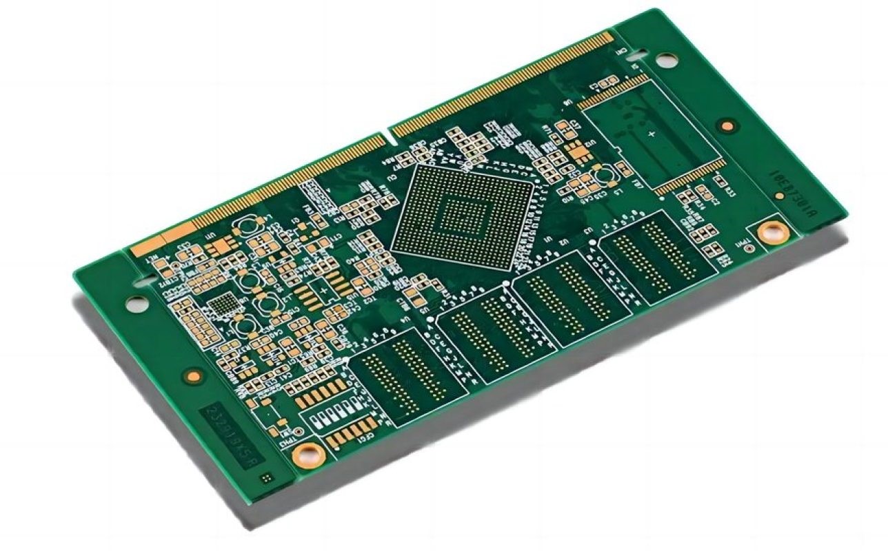
HDI PCB manufacturers in UK capability review for a complex project

How to Choose an HDI PCB Manufacturer in UK?

Choose an HDI PCB manufacturer in UK by matching the proposed factory, process controls and evidence package to your board. A UK address may represent a fabrication site, sales office, managed supply service or assembly provider, so the quotation should name where the bare board will be produced and which operations are subcontracted.

  • Match the buildup: submit the layer stack and microvia start/stop layers so the supplier cannot silently simplify the routing concept.
  • Confirm materials: identify the laminate family, electrical properties and acceptable substitutions because changes can alter impedance and pressing behavior.
  • Check prototype and production routes: ask whether both use the same site, materials and critical processes; define approval for any transfer.
  • Agree on evidence: specify electrical test, microsection, impedance verification, inspection reports and lot records before comparing prices.
  • Evaluate assembly ownership: for BGA, CSP or via-in-pad designs, determine how bare-board findings return to the assembly team.
  • Judge communication by output: a useful supplier returns a marked-up stackup, DFM questions, deviations and an evidence plan—not only a quick reply.

What Capabilities Should HDI PCB Manufacturers in UK Provide?

Look for capabilities that correspond directly to routing, component, signal-integrity and reliability requirements. Minimums depend on layer count, copper weight, material, panel size and volume.

HDI process capability Published UK capability example
Maximum layer count Up to 32 layers
Laser microvia diameter Down to 75 µm
Mechanical drill diameter Down to 0.105 mm
Fine track and gap Down to 50 µm
Microvia aspect ratio Up to 1:1
Sequential lamination Up to 6 lamination cycles
Supported via structures Blind, buried, stacked and staggered microvias
Via filling Copper-filled and resin-filled vias
Controlled impedance ±10% standard; ±5% advanced capability
Electrical test 100% electrical test

The numerical examples above are currently published by Exception PCB for its UK HDI production environment; Rush PCB UK separately publishes up to 20+ layers, 0.1 mm microvias and 50/50 µm trace/space. These are screening references, not universal limits for all HDI PCB manufacturers in UK. Require the shortlisted factory to return values tied to your material, copper, panel and volume.

How Can You Verify a Reliable HDI PCB Manufacturer in UK?

A reliable manufacturer connects each important claim to a site-specific process, review record and acceptance method. Certificates may support qualification, but they do not prove that a particular microvia stack has been assessed.

  • Build-specific DFM: require comments tied to actual layer pairs, microvia spans, copper, materials and tolerances. A generic “approved” response does not show that the construction was reviewed.
  • Named production site: record the physical factory and which processes it performs. If laser drilling, filling or testing is subcontracted, require the responsible site and control method.
  • Material traceability: record manufacturer, grade and lot identity, and require approval before substitution. This protects impedance and lamination behavior from unreviewed changes.
  • Microvia evidence: agree on microsection locations, plating and fill criteria, sampling frequency and the report supplied with the order.
  • Electrical and impedance testing: define the source netlist, test coverage, coupon design, target tolerance and report format rather than accepting “tested” as a complete answer.
  • Registration control: ask how sequential-lamination registration is monitored and what evidence demonstrates that capture pads and interlayer alignment meet the drawing.
  • Prototype-to-production consistency: confirm whether the same stackup, material, factory and critical process route will be used after prototype approval.
  • Change and nonconformance control: define which changes need written approval and who owns containment, root-cause analysis and corrective action after fabrication or assembly.

Request report samples before ordering. This proves the evidence is part of the operating process rather than a document requested after the boards are finished.
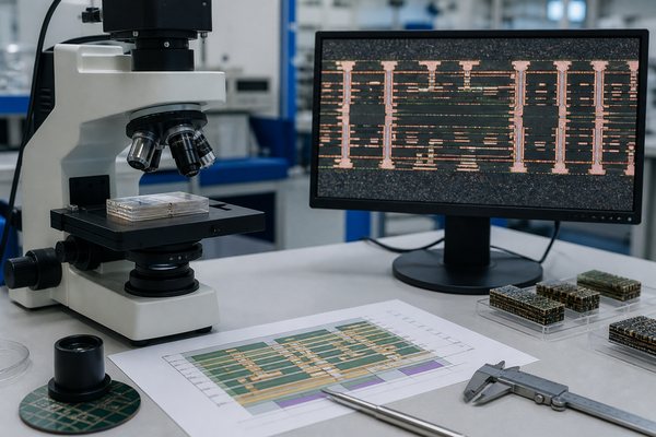
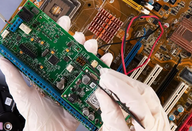
Reliability review of an HDI PCB microsection and plated microvias

Why Choose EBest as an Alternative to HDI PCB Manufacturers in UK?

When UK production is not a contractual requirement, EBest Circuit offers a China-based route that connects HDI fabrication, engineering review and PCB assembly. EBest is not presented as a UK manufacturer; it is an alternative for UK projects needing coordinated overseas manufacturing.

  • Build-specific review: stackup, microvia map, via-in-pad, materials and impedance are reviewed against the intended construction.
  • DFM before production: Gerber or ODB++, drill data and notes are checked for ambiguous transitions, conflicts and avoidable complexity.
  • Fabrication and assembly coordination: board production, sourcing, SMT, inspection and test can share one project workflow.
  • Prototype-to-volume control: approved data, revisions and deviations can be retained for later builds.
  • Project-defined evidence: electrical test, AOI, microsection, impedance and assembly inspection are scoped to the design.
  • Pre-quotation support: unresolved manufacturing and assembly questions are identified before commercial comparison.

Send Gerber or ODB++, stackup, drill files and project requirements to sales@bestpcbs.com for a free DFM review and quotation.

How Should You Compare Quotes From HDI PCB Manufacturers in UK?

Compare quotations only after every HDI PCB manufacturer in UK has priced the same construction, production route and acceptance evidence. Use the following checks:

  • Freeze the technical baseline: use one released stackup, via map, material requirement, copper weight, surface finish and impedance table. Otherwise, a lower quote may represent a simpler board.
  • Separate setup from unit price: identify tooling, engineering, coupons and one-time test charges so repeat-order cost is visible.
  • Confirm the buildup assumption: require the quoted lamination cycles and stacked/staggered microvia treatment in writing because they are major cost drivers.
  • Check included evidence: state whether electrical test, impedance reports, microsections, first-article records and certificates are included or charged separately.
  • Identify the production site: compare UK-built, UK-managed and overseas manufacture honestly; include freight, import handling and any transfer risk.
  • Normalize quantity and delivery: request the same prototype, pilot and repeat-order quantities with the same delivery point and required date.
  • List every deviation: a quote that substitutes material or omits a process is not comparable until the difference is reviewed and accepted.

Which Design Choices Increase Quotes From HDI PCB Manufacturers in UK?

Design choices increase cost when they add process cycles, reduce yield or require tighter verification. DFM can reduce those costs without weakening function.

  • Extra buildup cycles: each adds pressing, drilling, imaging and registration work.
  • Stacked microvias: use them for necessary vertical transitions; staggered structures may be simpler when routing permits.
  • Filled and capped vias: restrict them to locations that require pad escape, thermal or assembly performance.
  • Fine features: review local bottlenecks instead of applying an extreme rule across the board.
  • Specialty materials: specify performance needs and permitted alternatives to avoid unnecessary sourcing constraints.
  • Inspection: connect each extra record or test to a real risk and acceptance decision.

What Lead Time Should You Expect From an HDI PCB Manufacturer in UK?

Published UK supplier examples place HDI prototypes from about 5 working days, while more complex HDI/BBV builds are commonly presented around 7–10 working days. Some suppliers advertise 1–5-day expedited options, but those are conditional services rather than a dependable default for every stackup.

Planning case Indicative published range What can extend it
Simple, materials-available HDI prototype From about 5 working days Open DFM questions, special material, via filling or added reports
More complex HDI or blind/buried-via build About 7–10 working days as a planning reference Multiple lamination cycles, stacked vias, tight registration or non-stock laminate
Expedited service Some UK suppliers advertise 1–5 working days Available only after design, material, capacity and inspection review
HDI plus assembly Bare-board lead time plus component and PCBA schedule Long-lead components, stencil, programming, X-ray or functional testing

The ranges are based on current supplier-published examples: Pure PCB lists HDI prototypes from five working days and an HDI/BBV range of 7–10 days, while Rush PCB UK advertises conditional 1–5-day quick-turn options. Treat them as RFQ planning references, not EBest promises or universal UK lead times. Ask the selected manufacturer to return a milestone schedule covering DFM approval, material release, lamination, drilling/filling, inspection, assembly and shipping.

How Should an HDI PCB Manufacturer in UK Select Materials?

An HDI PCB manufacturer in UK should select a material system from the electrical requirement, thermal exposure, lamination sequence, thickness target and supply risk—not from Tg alone.

  • For standard digital and industrial HDI: confirm that the chosen high-Tg FR-4 supports the required press cycles and finished thickness without uncontrolled material substitution.
  • For high-speed or RF nets: provide target Dk/Df assumptions, frequency and impedance geometry so the fabricator can model the actual construction.
  • For repeated reflow or higher thermal demand: review decomposition behavior, z-axis expansion and moisture control together with the assembly profile.
  • For thin dielectrics and microvias: verify that prepreg and core availability supports the required microvia depth, resin flow and copper distribution.
  • For procurement continuity: name the preferred grade and approved equivalent criteria; require notification before any change that affects impedance or lamination.

The RFQ should record manufacturer, grade, dielectric construction, copper type and weight, required electrical data, approved alternatives and substitution authority. The reviewed production stackup should be returned before release.

How Should an HDI PCB Manufacturer in UK Control Via-in-Pad?

An HDI PCB manufacturer in UK should control via-in-pad as a complete fill, cap and surface-planarity process. The buyer should verify:

  • Via geometry: define drill diameter, depth, aspect ratio and connected layers so the fill process is evaluated against the real structure.
  • Fill and cap: state whether conductive or non-conductive fill is required, the copper-cap expectation and any void acceptance criterion.
  • Planarity: specify the finished BGA/CSP pad requirement and inspection method because uneven pads can change paste volume and joint formation.
  • Surface finish: review finish selection and thickness after planarization; the final pad, not the unprocessed via, must meet assembly needs.
  • Fabrication-to-PCBA feedback: align stencil, reflow and X-ray inspection with pad acceptance so solder defects can be separated from bare-board defects.

Put these requirements in the fabrication drawing and via map. Do not rely on a note that says only “VIPPO” or “via-in-pad,” because it does not define the acceptance result.

How Should an HDI PCB Manufacturer in UK Plan Sequential Lamination?

An HDI PCB manufacturer in UK should translate the via map into a documented sequence of core preparation, lamination, laser drilling, filling and inspection.

  • Map every microvia span: show which vias are formed after each press cycle and where stacked interfaces occur.
  • Confirm the minimum necessary cycles: extra buildup stages increase alignment work, cost and lead time; remove a cycle when routing permits a simpler transition.
  • Control materials through repeated pressing: verify dielectric thickness, resin behavior and copper balance for the complete thermal history.
  • Protect registration: review capture pads, material movement allowances and the evidence used to verify interlayer alignment.
  • Define stage-specific inspection: identify which structures require microsection or other checks before later layers make them inaccessible.
  • Freeze the production stackup: require approval before changing layer sequence, material, site or via structure after prototype acceptance.
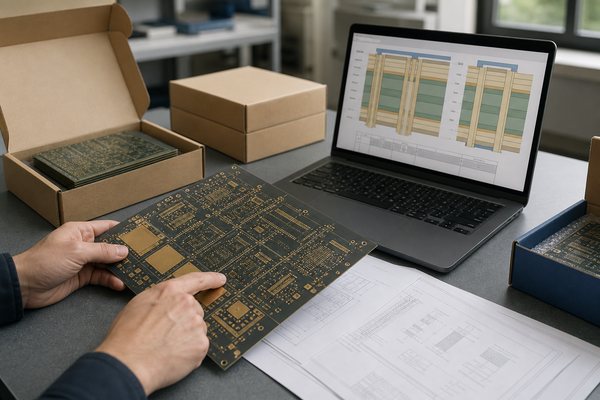
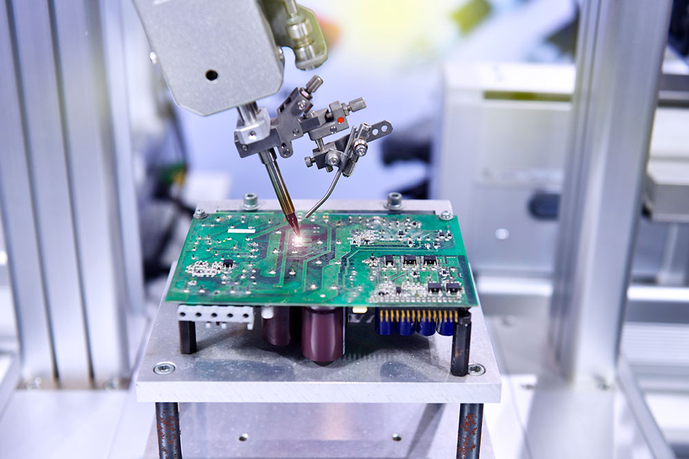
HDI PCB fabrication and assembly requirements reviewed in one workflow

What Files Should You Send to an HDI PCB Manufacturer in UK?

A useful quote needs enough released data to identify the actual process route. Send the same package to each supplier.

  • Gerber or ODB++: release the copper, mask, legend and profile geometry from one controlled revision.
  • NC drill and microvia map: distinguish mechanical, buried, blind and laser-drilled holes and show every start/stop layer.
  • Production stackup: define the buildup, dielectric thicknesses, copper weights, material grades and finished thickness.
  • Fabrication drawing: state finished-hole rules, via fill/cap, surface finish, tolerances and special acceptance notes.
  • Impedance table: identify nets, layers, target, tolerance, reference planes and required reporting.
  • Quantity schedule: separate prototype, pilot and repeat volumes so tooling, panelization and unit pricing can be compared.
  • PCBA data when required: include BOM, pick-and-place, assembly drawing, approved substitutions and component-sourcing scope.
  • Inspection and test requirements: define electrical test, microsection, impedance, X-ray, programming and functional-test deliverables as applicable.
  • Commercial inputs: provide delivery destination, required date, Incoterm request and any country-of-manufacture restriction.

Also state prototype and repeat quantities, destination, origin constraints and required records. Ask for a reviewed stackup, deviations, proposed site and included inspection scope.

Submit the complete package with the RFQ and request an HDI DFM review covering both fabrication and assembly requirements.

How Should HDI PCB Manufacturers in UK Prevent Common Defects?

Prevent the main HDI defects by controlling the design input, process window and inspection point for each risk:

  • Microvia interconnect failure: keep the via diameter, depth and aspect ratio inside the approved process window; control laser drilling, interface preparation and plating; verify critical structures by electrical test and targeted microsection.
  • Incomplete via fill: match copper or resin fill to the via geometry, define acceptable voiding and inspect the filled structure before later processing hides it.
  • Poor via-in-pad planarity: specify fill, cap-plating and finished-pad requirements; inspect the surface before assembly to prevent solder wicking and inconsistent joints.
  • Layer misregistration: provide adequate capture pads, account for material movement and check alignment after each relevant lamination stage rather than only at final inspection.
  • Delamination: use a compatible material system, control moisture and contamination, and validate the press and thermal history for repeated lamination and reflow.
  • Impedance deviation: freeze dielectric thickness, copper geometry and material data in the production stackup; measure agreed coupons against the stated tolerance.
  • Open or short circuits: run 100% electrical testing against the correct released netlist and keep repair or concession records tied to the lot.
  • Prototype-to-volume drift: prevent unapproved changes to the factory, material, stackup, via treatment and inspection plan after the prototype is accepted.

FAQs About HDI PCB Manufacturers in UK

Q1: Are HDI PCBs always more expensive than standard multilayer PCBs?

A1: They usually involve additional processes, but the difference depends on buildup, microvias, materials, testing and quantity.

Q2: What is the minimum layer count for an HDI PCB?

A2: Layer count alone does not define HDI; high-density interconnection methods do.

Q3: Are stacked microvias better than staggered microvias?

A3: Neither is universally better. Select the structure from routing need and manufacturing risk.

Q4: Can HDI PCBs use controlled impedance?

A4: Yes. Provide target, tolerance, geometry and material assumptions and agree on coupon reporting.

Q5: Which surface finish suits fine-pitch HDI assembly?

A5: Choose it from pad geometry, assembly, storage and reliability needs, then review planarity with the assembler.

Q6: Do all microvias need to be filled?

A6: No. Filling depends on structure and use; via-in-pad and some stacked configurations need a defined fill and cap.

Q7: Should prototype and volume boards use the same stackup?

A7: The prototype should represent production where possible; later changes may require review or requalification.

Q8: Is DFM review necessary before production?

A8: Yes. It can find conflicting via structures, unsupported rules and incomplete acceptance criteria.

Q9: Can HDI boards use fine-pitch BGA and CSP packages?

A9: Yes, when pads, via treatment, finish, stencil, reflow and inspection are coordinated.

Q10: How should UK and overseas suppliers be compared?

A10: Use identical files, quantities, evidence, assembly scope, destination and change controls, then compare total responsibility and risk.

Conclusion

The right supplier turns a released HDI design into a controlled, inspectable and repeatable manufacturing plan. Confirm the build site, match capabilities to the stackup, require project-specific evidence and compare quotes on identical assumptions. Whether the route is UK in-house, UK-managed or overseas, technical ownership must remain clear from DFM through repeat production.

For an EBest quotation, send Gerber or ODB++, drill files, stackup, microvia map, fabrication drawing, impedance requirements, quantities, BOM, assembly data and test scope to sales@bestpcbs.com.

You may also like

HDI PCB Assembly Manufacturing & Manufacturer, Over 19 Years
Tuesday, November 4th, 2025

How to assemble HDI PCB? Let’s discover benefits, applications, manufacturing process, manufacturer recommendations for HDI PCB assembly.

Are you worried about these problems?

  • Struggling with high-density routing complexity and time-consuming design revisions?
  • Facing yield instability and cost control issues under miniaturization demands?
  • Tight deadlines and urgent orders causing production scheduling headaches?

As a HDI PCB assembly manufacturer, EBest Circuit (Best Technology) can provide you solutions:

  • Dedicated HDI design team with DFM-driven early engagement to slash trial cycles by 30%+;
  • Smart layer stacking optimization + laser microvia tech ensuring micro-spacing reliability, stabilizing yield at 98%+ while cutting costs by 15%;
  • Agile capacity pool + real-time scheduling system for 7-day rush order response and 24/7 lead time tracking.

Welcome to contact us if you have any issues with HDI PCB assembly: sales@bestpcbs.com.
What Is HDI PCB Assembly?

HDI PCB Assembly refers to the process of soldering and interconnecting electronic components on highly compact and complex High Density Interconnect circuit boards using advanced manufacturing techniques, such boards include the use of microvias (e.g., blind or buried vias formed via laser drilling), finer line widths/spacings, increased routing layers, and tightly stacked interlayer technologies, enabling significantly higher routing density and electrical connection complexity within smaller areas compared to traditional PCBs.

This assembly process demands ultra-high-precision placement equipment (such as for miniature BGA or CSP chips), precise soldering techniques (e.g., laser soldering or specialized reflow processes), and rigorous inspection methods to ensure reliable electrical connections and functionality of all components and microvia interconnections in such miniaturized spaces.

What Is HDI PCB Assembly?

Why Choose HDI PCB Assembly?

Benefits of HDI PCB Assembly:

  • Maximizing Space Utilization Efficiency: HDI technology employs microvias, blind vias, and buried vias to drastically reduce wiring area, enabling complex circuit layouts within limited space. This supports compact structural designs for volume-sensitive products like smartphones and wearables.
  • Enhancing Electrical Performance and Signal Integrity: Shortened signal transmission paths minimize impedance and signal attenuation while reducing electromagnetic interference (EMI). This ensures stable data transmission quality in high-frequency applications such as 5G communication devices.
  • Increasing Design Flexibility and Integration: Supports high-density arrangement of components on double-layer or multi-layer boards, allowing seamless integration of complex functional modules (e.g., processors, sensors). Any-Layer Interconnect (ELIC) schemes break traditional PCB wiring constraints.
  • Improving Reliability and Durability: Microvia technology reduces mechanical stress concentration points, enhances thermal cycling performance, and extends product lifespan. Stringent lamination and copper plating standards lower connection failure risks, meeting high-reliability demands in automotive electronics and medical devices.
  • Accelerating Product Development Cycles: HDI design facilitates rapid prototype verification, streamlines debugging processes, and shortens the transition from design to mass production. Strong compatibility with simulation tools optimizes pre-development schemes and reduces trial-and-error costs.
  • Reducing Long-Term Comprehensive Costs: Although initial costs are higher, HDI reduces material layers, optimizes assembly processes, and lowers material and labor inputs. Higher yield rates and product reliability minimize post-sales maintenance expenses, boosting overall economic efficiency.
  • Driving Technological Iteration and Innovation: Serves as a carrier for advanced packaging technologies (e.g., wafer-level packaging), supporting R&D in cutting-edge fields like AI chips and IoT devices. Compatible with new materials (e.g., high-frequency substrates) to adapt to future electronic technology evolution.
  • Environmental and Sustainability Benefits: Precise material usage minimizes waste and complies with environmental standards like RoHS. Energy-efficient designs reduce power consumption in end products, aligning with green manufacturing trends.
Why Choose HDI PCB Assembly?

When to Use HDI PCB Board Assembly?

Applications of HDI PCB Board Assembly:

  • Smartphone motherboards
  • Wearable devices (smartwatches, wireless earphones)
  • Automotive ADAS controllers
  • In-vehicle entertainment systems and dashboards
  • Portable medical devices (ultrasound diagnostic instruments, blood glucose monitors)
  • Implantable medical devices (pacemakers, nerve stimulators)
  • Satellite communication modules
  • Military radar and navigation systems
  • Server and data center motherboards
  • Edge computing devices
  • Industrial PLCs
  • Smart home controllers

HDI PCB Assembly Manufacturing Processes

1. Incoming Quality Control (IQC)

  • Visual Inspection: Use high-magnification microscopes or automated optical inspection systems to detect defects on HDI PCB bare boards (e.g., scratches, copper peeling, solder mask delamination) and electronic components (e.g., oxidized/bent leads).
  • Specification Verification: Utilize XRF spectrometers to validate PCB substrate specifications (copper thickness, layer count, dielectric constant); employ calipers/micrometers to measure component dimensional accuracy.
  • Soldability Testing: Conduct wetting balance tests to evaluate solder paste adhesion to pads/component leads; perform thermal shock tests for surface finishes like OSP/ENIG.
  • Standards Compliance: Cross-reference IPC-A-610 for pad design/solder mask tolerances; JEDEC standards for chip package dimensions; ASTM D2794 for adhesion testing.
  • Batch Traceability: Implement barcode/QR code systems to track material batches, suppliers, and storage dates for full lifecycle traceability.

2. Solder Paste Printing

  • Stencil Design: For fine-pitch components (e.g., 01005), use electroformed nickel stencils with ±5μm aperture accuracy; implement stepped stencils for BGA/CSP areas to control solder volume.
  • Machine Parameters: Set squeegee pressure (2-5N/cm?), print speed (50-150mm/s), and snap-off speed (0.1-0.3mm/s); employ SPI (Solder Paste Inspection) for real-time 3D measurement of print thickness (0.08-0.15mm) and alignment (±15μm).
  • Quality Control: Utilize 3D SPI for defect detection (bridging, insufficient solder, misalignment); perform localized magnified inspection for microvia regions; document parameters in a process database.

3. Surface Mount Technology (SMT) Placement

  • Equipment Precision: High-precision pick-and-place machines achieve ±15μm accuracy for 01005 (0.4mm×0.2mm) components; vision systems enable precise BGA/CSP alignment.
  • Process Optimization: Conduct DOE (Design of Experiments) to determine optimal placement pressure/nozzle height; implement segmented placement strategies (large components first, then small ones).
  • Special Handling: Use vacuum nozzles/non-contact grippers for QFN/LGA devices; configure dedicated placement heads for temperature-sensitive components with controlled speed.

4. Reflow Soldering

  • Temperature Profile Control: Utilize 10-zone reflow ovens with zones for preheat (150-180°C), soak (180-200°C), peak (217-227°C for lead-free alloys), and cooling (3-5°C/s); monitor via thermocouples.
  • Material-Specific Adjustments: Raise peak temperatures to 245-255°C for SAC305 solder; implement nitrogen inerting for high-speed/high-frequency substrates (e.g., Rogers 4350B).
  • Defect Prevention: Perform thermal simulation to predict stress distribution; conduct board-level reliability testing (-55°C~125°C thermal cycling) for BGA packages; monitor oven uniformity via infrared thermography.

5. Automated Optical Inspection (AOI)

  • Detection Algorithms: Deploy deep learning for 01005 component defects (misalignment, tombstoning); multi-angle lighting for bridging/insufficient solder detection; tilted-view imaging for QFN bottom terminations.
  • Defect Classification: Build AI-powered defect libraries for automatic categorization (wrong parts, missing components, polarity reversal); implement false-positive filtering.
  • Data Traceability: Generate inspection reports with images/defect locations; integrate with MES for real-time production data synchronization.

6. Through-Hole Technology (THT) Insertion

  • Insertion Strategy: Use selective insertion machines for high-density areas; equip manual stations with ESD workbenches/magnifiers.
  • Process Control: Monitor insertion depth via force sensors; pre-form THT leads (e.g., 90° bending) to suit HDI density constraints.
  • Soldering Protection: Shield SMD areas with fixtures; apply localized cooling for temperature-sensitive components; optimize wave solder parameters (time/temperature) to minimize thermal impact.

7. Wave & Selective Soldering

  • Wave Parameters: Set wave temperature (250-260°C), height (8-12mm), and conveyor speed (1.0-1.5m/min); employ nitrogen inerting to reduce oxidation.
  • Selective Soldering: Use robotic solder nozzles for point-to-point welding; laser alignment ensures precision; dual-nozzle systems for high-power device leads.
  • Defect Detection: Perform X-ray inspection for hidden joints; conduct pull testing for mechanical strength; use dye penetrant tests for micro-cracks.

8. Hand Soldering & Rework

  • Tool Configuration: Equip 200-300W soldering stations with microscopes/vacuum desoldering tools; use lead-free solder (Sn96.5Ag3Cu0.5) with temperature control.
  • Operational Standards: Standardize rework procedures (heat first, then add solder); employ BGA rework stations for precision temperature control; apply localized cooling for sensitive parts.
  • Quality Validation: Microscopic inspection for wetting quality; electrical testing for functional recovery; document rework processes for traceability.

9. Cleaning & Coating

  • Cleaning Process: Ultrasonic cleaning with aqueous detergents for flux removal; solvent cleaning (e.g., n-hexane) for high-reliability applications with exhaust treatment.
  • Coating Techniques: Automated conformal coating with acrylic/silicone/polyurethane; measure film thickness (25-75μm) via thickness gauges; localized reinforcement for critical areas.
  • Potting Process: Encapsulate with two-part epoxy resins; vacuum degassing for bubble removal; thermal curing with insulation resistance testing.

10. Testing & Burn-In

  • Electrical Testing: ICT uses bed-of-nails fixtures for component-level testing; flying probe testers contact high-density points without dedicated fixtures; boundary scan (JTAG) for chip-level tests.
  • Functional Verification: FCT simulates operational conditions (power fluctuations, signal interference) for system validation; eye diagram tests for high-speed digital circuits; S-parameter measurements for RF circuits.
  • Reliability Testing: Conduct 85°C/85%RH tests, -55°C~125°C thermal cycling, and vibration testing (sine/random); perform shear testing for critical solder joints.

11. Packaging & Logistics

  • Packaging Standards: Multi-layer packaging with ESD shielding bags, foam, and desiccants; vacuum packaging for precision components; reinforced crates for large PCBAs.
  • Logistics Tracking: Implement barcode/RFID systems for product traceability; monitor temperature/humidity during transit; secure high-value shipments with insurance.
  • Documentation: Provide complete process files (BOMs, parameter sheets), test reports, and reliability data; integrate with EDMS (Electronic Document Management System).
HDI PCB Assembly Manufacturing Processes

Why Choose EBest Circuit (Best Technology) as HDI PCB Assembly Manufacturer?

Reasons why choose us as HDI PCB assembly manufacturer:

  • 19 Years of Dedicated HDI Expertise: With 19 years of focused experience in HDI PCB assembly, we cover full-spectrum HDI technologies from 2-stage to 8-stage any-layer solutions. Having completed over 5,000 high-complexity projects, we deliver proven process expertise and problem-solving capabilities as your reliable long-term technical partner.
  • ISO-Certified Quality Control System: Adhering to IPC-A-610E/620A standards and our proprietary “dual-inspection, triple-review” process, we implement 360° full-chain traceability from component incoming to final shipment. Defect rates are controlled below 50PPM, with products certified to ISO9001/14001 and RoHS standards, ensuring zero-defect precision for every board.
  • Competitive Price: Through scaled production, lean supply chain management, and process optimization, we offer prices 15%-20% below market averages while maintaining cost advantages for premium materials (e.g., high-frequency substrates) and specialized processes (e.g., blind/buried vias, microvia filling), maximizing your cost-performance value.
  • One-Stop Solutions: From PCB design optimization and BOM sourcing to SMT assembly, testing, and logistics, we provide end-to-end integrated services that reduce supplier coordination efforts, shorten project timelines by over 30%, and deliver true turnkey convenience.
  • Fast Delivery for Market Leadership: Leveraging intelligent production scheduling and flexible capacity allocation, standard HDI projects achieve 7-day prototyping and 15-day volume production. Urgent orders are supported with 48-hour expedited responses, enabling faster market entry and competitive advantage.
  • Precision Equipment for Micron-Level Accuracy: Equipped with imported systems like JUKI high-speed placement machines, combined with AOI and X-ray inspection, we achieve ±0.05mm microvia processing accuracy and 01005 component placement capability to meet the most demanding design specifications.
  • Custom R&D Support for Technical Challenges: Our 30+ senior engineers provide full-chain technical support, including DFM analysis, signal integrity simulation, and development of specialized processes (e.g., rigid-flex boards, embedded components), helping you overcome technical barriers and drive innovation.
  • Sustainable Manufacturing for Global Compliance: We employ lead-free processes, water-based cleaning agents, and recyclable packaging while complying with EU REACH, halogen-free, and other environmental regulations. Carbon footprint tracking optimizes energy use, ensuring seamless compliance with global green standards.

Our Quality Inspection for HDI PCB Assembly

Raw Material Inspection

  • Substrate Testing: Utilize TMA thermomechanical analyzer and dielectric constant tester to validate dielectric constant (Dk deviation ≤ ±0.05, frequency range 1MHz-10GHz), CTE (Coefficient of Thermal Expansion ≤12ppm/℃, -50℃ to 250℃), and water absorption rate (≤0.1%).
  • Copper Foil Inspection: Employ universal material testing machine to ensure thickness deviation ≤ ±5% (precision 0.1μm), tensile strength ≥250MPa (electrodeposited copper) / ≥300MPa (rolled copper), and peel strength ≥0.7kgf/cm.
  • Solder Mask Material Inspection: Apply insulation resistance tester and solderability testing device to confirm insulation resistance ≥10¹²Ω (500V DC), solderability (no blistering/delamination after 10-second dip in 260℃ solder), and chemical resistance (no appearance change after 24-hour immersion in alcohol/acetone).

Process Inspection

  • Laser Drilling Inspection: Use X-ray fluorescence thickness gauge and optical microscope to verify hole diameter tolerance ≤ ±3% (hole size ≤0.15mm), copper wall thickness deviation ≤1μm, and ensure hole position tangent to target pad without pad damage.
  • Plating Layer Inspection: Validate copper/nickel/gold layer thickness compliance with design specifications (precision 0.01μm) and fixed plating current density at 1.5A/dm² (verified via DOE) using film thickness tester.
  • Laminate Quality Inspection: Employ metallographic microscope and thermal stress tester to confirm layered dielectric thickness ≥40μm after lamination (minimum thickness ≥30μm) and absence of bubbles/delamination.

Inline Detection

  • AOI Optical Inspection: Deploy high-precision AOI equipment to detect line width deviation ≤ ±10% (pixel accuracy 0.001mm), identify defects like shorts/opens/metal residues, maintain false call rate ≤0.1%, and achieve detection speed ≥1m/min.
  • X-ray Inspection: Utilize X-ray detection system to check blind/buried via alignment accuracy ≤0.005mm, detect copper voids/layer misalignment, and enable full-board non-destructive testing.
  • Electrical Testing: Use flying probe tester and hipot tester to verify circuit continuity, insulation resistance ≥10MΩ (40V), and withstand voltage ≥1000VDC without breakdown.

Final Product Reliability Inspection

  • Environmental Adaptability Testing: Conduct temperature cycling (-40℃ to 125℃, 1000 cycles, resistance change ≤10%), damp heat aging (85℃/85% RH, 1000 hours, insulation resistance ≥10¹⁰Ω), and vibration testing (10-2000Hz, 20g acceleration, no structural damage) via environmental chambers and shakers.
  • Solder Joint Reliability Testing: Perform thermal shock (-55℃ to 125℃, 1000 cycles, solder joint failure probability ≤1%) and dynamic bending (flexible PCB, bending radius 5mm, 10000 cycles no fracture) using thermal shock chambers and bending testers.
  • Signal Integrity Testing: Measure signal loss, delay, and noise using high-speed oscilloscopes and network analyzers to ensure transmission stability meets design requirements.
Our Quality Inspection for HDI PCB Assembly

Our HDI PCB Assembly Capabilities

ItemCapabilities
Placer Speed13,200,000 chips/day
Bare Board Size0.2 x 0.2 inches – 20 x 20 inches/ 22*47.5 inches
Minimum SMD Component01005
Minimum BGA Pitch0.25mm
Maximum Components50*150mm
Assembly TypeSMT, THT, Mixed assembly
Component PackageReels, Cut Tape, Tube, Tray, Loose Parts
Lead Time1 – 5 days

How to Get a Quote For HDI PCB Assembly Service?

All Documents for HDI PCB Assembly Service Quotation:

  • Gerber Design Files: Complete circuit layer designs (including copper layers, solder mask, silkscreen, etc.) to ensure precise circuit replication.
  • Bill of Materials (BOM): Detailed list of components with model numbers, specifications, quantities, and supplier information for material procurement and cost calculation.
  • Drill Files: Clear specifications of hole positions, diameters, and types (e.g., blind/buried vias) to meet HDI high-density routing requirements.
  • Assembly Drawing/Coordinate Files: Precise coordinates of components on the PCB to guide SMT placement and soldering, avoiding misalignment.
  • Process Parameters: Surface finish (e.g., ENIG, HASL), solder mask color, substrate material (FR4/high-frequency), board thickness, layer count, and special processes (e.g., blind/buried vias, microvia filling).
  • Test Verification Files: Test point diagrams and functional test plans to validate circuit performance.
  • Quantity & Lead Time Requirements: Production batch size (prototype/small batch/mass production), delivery time, and urgency level affecting production scheduling and costs.
  • Contact & Contract Information: Company name, contact person, contact details, and agreement clauses for communication and legal compliance.

Welcome to contact us if you have any request for HDI PCB assembly: sales@bestpcbs.com.

You may also like