PCB board stiffeners are supports that reinforce selected areas of a printed circuit board without turning every flexible section into a rigid board. In flexible circuits, they commonly support connectors, component mounting areas and contact fingers. In assembly equipment, the same term can describe removable supports that hold a board during processing. Choosing the right construction starts with separating these two jobs, then checking material, bonded thickness and the forces at each support edge.
What Is Stiffener in PCB?
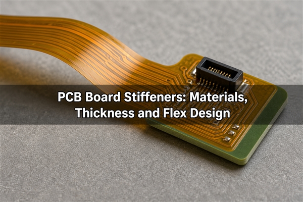
A PCB stiffener is an added mechanical layer, not an extra signal-routing layer. An FR4 backing piece can keep a connector area flat, while a polyimide backing film can bring a flexible contact tail to the thickness required by its socket. The electrical conductors remain in the circuit, rather than in the ordinary stiffener.
A circuit board stiffener is therefore different from increasing copper weight or adding another conductive layer. The components of PCB board assemblies still need electrically sound pads, traces and joints; reinforcement only changes their mechanical support. FPC stiffener and flex circuit stiffener are names used for this local reinforcement on flexible printed circuits.
How Can You Stiffen a PCB?
For a flexible circuit, bond a suitable backing to the area that must resist handling or connector loads. For a rigid assembly, consider its supports, fasteners, rail spacing or assembly fixture before changing the laminate. The useful question is where the force enters the board and where that force can safely leave it.
- Connector area: resist insertion, extraction and cable-pull loads without bending nearby solder joints.
- Component island: provide stable support beneath a populated flex area while leaving the intended bend zone flexible.
- Contact tail: control mating thickness and handling stiffness without covering exposed contacts.
- Assembly panel: reduce sag or handling movement with a carrier or removable panel stiffener.
A custom board stiffener should follow a defined load path. A larger backing is not automatically better: it can move bending into a shorter, more highly strained section of flex.
Which PCB Stiffener Material Should You Use?
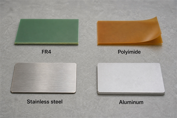
Compare the mechanical job before comparing PCB board material types. FR4, polyimide and metal backings are not interchangeable merely because their outlines match. FPC stiffener material selection must also account for adhesive, insulation, temperature exposure and available height.
| Material | Typical role | Important constraint |
|---|---|---|
| FR4 stiffener | Local support beneath connectors or component areas | Leaves a relatively abrupt rigid-to-flex transition; hole access and edge placement matter. |
| Polyimide stiffener | Thin backing for contact tails and local thickness adjustment | Provides less rigidity than a substantial FR4 backing; the complete bonded stack determines fit. |
| Stainless steel | Compact, high-rigidity reinforcement where the design justifies metal | Conductive edges need clearance or insulation; burrs and bonding surfaces require control. |
| Aluminum | Mechanical backing with a possible thermal role | Heat spreading depends on the actual interface and heat path, not the metal name alone. |
For a steel board stiffener or copper board stiffeners, include the conductive backing in clearance and grounding reviews. A metal support must not accidentally bridge exposed pads or test points.
How Do You Choose PCB Stiffener Thickness?
PCB stiffener thickness must be selected together with the circuit and bond line. A finished contact tail is thicker than the backing alone. For a component island, the constraint may instead be allowable deflection, enclosure clearance or the height of a nearby mounting boss.
Finished supported thickness = flex-circuit thickness + cured adhesive thickness + stiffener thickness. Use the thickness of the actual local circuit region, including the layers present there. Do not add coverlay twice or assume that the contact-finger region matches the covered region.
| Illustrative stack element | Nominal thickness |
|---|---|
| Local flex circuit | 0.100 mm |
| Cured adhesive | 0.025 mm |
| Selected backing | 0.175 mm |
| Finished supported section | 0.300 mm |
This is an arithmetic example, not a stock material recommendation. If the respective tolerances were ±0.010, ±0.005 and ±0.015 mm, their worst-case sum would be ±0.030 mm. A nominal 0.300 mm result would then span 0.270-0.330 mm and would need to fit the connector’s permitted range.
PCB standard thicknesses for rigid boards do not establish the correct flex circuit stiffener thickness. The controlling requirement remains the selected connector drawing, not a generic PCB thickness value.
How Does a Flex PCB Stiffener Fit a ZIF Connector?
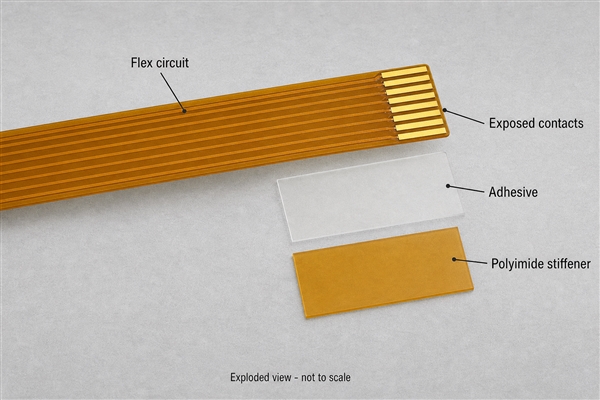
A ZIF connector needs the correct tail thickness, contact orientation, insertion length and outline. A flex PCB stiffener normally backs the non-contact side where the connector drawing requires it. It must not extend over the mating pads or obstruct the latch.
Check contact-side versus back-side orientation in a section view. Then verify the supported length, shoulder locations and available space after the latch closes. Too much thickness can obstruct insertion; too little can compromise retention or contact pressure. Neither condition should be corrected by forcing the latch.
A flex circuit with stiffener should be checked as a bonded assembly. Measure the finished tail at the specified location, then verify fit with the actual connector. Supplier examples of 0.20 mm or 0.30 mm tails are not permission to use those values for every socket.
Where Should Stiffeners End in Flex PCB Design?
Place the rigid boundary outside the intended active bend. In flex PCB design, an abrupt support edge can concentrate strain if the circuit repeatedly folds against it. Keep the supported island stable and provide enough free flex length for the required movement.
Stagger the coverlay termination and stiffener edge rather than aligning both boundaries at the same bend transition. Define the required overlap from the actual layer stack, fabrication tolerances and intended movement; one overlap dimension is not suitable for every construction.
Practical flex PCB guidelines must distinguish a one-time installation bend from continuous movement. A support near a fold does not make the fold dynamically rated. Confirm the bending direction, radius, number of cycles and distance to pads or vias with the fabricator. Our custom flex PCB design guide discusses the wider layout context.
How Are PCB Stiffeners Bonded?
Common approaches use pressure-sensitive adhesive or a heat-and-pressure bonding process. The adhesive grade, surface condition and process sequence determine whether the joint is suitable; the label PSA by itself does not establish reflow compatibility.
Before bonding, control contamination, backing flatness and registration. During bonding, follow the qualified pressure, temperature and time for the chosen system. Afterwards, inspect edge lift, trapped air, misalignment and adhesive squeeze-out. The PCB board process must also define whether reinforcement is installed before or after high-temperature assembly.
Review the complete thermal history, including multiple soldering passes and any later rework. Moisture conditioning and permitted cleaning chemistry should follow the actual material data. Do not substitute household tape or assume that a room-temperature peel test predicts hot-process performance.
What Must a Stiffener Drawing Define?
Show the support as a controlled mechanical feature, not an informal note. PCB board dimensions alone do not tell the fabricator which side receives the backing or whether a dimension describes the backing itself or the finished assembly.
- Identify backing material, nominal thickness and allowed tolerance.
- Define the bond system and finished supported thickness where it is functional.
- Dimension the outline, mounting holes and clearances from shared circuit datums.
- Identify the top or bottom side and the relation to exposed contacts and coverlay.
- Show bend keepouts, connector seating features and accessible inspection points.
An Altium flex stiffener design still needs an unambiguous fabrication view. A mechanical layer or 3D shape conveys geometry, but it does not automatically specify a bonding process or a qualified material. Check the exported files, not only the appearance in CAD.
In a plated through hole PCB, a conductive barrel belongs to the circuit. An ordinary backing clearance hole does not create an electrical interconnect. Size backing holes to allow for registration tolerance and solder access. Define the fabrication allowance on the drawing rather than assuming the backing and circuit holes should have identical diameters.
Stiffened Flex vs Rigid-Flex: What Is Different?
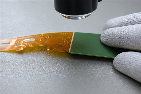
A printed circuit board stiffener provides support, whereas rigid-flex PCB construction combines electrically functional rigid and flexible sections. Bonding plain FR4 to a flex tail does not create plated connections to new rigid routing layers.
The distinction affects routing space, via structure, assembly access and validation. A support-only island can be sufficient for a connector. A design that needs dense routing or components on electrically integrated rigid sections may require a different architecture. Our rigid-flex PCB solutions integrate rigid and flexible circuit sections; they are not another name for a glued-on backing.
The term rigidflex describes the integrated construction; a stiffener board remains a mechanical support unless the design explicitly adds another electrical function.
Are PCB Edge Stiffeners the Same as Bonded Flex Backings?
No. PCB edge stiffeners used during assembly can be removable tooling. Titanium board stiffeners can clamp to PCB edges to support conveyor handling. Their function differs from a permanent reinforcement bonded beneath a flex connector.
A printed circuit board edge stiffener must leave components, conveyor features and required process access unobstructed. Board edge stiffeners and a carrier pallet also change how the board is supported during heating. Qualify that support arrangement with the actual assembly profile rather than treating the fixture as mechanically invisible.
For a thin panel stiffener, confirm whether it is retained in the product or removed after processing. We offer extra-thin PCB options at 0.15, 0.20, 0.25 and 0.30 mm. Those are board thicknesses, not standard stiffener thicknesses, and they make handling support an important design consideration. Panel support should be coordinated with PCB panelization and the assembly process.
What Can Go Wrong with a PCB Board Stiffener?
| Observed problem | Possible contributor | Useful verification |
|---|---|---|
| Tail will not seat | Excess total thickness, wrong side or misplaced shoulder | Measure finished geometry against the connector drawing. |
| Cracks near the backing edge | Bending concentrated at a support boundary | Inspect the transition and repeat the actual motion while monitoring continuity. |
| Backing lifts after heating | Bond preparation, material compatibility or thermal-process issue | Review process records and inspect conditioned samples after the intended thermal sequence. |
| Intermittent contact to metal backing | Insufficient insulation or clearance | Check electrical isolation under expected mechanical loading. |
| Solder access is blocked | Backing holes or outline do not match assembly needs | Review the assembled section and inspect real solder joints. |
A flat-looking board is not proof of reliability. Dimensional inspection, connector engagement, electrical continuity and application-specific mechanical testing address different failure modes. Record acceptance criteria before comparing samples so that a stronger backing does not hide a new transition failure.
How Does BestPCBs Support Reinforced Circuit Assemblies?
At EBest Circuit (Best Technology), we provide flexible circuits, rigid-flex boards and PCB assembly support. Our assembly capabilities include components as small as 01005 and BGA pitch down to 0.25 mm, subject to engineering evaluation. These capabilities do not replace reinforcement design: component placement, backing clearance and inspection access still need to work together on the actual assembly.
For a supported flex or thin-board assembly, the practical objective is a defined stack, an accessible assembly process and a verified mechanical interface. Discuss the circuit’s construction and intended motion with our engineering team at sales@bestpcbs.com.
Frequently Asked Questions
What does PCB stand for?
PCB stands for printed circuit board. A backing or stiffener supports the board but is not, by itself, a complete circuit.
Can you fix a bowed board with a stiffener?
Not reliably by simply forcing it flat. A support may limit deflection in a qualified design, but it does not repair cracked copper, damaged vias or delamination. Investigate the cause of bow and evaluate the board before applying force or heat.
Is a book binder flex PCB another type of stiffener?
No. Bookbinder construction uses separated flex layers with compensated lengths to accommodate different bend paths. It addresses multilayer bend geometry rather than adding local rigidity. Adding an extra backing layer does not reproduce this geometry.
Are through holes plated in a stiffener?
Ordinary mechanical backing holes need not be plated. They provide clearance or access, while electrical plated holes belong to the circuit design. The drawing must identify each hole’s purpose.
How do you choose material for stiffening PCB connector areas?
Start with the connector’s dimensions and forces. Then compare local rigidity, available height, electrical isolation and the bond system’s process compatibility. The best flex circuit stiffener material is the one that satisfies those constraints, not simply the thickest available backing.
Conclusion
Effective PCB board stiffeners support the areas that need stability while preserving the flex sections that must move. Select the material for its mechanical role, calculate the full bonded thickness, keep the transition out of the active bend, and verify the final assembly. Permanent flex reinforcement and temporary board-support tooling require different drawings and different checks.